
88MaxPower Semiconductor Inc. https://www.doczj.com/doc/0e14851437.html, Rev2.0 Nov. 2013
V N-ch Power MOSFET
General Features
Proprietary New Trench Technology R DS(ON),typ.=2.8m?@V GS =10V
Low Gate Charge Minimize Switching Loss Fast Recovery Body Diode
Applications
High efficiency DC/DC Converters Synchronous Rectification UPS Inverter
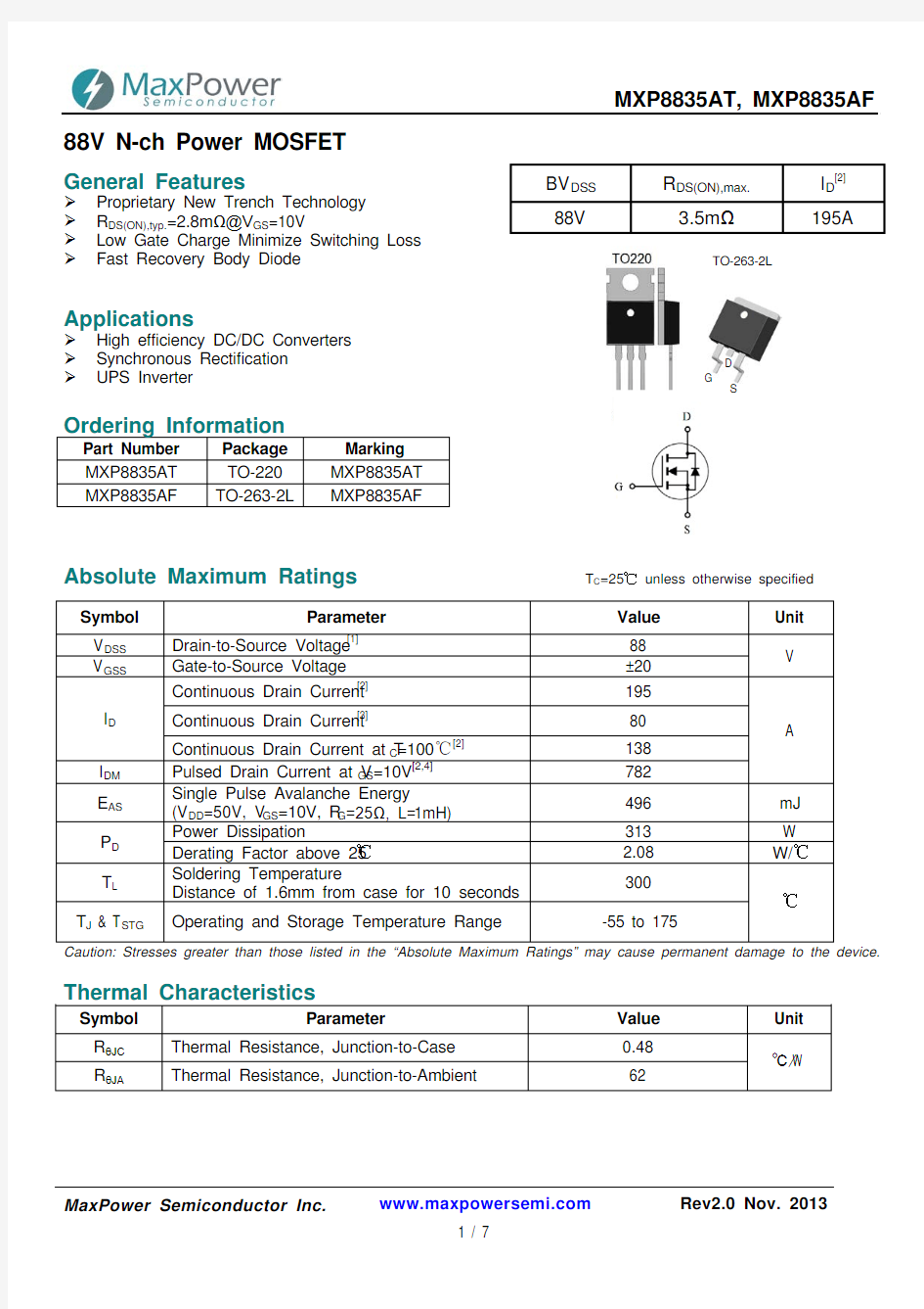
Ordering Information
Part Number Package Marking MXP8835AT TO-220 MXP8835AT MXP8835AF
TO-263-2L MXP8835AF
Absolute Maximum Ratings
T C =25℃ unless otherwise specified
Symbol Parameter Value Unit V DSS Drain-to-Source Voltage [1] 88 V
V GSS Gate-to-Source Voltage ±20 I D Continuous Drain Current [2] 195 A
Continuous Drain Current [3]
80 Continuous Drain Current at T C =100℃[2]
138 I DM Pulsed Drain Current at V GS =10V [2,4]
782 E AS Single Pulse Avalanche Energy
(V DD =50V, V GS =10V, R G =25?, L=1mH) 496 mJ P D Power Dissipation
313 W Derating Factor above 25℃ 2.08 W/℃ T L Soldering Temperature
Distance of 1.6mm from case for 10 seconds 300
℃
T J & T STG
Operating and Storage Temperature Range
-55 to 175
Caution: Stresses greater than those listed in the “Absolute Maximum Ratings” may cause permanent damage to the device.
Thermal Characteristics
Symbol Parameter
Value Unit R θJC Thermal Resistance, Junction-to-Case 0.48 ℃/W
R θJA
Thermal Resistance, Junction-to-Ambient
62
TO-263-2L
G
S
D
OFF Characteristics T J =25℃ unless otherwise specified Symbol Parameter Min. Typ. Max. Unit Test Conditions BV DSS Drain-to-Source Breakdown Voltage 88 V V GS=0V, I D=250uA
I DSS Drain-to-Source Leakage Current 5 uA V DS=88V, V GS=0V
I GSS Gate-to-Source Leakage Current ±100 nA V GS=±20V, V DS=0V ON Characteristics T J =25℃ unless otherwise specified Symbol Parameter Min. Typ. Max. Unit Test Conditions
R DS(ON)Static Drain-to-Source
On-Resistance
-- 2.8 3.5 m?V GS=10V, I D=80A[5]
V GS(TH)Gate Threshold Voltage 2.0 -- 4.0 V V DS = V GS, I D=250uA g FS Forward Transconductance -- 160 -- S V DS =10V, I D=80A[5] Dynamic Characteristics Essentially independent of operating temperature Symbol Parameter Min. Typ. Max. Unit Test Conditions
C iss Input Capacitance 14.3
nF V GS=0V, V DS=25V, f=1.0MH Z
C rss Reverse Transfer Capacitance 0.36
C oss Output Capacitance 0.97
R G Gate Series Resistance 1.95 ?f=1.0MH Z
Q g Total Gate Charge 149
nC
V DD=40V,
I D=80A, V GS=10V
Q gs Gate-to-Source Charge 46
Q gd Gate-to-Drain (Miller) Charge 41
Resistive Switching Characteristics Essentially independent of operating temperature Symbol Parameter Min. Typ. Max. Unit Test Conditions
t d(on)Turn-on Delay Time 52
ns V DD=40V I D=40A V GS=10V R G=10?
t rise Rise Time 126
t d(off)Turn-off Delay Time 155
t fall Fall Time 94
Source-Drain Body Diode Characteristics T J=25℃ unless otherwise specified Symbol Parameter Min Typ. Max. Unit Test Conditions I SD Continuous Source Current[2]195
A Maximum Ratings I SM Pulsed Source Current[2]782
V SD Diode Forward Voltage 0.90 1.2 V I S=80A, V GS=0V
t rr Reverse Recovery Time 90 ns V
GS =0V
I F=80A,di/dt=100A/μs
Q rr Reverse Recovery Charge 155 nC
Note:
[1] T J=+25℃ to +175℃
[2] Silicon limited current only
[3] Package limited current
[4] Repetitive rating, pulse width limited by both maximum junction temperature.
[5] Pulse width≤380μs; duty cycle≤2%.
MaxPower Semiconductor https://www.doczj.com/doc/0e14851437.html, Rev2.0 Nov. 2013
MaxPower Semiconductor Inc. https://www.doczj.com/doc/0e14851437.html, Rev2.0 Nov. 2013
MaxPower Semiconductor Inc.
https://www.doczj.com/doc/0e14851437.html, Rev2.0 Nov. 2013
MaxPower Semiconductor Inc.
https://www.doczj.com/doc/0e14851437.html, Rev2.0 Nov. 2013
Package Dimensions
TO-220-3L
MaxPower Semiconductor https://www.doczj.com/doc/0e14851437.html, Rev2.0 Nov. 2013
TO-263-2L
MaxPower Semiconductor https://www.doczj.com/doc/0e14851437.html, Rev2.0 Nov. 2013