.
.
飛虹積體電路股份有限公司 Page 1 of 11
F EATURES
? 4 wires PS/II interface built-in.
? CMOS technology for lower power consumption. ? Fully compatible with IBM PS/II series PC.
? Supports four working modes: Reset, Stream, Remote and Wrap. ? 16 commands plus acknowledgment code.
? 7 different sample rates from 10/sec to 200/sec. ? 4 different resolutions: 1, 2, 4 and 8 count/mm. ? Scaling can be set to 2:1 as specified by IBM spec. ? Reduced external component counts by chip integration.
? RC oscillation.
? Built-in X/Y independent Auto-Ref function (E-CMOS Patented):X/Y threshold voltage level track with input signal dynamically and independently. ? High standard ESD and EFT immunity.
G ENERAL D ESCRIPTION
EC3592R is a single chip PS/II Mouse Controller, designed and fabricated in CMOS Technology. The EC3592R is available in 14-pin or 16-pin P-DIP package.
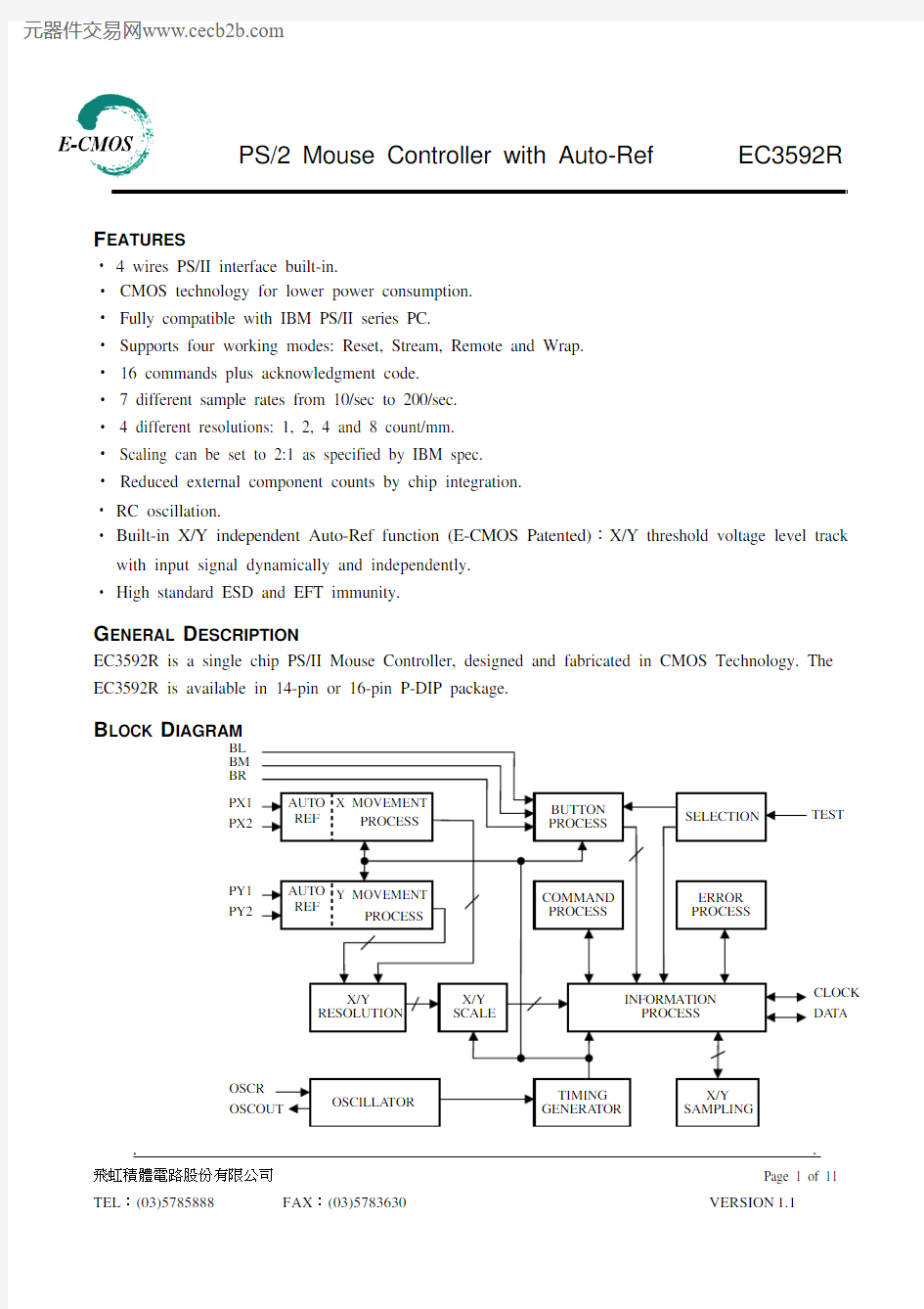
B LOCK D IAGRAM
BL BM BR PX1PX2
PY1PY2
TEST
CLOCK DA TA
.
.
飛虹積體電路股份有限公司 Page 2 of 11
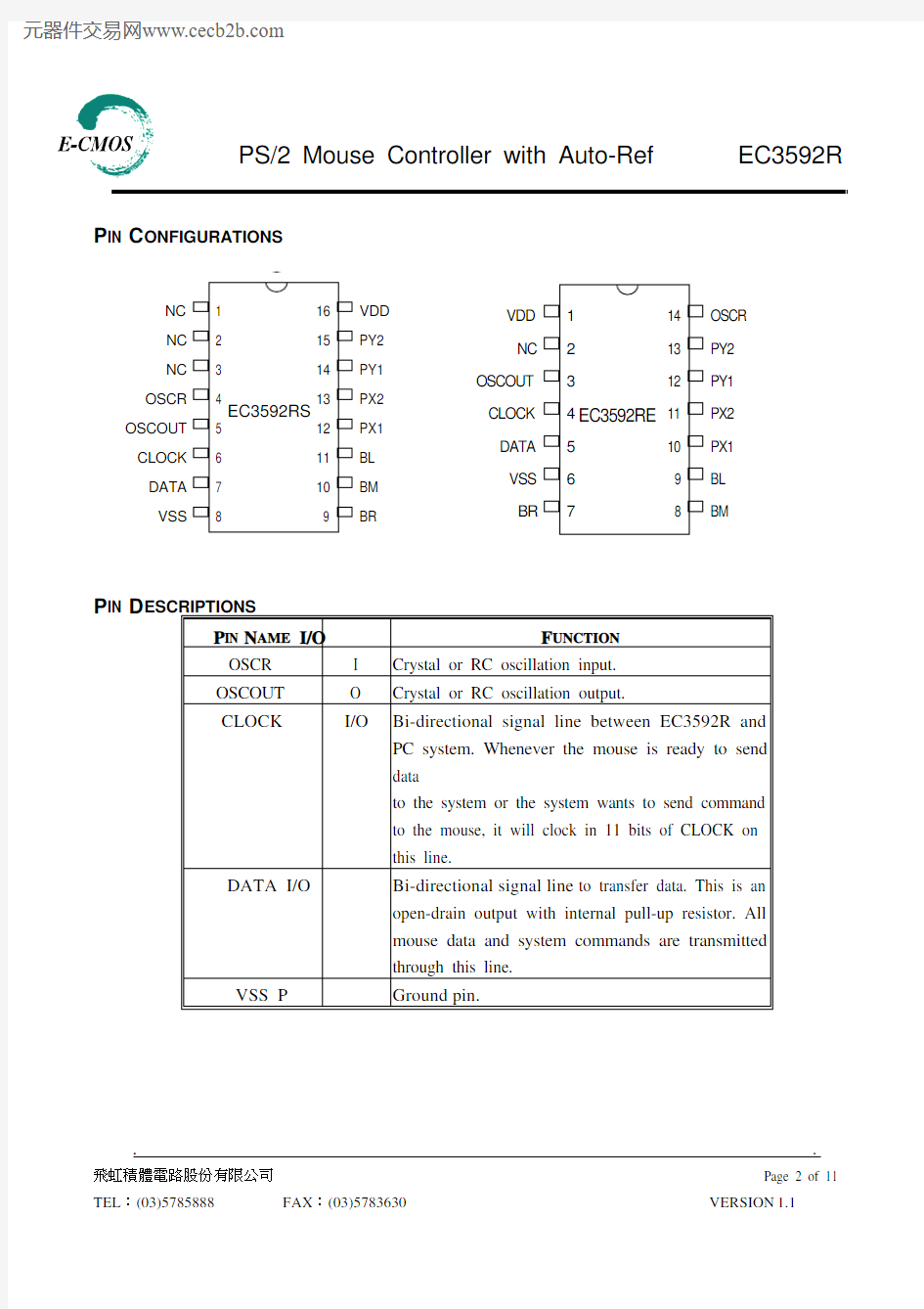
P IN C ONFIGURATIONS
NC OSCOUT CLOCK DATA VSS
VDD PY2 PY1 PX2 PX1 BL BM BR
NC
OSCR NC
P IN D ESCRIPTIONS
P IN N AME I/O F UNCTION
OSCR I Crystal or RC oscillation input. OSCOUT O
Crystal or RC oscillation output.
CLOCK
I/O Bi-directional signal line between EC3592R and
PC system. Whenever the mouse is ready to send
data
to the system or the system wants to send command to the mouse, it will clock in 11 bits of CLOCK on this line.
DATA I/O Bi-directional signal line to transfer data. This is an
open-drain output with internal pull-up resistor. All
mouse data and system commands are transmitted through this line.
VSS P Ground pin.
.
.
飛虹積體電路股份有限公司 Page 3 of 11
P IN N AME I/O F UNCTION
BR
I
Right button selection. Built-in pull-down resistor of 50K ΩBR pin is HIGH when right button is pressed and becomes LOW when it is released. EC3592R has edge-triggered button operation. It will only report through DATA line on a rising edge or falling edge of the input signal.
BM I
Middle button selection. Built-in pull-down resistor
of 50K Ω. It is also edge-triggered button operation as “BR”.
BL
I
Left button selection. Built-in pull-down resistor of 50K Ω. It is also edge-triggered button operation as “BR”.
PX1 I Input from the first X-axis photo-encoder.
PX2
I
Input from the second X-axis photo- encoder. PX1 and PX2 constitute positive (negative) counts for rightward (leftward) movement on the screen.
PY1 I Input from the first Y-axis photo-encoder. PY2
I
Input from the second Y-axis photo-encoder. PY1 and PY2 constitute positive (negative) counts for downward (upward) movement on the screen.
VDD
P
+5V power supply.
A BSOLUTE M AXIMUM R ATINGS
P ARAMETER S YMBOL M IN . M AX . U NIT Supply Voltage Vdd 0 6.5 V Ambient Temperature Tamb 0 70 ℃ Storage Temperature Tstg
-40
125
℃
Power Dissipation (Temp. = 70 ℃)
Pd 100 mW
Note: This is a stress rating only and functional operation of the device at these or at any other conditions above those indicated in the operational sections of this specification is not implied. Exposure to absolute
.
.
飛虹積體電路股份有限公司 Page 4 of 11
maximum rating may affect device reliability.
DC E LECTRICAL C HARACTERISTICS
(N OTE : V DD =5V, UNLESS OTHERWISE SPECIFIED )
P ARAMETER
S YMBOL M IN . T YP . M AX . U NIT Operating Voltage Vdd 4.5 5 5.5 V Operating current (No load) Iop 1.0 2.5 mA PX1/PX2/PY1/PY2 Input range Vir 0.1 3.2 V PX1/PX2/PY1/PY2 Input amplitude Via 0.6 V
PX1/PX2/PY1/PY2 Internal Resistor Rpxy 12 K Ω BL/BM/BR Input High Voltage Vih 3.2 V
BL/BM/BR Input Low Voltage Vil
1.3
V BL/BM/BR Internal Pull-down Resistor
Rbut 50
K Ω CLOCK/DATA Output Current (Vol. =0.5V)
Iol 8 mA
CLOCK/DATA Internal Pull-up Resistor
Rcd 5 K Ω PX1/PX2/PY1/PY2/BL/BM/BR Input Leakage Current (Vih = 5V)
Iih 2 uA
AC E LECTRICAL C HARACTERISTICS
P ARAMETER S YMBOL
M IN . T YP . M AX . U NIT
Oscillator Frequency
R=270 K Ω Foscr 62 75 90 KHz BL/BM/BR Button Debounce Time
Tbd
43
ms
.
.
飛虹積體電路股份有限公司 Page 5 of 11
T IMING D IAGRAM
Mouse sends data out:
T3T4
Bit
Parity Bit
T2
T1
Bit 0Bit 1
1st
2nd
3rd
10th
11th
CLOCK DATA
Stop Bit
Clock
Mouse receive data:
T5T6
Start Bit
Parity Bit
T7
Bit 0
1st
2nd
10th 11th CLOCK DATA
Stop Bit
9th
T9
T8
Clock
Line-control Bit
IBM SPEC E-CMOS SPEC T1 Time from DATA transition to the falling edge of
CLOCK. 5~25 13.3 T2 Time from the rising edge of CLOCK to DATA
transition. 5~(T4-5) 26.7
T3 Duration of CLOCK Low. 30~50 40 T4 Duration of CLOCK High. 30~50 40 T5 Duration of CLOCK Low. 30~50 40 T6
Duration of CLOCK High.
30~50
40
T7 Time from the rising edge of CLOCK to DATA
sampled point. 5~25 13.3 T8 Time from the rising edge of the 10th CLOCK to
starting point of line-control bit. 13.3 T9 The pulse width of line-control bit.
80
(Base on oscillator frequency=70KHz)
(Unit in μs)
.
.
飛虹積體電路股份有限公司 Page 6 of 11
PS/2 C OMMAND L IST
H EX C ODE
C OMMAN
D EC3592’S R ESPONSE
FF Reset FA, AA, 00 FE Resend XX, (XX, XX) F6 Set Default FA F5 Disable FA F4 Enable FA F3, XX Set Sampling Rate FA, FA F2
Read Device Type
FA, 00 F0 Set Remote Mode FA EE Set Wrap Mode FA EC Reset Wrap Mode FA EB Read Data FA, XX, XX, XX
EA Set Stream Mode FA E9 Status Request FA, XX, XX, XX
E8, XX
Set Resolution
FA, FA
E7 Set Scaling 2:1 FA E6 Reset Scaling
FA
A. F3, XX S ET S AMPLING R ATE
S ECOND B YTE XX
S AMPLING R ATE
0A 10/sec. 14 20/sec. 28 40/sec. 3C 60/sec. 50 80/sec. 64 100/sec. C8 200/sec.
.
.
飛虹積體電路股份有限公司 Page 7 of 11
B. E9 S TATUS R EQUEST
B YTE B IT D ESCRIPTION
3 0-7 Current Sampling Rate (Bit 0=LSB) 2 0-7 Current Sampling Setting (Bit 0=LSB)
1 7
Reserved
6 0 = Stream Mode, 1 = Remote Mode
5 0 = Disabled, 1 = Enabled 4 0 = Scaling 1:1, 1 = Scaling 2:1
3 Reserved 2 1= Left Button Pressed
1
Reserved
1 = Right Button Pressed
C. E8, XX S ET R ESOLUTION
S ECOND B YTE XX R ESOLUTION (C OUNTS PER MM)
00 1 01 2 02 4 03 8
D. E7 S ET S CALING 2:1
I NPUT
O UTPUT
0 0 1 1 2 1 3 3 4 6 5 9 N (≧6) 2.0×N
.
.
飛虹積體電路股份有限公司 Page 8 of 11
I NPUT /O UTPUT E QUIVALENT C IRCUIT
.
.
飛虹積體電路股份有限公司 Page 9 of 11
. .
飛虹積體電路股份有限公司 Page 10 of 11
A PPLICATION C IRCUITS
(Note: This application circuit is for reference only)
VCC
DATA CLOCK
GND
P S /2 M o u s e C o n t r o l l e r w i t h A u t o -R e f E C 3592R
.
.
虹積體電路股份有限公司 P a g e 11 o f 11
L :(03)5785888 F A X :(03)5783630 V E R S I O N 1.1
0?
N 3904
(*)Y 1 I S A C E R A M I C R E S O N A T O R S U C H A S C S A 18.43M X Z 040
(F R O M M U R A T A ) O R K B R -18.43-M S A (F R O M A V X ).T y p i c a l A p p l i c a t i o n C i r c u i t F o r H D N S -2000 O p t i c a l I n p u t (F o r R e f e r e n c e O n l y )