FEATURES
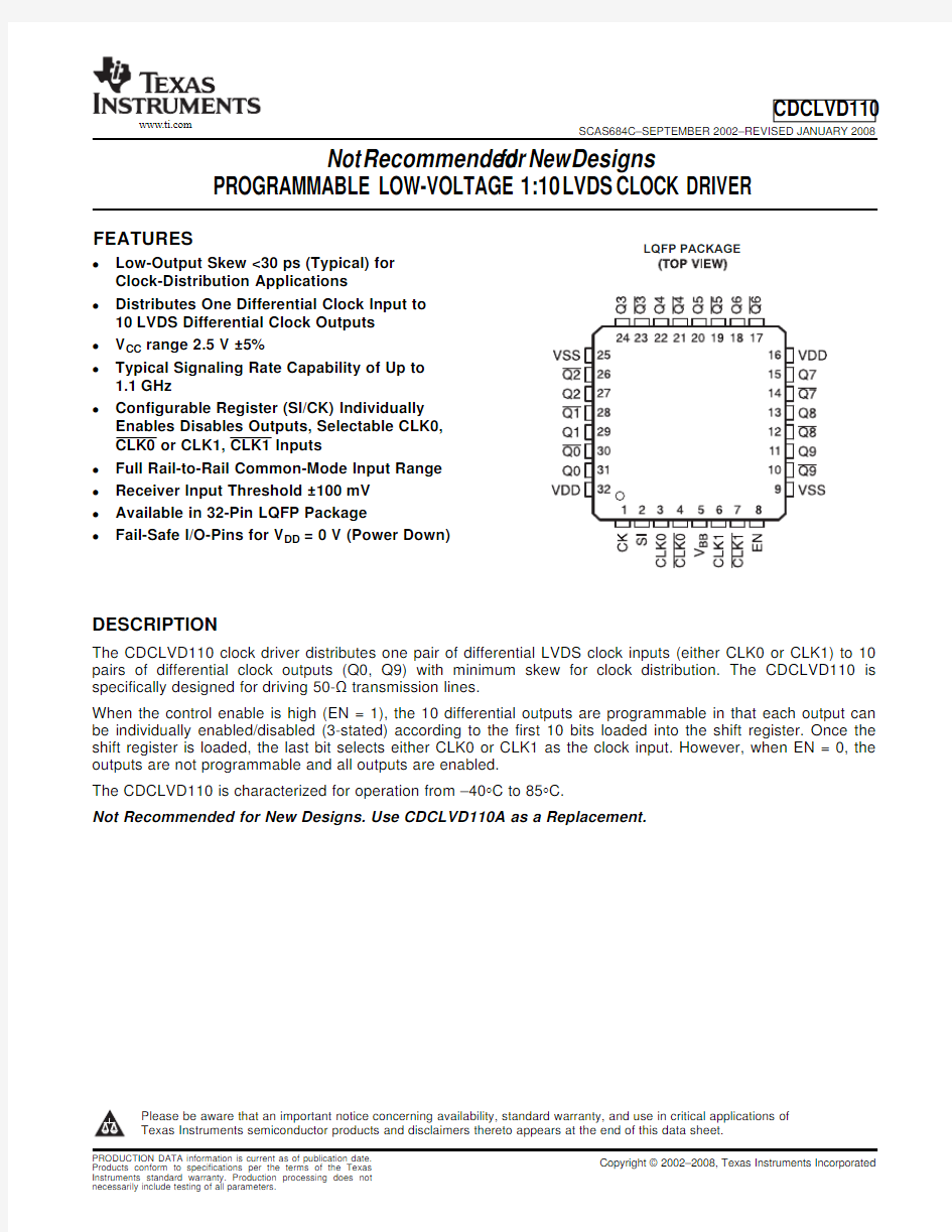
LQFP PACKAGE
DESCRIPTION
CDCLVD110
SCAS684C–SEPTEMBER 2002–REVISED JANUARY 2008
https://www.doczj.com/doc/3d5090181.html,
Not Recommended for New Designs
PROGRAMMABLE LOW-VOLTAGE 1:10LVDS CLOCK DRIVER
?Low-Output Skew <30ps (Typical)for Clock-Distribution Applications
?Distributes One Differential Clock Input to 10LVDS Differential Clock Outputs ?V CC range 2.5V ±5%
?Typical Signaling Rate Capability of Up to 1.1GHz
?
Configurable Register (SI/CK)Individually Enables Disables Outputs,Selectable CLK0,CLK0or CLK1,CLK1Inputs
?Full Rail-to-Rail Common-Mode Input Range ?Receiver Input Threshold ±100mV ?Available in 32-Pin LQFP Package
?
Fail-Safe I/O-Pins for V DD =0V (Power Down)
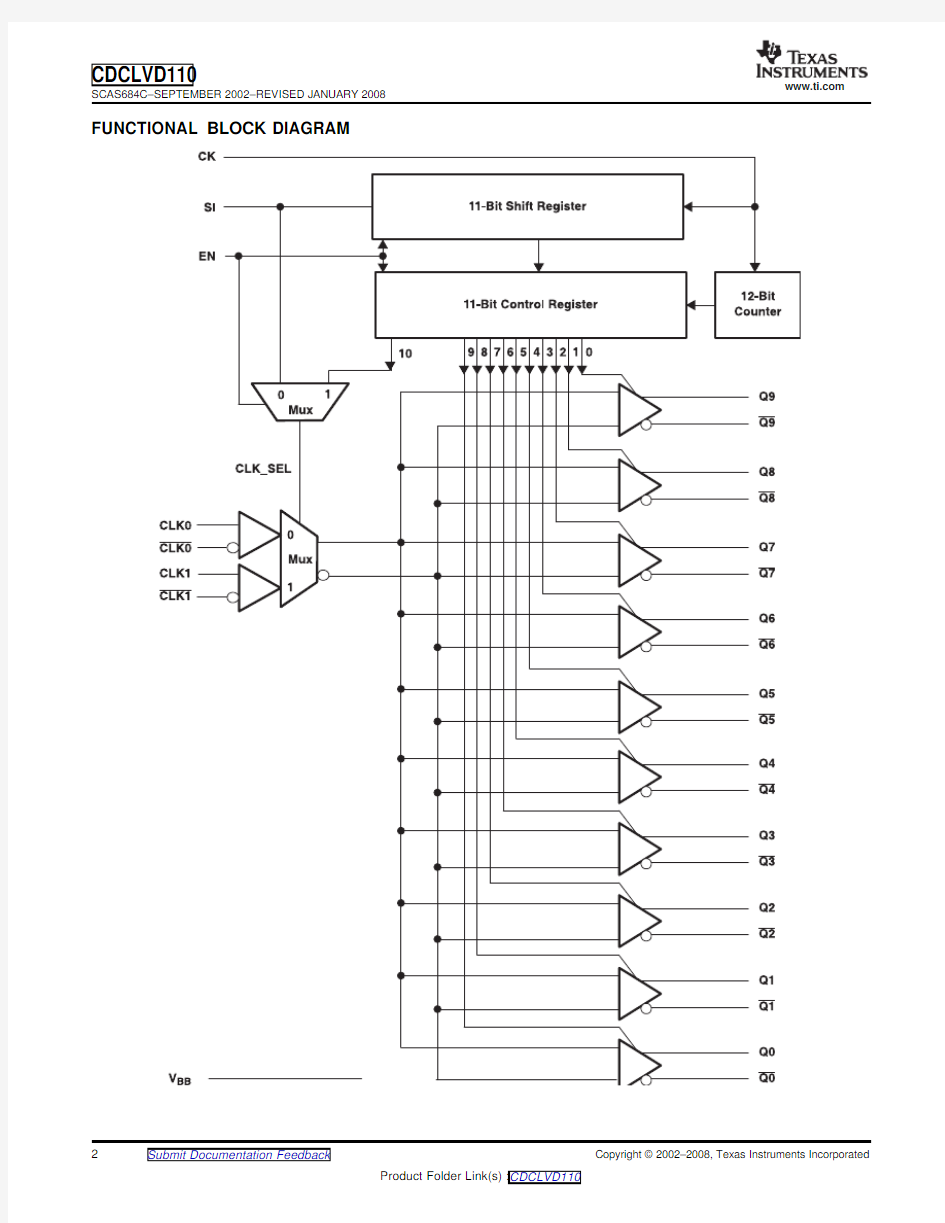
The CDCLVD110clock driver distributes one pair of differential LVDS clock inputs (either CLK0or CLK1)to 10pairs of differential clock outputs (Q0,Q9)with minimum skew for clock distribution.The CDCLVD110is specifically designed for driving 50-?transmission lines.
When the control enable is high (EN =1),the 10differential outputs are programmable in that each output can be individually enabled/disabled (3-stated)according to the first 10bits loaded into the shift register.Once the shift register is loaded,the last bit selects either CLK0or CLK1as the clock input.However,when EN =0,the outputs are not programmable and all outputs are enabled.
The CDCLVD110is characterized for operation from –40°C to 85°C.
Not Recommended for New https://www.doczj.com/doc/3d5090181.html,e CDCLVD110A as a Replacement.
Please be aware that an important notice concerning availability,standard warranty,and use in critical applications of Texas Instruments semiconductor products and disclaimers thereto appears at the end of this data sheet.
https://www.doczj.com/doc/3d5090181.html,
FUNCTIONAL BLOCK
DIAGRAM
CDCLVD110
SCAS684C–SEPTEMBER 2002–REVISED JANUARY 2008
https://www.doczj.com/doc/3d5090181.html,
ABSOLUTE MAXIMUM RATINGS(1) RECOMMENDED OPERATING CONDITIONS ELECTRICAL CHARACTERISTICS
CDCLVD110 SCAS684C–SEPTEMBER2002–REVISED JANUARY2008
TERMINAL FUNCTIONS
TERMINAL
I/O DESCRIPTION
NAME NO.
CK1I Control register input clock,features a120-k?pullup resistor
SI2I Control register serial input/CLK Select,features a120-k?pulldown resistor
CLK03I True differential input,LVDS
CLK04I Complementary differential input,LVDS
V BB5O Reference voltage output
CLK16I True differential input,LVDS
CLK17I Complementary differential input,LVDS
EN8I Control enable(for programmability),features a120-k?pulldown resistor,input
V SS9,25Device ground
V DD16,32Supply voltage
11,13,15,18,20,22,
Q[9:0]O Clock outputs,these outputs provide low-skew copies of CLKIN
24,27,29,31
10,12,14,17,19,
Q[9:0]O Complementary clock outputs,these outputs provide low-skew copies of CLKIN 21,23,26,28,30
VALUE UNIT V DD Supply voltage–0.3to2.8V
V I Input voltage–0.2to(V DD+0.2)V
V O VI Output voltage–0.2to(V DD+0.2)V Qn,Qn,I OSD Driver short circuit current Continuous
Electrostatic discharge(HBM1.5k?,100pF),ESD>2000V (1)Stresses beyond those listed under absolute maximum ratings may cause permanent damage to the device.These are stress ratings
only,and functional operation of the device at these or any other conditions beyond those indicated under recommended operating conditions is not implied.Exposure to absolute-maximum-rated conditions for extended periods may affect device reliability.
MIN NOM MAX UNIT V DD Supply voltage 2.375 2.5 2.625V V IC Receiver common-mode input voltage0.5|V ID|V DD–0.5|V ID|V T A Operating free-air temperature–4085°C
over recommended operating free-air temperature range(unless otherwise noted)
PARAMETER TEST CONDITIONS MIN TYP MAX UNIT DRIVER
|V OD|Differential output voltage R L=100?250450600mV ΔV OD V OD magnitude change50mV V OS Offset voltage–40°C to85°C0.95 1.2 1.45V ΔV OS V OS magnitude change350mV
V O=0V–20
I OS Output short circuit current mA
|V OD|=0V20
V BB Reference output voltage V DD=2.5V,I BB=–100μA 1.15 1.25 1.35V C O Output capacitance V O=V DD or GND3pF
https://www.doczj.com/doc/3d5090181.html,
JITTER CHARACTERISTICS
LVDS —SWITCHING CHARACTERISTICS
CONTROL REGISTER CHARACTERISTICS
CDCLVD110
SCAS684C–SEPTEMBER 2002–REVISED JANUARY 2008
ELECTRICAL CHARACTERISTICS (continued)
over recommended operating free-air temperature range (unless otherwise noted)
PARAMETER
TEST CONDITIONS
MIN
TYP MAX
UNIT
RECEIVER V IDH Input threshold high 100
mV V IDL Input threshold low –100mV |V ID |Input differential voltage
200mV I IH V I =V DD Input current,CLK0/CLK0,CLK1/CLK1–5
5μA I IL V I =0V C I
Input capacitance
V I =V DD or GND
3
pF
SUPPLY CURRENT Full loaded
All outputs enabled and loaded,R L =100?,f =0Hz 130I DD Supply current
No load Outputs enabled,no output load,f =0Hz 35mA I DDZ
3-State
All outputs 3-state by control logic,f =0Hz
35
characterized with CDCLVD110performance EVM,V DD =3.3V,OUTPUTS NOT UNDER TEST are terminated to 50?
PARAMETER
TEST CONDITIONS
MIN
TYP MAX
UNIT 12kHz to 5MHz,f out =30.72MHz 650Additive phase jitter from input to t jitterLVDS
fs rms
LVDS output Q3and Q3
12kHz to 20MHz,f out =125MHz
299
over recommended operating free-air temperature range,V DD =2.5V ±5%
FROM TO PARAMETER
MIN
TYP MAX
UNIT (INPUT)(OUTPUT)CLK0,CLK0t PLH Propagation delay low-to-high Qn,Qn 23ns CLK1,CLK1Propagation delay high-to-low CLK0,CLK0t PHL Qn,Qn 2
3ns
CLK1,CLK1CLK0,CLK0t duty Duty cycle Qn,Qn 45%
55%
CLK1,CLK1
t sk(o)Output skew Any Qn,Qn 30
ps t sk(p)Pulse skew
Any Qn,Qn 50ps t sk(pp)Part-to-part skew
Any Qn,Qn 600ps t r Output rise time,20%to 80%,R L =100?,C L =5pF Any Qn,Qn 350ps t f Output fall time,20%to 80%,R L =100?,C L =5pF Any Qn,Qn 350
ps CLK0,CLK0f clk
Max input frequency
Any Qn,Qn
900
1100
MHz CLK1,CLK1over recommended operating free-air temperature range,V DD =2.5V ±5%(unless otherwise noted)
PARAMETER
TEST CONDITIONS
MIN TYP MAX
UNIT f MAX Maximum frequency of shift register 100
150
MHz t su Setup time,clock to SI 2ns t h Hold time,clock to SI 1.5ns t removal Removal time,enable to clock 1.5ns t w Clock pulse width,minimum 3ns V IH Logic input high V DD =2.5V 2
V V IL
Logic input low
V DD =2.5V
0.8
V
https://www.doczj.com/doc/3d5090181.html,
SPECIFICATION OF CONTROL REGISTER
CDCLVD110 SCAS684C–SEPTEMBER2002–REVISED JANUARY2008
CONTROL REGISTER CHARACTERISTICS(continued)
over recommended operating free-air temperature range,V DD=2.5V±5%(unless otherwise noted)
PARAMETER TEST CONDITIONS MIN TYP MAX UNIT Input current,CK pin–55
I IH V I=V DDμA
Input current,SI and EN pins10–30
Input current,CK pin–1030
I IL V I=GNDμA
Input current,SI and EN pins–55
The CDCLVD110is provided with an11-bit,serial-in shift register and an11-bit control register.The control Register enables/disables each output clock and selects either CLK0or CLK1as the input clock.The CDCLVD110has two modes of operation:
Programmable Mode(EN=1)
The shift register utilizes a serial input(SI)and a clock input(CK).Once the shift register is loaded with11 clock pulses,the twelfth clock pulse loads the control register.The first bit(bit0)on SI enables the Q9,Q9 output pair,and the tenth bit(bit9)enables the Q0,Q0pair.The eleventh bit(bit10)on SI selects either CLK0or CLK1as the input clock;a bit value of0selects CLK0,whereas a bit value of1selects CLK1.To restart the control register configuration,a reset of the state machine must be done with a clock pulse on CK (shift register clock input)and EN set to low.The control register can be configured only once after each reset.
Standard Mode(EN=0)
In this mode,the CDCLVD110is not programmable and all the clock outputs are enabled.The clock input (CLK0or CLK1)is selected with the SI pin,as is shown in the table entitled control register.
STATE-MACHINE INPUTS
EN SI CK OUTPUT
L L X All outputs enabled,CLK0selected,control register disabled,default state
L H X All outputs enabled,CLK1selected,control register disabled
H L↑First stage stores L,other stage stores data of previous stage
H H First stage stores H,other stage stores data of previous stage
L X Reset of state machine,shift and control registers
CONTROL REGISTER
BIT10BITS[0-9]Q N[0-9]
L H CLK0
H H CLK1
X L Outputs disabled
SERIAL INPUT(SI)SEQUENCE
BIT10BIT9BIT8BIT7BIT6BIT5BIT4BIT3BIT2BIT1BIT0 CLK_SEL Q0Q1Q2Q3Q4Q5Q6Q7Q8Q9 TRUTH TABLE FOR CONTROL LOGIC
CK EN SI CLK0CLK0CLK1CLK1Q(0-9)Q(0-9) L L L L H X X L H
L L L H L X X H L
L L L Open Open X X L H
L L H X X L H L H
L L H X X H L H L
L L H X X Open Open L H All outputs enabled X=Don't care
https://www.doczj.com/doc/3d5090181.html,
APPLICATION INFORMATION
Fall-Safe Information
LVDS Receiver Input Termination
Control Inputs Termination
CDCLVD110
SCAS684C–SEPTEMBER 2002–REVISED JANUARY 2008
For V DD =0V (power-down mode)the CDCLVD110has fail-safe input and output pins.In power-on mode,fail-safe biasing at input pins can be accomplished with a 10-k ?pullup resistor from CLK0/CLK1to VDD and a 10-k ?pulldown resistor from CLK0/CLK1to GND.
The LVDS receiver inputs need to have 100-?termination resistors placed as close as possible across the input pins.
No external termination is required.The CK control input has an internal 120-k.pullup resistor while SI-and EN-control inputs each have an internal 120-k ?pulldown resistor.If the control pins are left open per the default,all outputs are enabled,CLK0,CLK0is selected,and the control register is disabled.
https://www.doczj.com/doc/3d5090181.html,
PARAMETER MEASUREMENT
INFORMATION
CDCLVD110
SCAS684C–SEPTEMBER 2002–REVISED JANUARY 2008
A.
Output skew,t sk(o),is calculated as the greater of:
–The difference between the fastest and the slowest t PLHn (n =1,2,...10)–The difference between the fastest and the slowest t PHLn (n =1,2,...10)
B.
Part-to-part skew,t sk(pp),is calculated as the greater of:
–The difference between the fastest and the slowest t PLHn (n =1,2,...10)across multiple devices –The difference between the fastest and the slowest t PHLn (n =1,2,...10)across multiple devices
C.
Pulse skew,t sk(p),is calculated as the magnitude of the absolute time difference between the high-to-low (t PHL )and the low-to-high (t PLH )propagation delays when a single switching input causes one or more outputs to switch,t sk(p)=|t PHL –t PLH |.Pulse skew is sometimes referred to as pulse width distortion or duty cycle skew.
Figure 1.Waveforms for Calculation of t sk(o)and t sk(pp)
https://www.doczj.com/doc/3d5090181.html,
CDCLVD110
SCAS684C–SEPTEMBER 2002–REVISED JANUARY 2008
PARAMETER MEASUREMENT INFORMATION (continued)
Figure 2.Test Criteria for f clk ,Duty Cycle,t r ,t f ,V OD
PACKAGING INFORMATION
Orderable Device Status (1)Package Type Package Drawing Pins Package Qty Eco Plan (2)
Lead/Ball Finish MSL Peak Temp (3)CDCLVD110VF NRND LQFP VF 32250Green (RoHS &no Sb/Br)CU NIPDAU Level-1-260C-UNLIM CDCLVD110VFG4NRND LQFP VF 32250
Green (RoHS &no Sb/Br)
CU NIPDAU Level-1-260C-UNLIM CDCLVD110VFR NRND LQFP VF 321000Green (RoHS &
no Sb/Br)CU NIPDAU Level-1-260C-UNLIM CDCLVD110VFRG4
NRND
LQFP
VF
32
1000Green (RoHS &
no Sb/Br)
CU NIPDAU
Level-1-260C-UNLIM
(1)
The marketing status values are defined as follows:ACTIVE:Product device recommended for new designs.
LIFEBUY:TI has announced that the device will be discontinued,and a lifetime-buy period is in effect.
NRND:Not recommended for new designs.Device is in production to support existing customers,but TI does not recommend using this part in a new design.
PREVIEW:Device has been announced but is not in production.Samples may or may not be available.OBSOLETE:TI has discontinued the production of the device.
(2)
Eco Plan -The planned eco-friendly classification:Pb-Free (RoHS),Pb-Free (RoHS Exempt),or Green (RoHS &no Sb/Br)-please check https://www.doczj.com/doc/3d5090181.html,/productcontent for the latest availability information and additional product content details.TBD:The Pb-Free/Green conversion plan has not been defined.
Pb-Free (RoHS):TI's terms "Lead-Free"or "Pb-Free"mean semiconductor products that are compatible with the current RoHS requirements for all 6substances,including the requirement that lead not exceed 0.1%by weight in homogeneous materials.Where designed to be soldered at high temperatures,TI Pb-Free products are suitable for use in specified lead-free processes.
Pb-Free (RoHS Exempt):This component has a RoHS exemption for either 1)lead-based flip-chip solder bumps used between the die and package,or 2)lead-based die adhesive used between the die and leadframe.The component is otherwise considered Pb-Free (RoHS compatible)as defined above.
Green (RoHS &no Sb/Br):TI defines "Green"to mean Pb-Free (RoHS compatible),and free of Bromine (Br)and Antimony (Sb)based flame retardants (Br or Sb do not exceed 0.1%by weight in homogeneous material)
(3)
MSL,Peak Temp.--The Moisture Sensitivity Level rating according to the JEDEC industry standard classifications,and peak solder temperature.
Important Information and Disclaimer:The information provided on this page represents TI's knowledge and belief as of the date that it is provided.TI bases its knowledge and
belief on information provided by third parties,and makes no representation or warranty as to the accuracy of such information.Efforts are underway to better integrate information from third parties.TI has taken and continues to take reasonable steps to provide representative and accurate information but may not have conducted destructive testing or chemical analysis on incoming materials and chemicals.TI and TI suppliers consider certain information to be proprietary,and thus CAS numbers and other limited information may not be available for release.
In no event shall TI's liability arising out of such information exceed the total purchase price of the TI part(s)at issue in this document sold by TI to Customer on an annual basis.
PACKAGE OPTION ADDENDUM
https://www.doczj.com/doc/3d5090181.html,
4-Aug-2009
TAPE AND REEL
INFORMATION
*All
dimensions are nominal
Device
Package Type Package Drawing Pins SPQ
Reel Diameter (mm)Reel Width W1(mm)A0(mm)B0(mm)K0(mm)P1(mm)W (mm)Pin1Quadrant CDCLVD110VFR LQFP
VF
32
1000
330.0
16.4
9.6
9.6
1.9
12.0
16.0
Q2
PACKAGE MATERIALS INFORMATION
https://www.doczj.com/doc/3d5090181.html,
3-Mar-2012
分销商库存信息:
TI
CDCLVD110VFR CDCLVD110VFRG4CDCLVD110VFG4 CDCLVD110VF