1/4.5-Inch 1.6Mp CMOS Digital Image Sensor MT9M002
For the latest MT9M002 data sheet, refer to Aptina’s Web site: https://www.doczj.com/doc/3c10835768.html,
Features
?DigitalClarity? CMOS imaging technology ?Maximum frame rate (1284H x812V/60fps at 99 MHz)
?Superior low-light performance
?Low dark current
?Global reset release (GRR), which starts the exposure of all rows simultaneously
?Simple two-wire serial interface
?Programmable controls: gain, frame rate, frame size, exposure
?Horizontal and vertical mirror image
?Automatic black level calibration
?On-chip phase-locked loop (PLL) oscillator
?Bulb exposure mode for arbitrary exposure times ?Snapshot mode to take frames on demand ?Parallel data output
?Electronic rolling shutter (ERS), progressive scan ?Programmable power-down mode (mode A or mode B)
?Xenon and LED flash support with fast exposure adaptation
?Flexible support for mechanical shutter Applications
?720p high-definition digital video camcorder ?Solid state (flash) pocket DVC
?Digital still cameras
?PC cameras
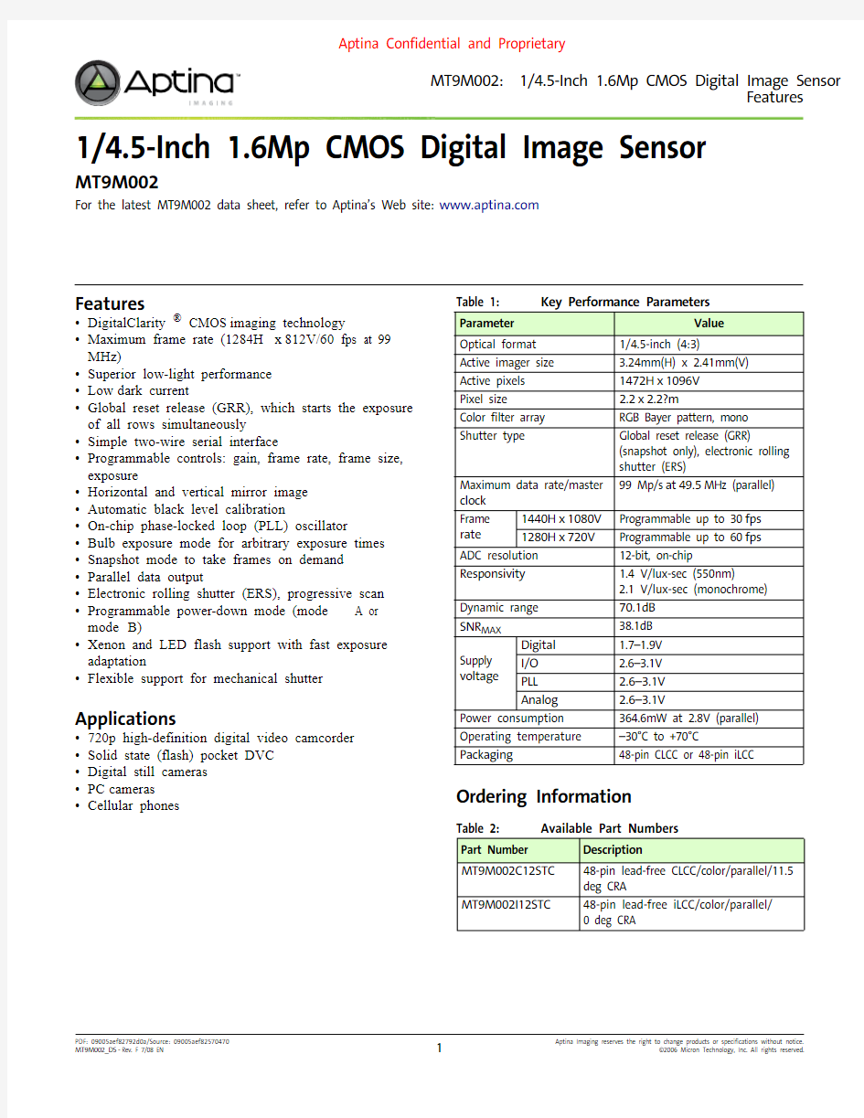
?Cellular phones Table 1: Key Performance Parameters
Ordering Information
Table 2: Available Part Numbers
Parameter Value
Optical format1/4.5-inch (4:3)
Active imager size 3.24mm(H) x 2.41mm(V)
Active pixels1472H x1096V
Pixel size 2.2x2.2?m
Color filter array RGB Bayer pattern, mono Shutter type Global reset release (GRR)
(snapshot only), electronic rolling
shutter (ERS)
Maximum data rate/master
clock
99 Mp/s at49.5MHz (parallel)
Frame
rate
1440H x1080V Programmable up to 30fps
1280H x720V Programmable up to 60fps
ADC resolution12-bit, on-chip
Responsivity 1.4 V/lux-sec (550nm)
2.1 V/lux-sec (monochrome) Dynamic range70.1dB
SNR MAX38.1dB
Supply
voltage
Digital 1.7–1.9V
I/O 2.6–3.1V
PLL 2.6–3.1V
Analog 2.6–3.1V
Power consumption364.6mW at 2.8V (parallel) Operating temperature–30°C to +70°C
Packaging48-pin CLCC or 48-pin iLCC
Part Number Description
MT9M002C12STC48-pin lead-free CLCC/color/parallel/11.5
deg CRA
MT9M002I12STC48-pin lead-free iLCC/color/parallel/
0 deg CRA
Table of Contents
Features. . . . . . . . . . . . . . . . . . . . . . . . . . . . . . . . . . . . . . . . . . . . . . . . . . . . . . . . . . . . . . . . . . . . . . . . . . . . . . . . . . . . . . . . . . . . . .1 Applications . . . . . . . . . . . . . . . . . . . . . . . . . . . . . . . . . . . . . . . . . . . . . . . . . . . . . . . . . . . . . . . . . . . . . . . . . . . . . . . . . . . . . . . . . .1 Ordering Information. . . . . . . . . . . . . . . . . . . . . . . . . . . . . . . . . . . . . . . . . . . . . . . . . . . . . . . . . . . . . . . . . . . . . . . . . . . . . . . . . .1 General Description . . . . . . . . . . . . . . . . . . . . . . . . . . . . . . . . . . . . . . . . . . . . . . . . . . . . . . . . . . . . . . . . . . . . . . . . . . . . . . . . . . .6 Functional Overview. . . . . . . . . . . . . . . . . . . . . . . . . . . . . . . . . . . . . . . . . . . . . . . . . . . . . . . . . . . . . . . . . . . . . . . . . . . . . . . . . . .6 Signal Descriptions. . . . . . . . . . . . . . . . . . . . . . . . . . . . . . . . . . . . . . . . . . . . . . . . . . . . . . . . . . . . . . . . . . . . . . . . . . . . . . . . . . . .8 Typical Connections. . . . . . . . . . . . . . . . . . . . . . . . . . . . . . . . . . . . . . . . . . . . . . . . . . . . . . . . . . . . . . . . . . . . . . . . . . . . . . . . . .12 Pixel Array Structure. . . . . . . . . . . . . . . . . . . . . . . . . . . . . . . . . . . . . . . . . . . . . . . . . . . . . . . . . . . . . . . . . . . . . . . . . . . . . . . . . .13 Default Readout Order . . . . . . . . . . . . . . . . . . . . . . . . . . . . . . . . . . . . . . . . . . . . . . . . . . . . . . . . . . . . . . . . . . . . . . . . . . . . .13 Output Data Format. . . . . . . . . . . . . . . . . . . . . . . . . . . . . . . . . . . . . . . . . . . . . . . . . . . . . . . . . . . . . . . . . . . . . . . . . . . . . . . . . .15 Parallel Pixel Data Interface. . . . . . . . . . . . . . . . . . . . . . . . . . . . . . . . . . . . . . . . . . . . . . . . . . . . . . . . . . . . . . . . . . . . . . . . .15 Output Data Timing(Parallel Pixel Data Interface). . . . . . . . . . . . . . . . . . . . . . . . . . . . . . . . . . . . . . . . . . . . . . . . . . . . . . .16 Row Timing Details . . . . . . . . . . . . . . . . . . . . . . . . . . . . . . . . . . . . . . . . . . . . . . . . . . . . . . . . . . . . . . . . . . . . . . . . . . . . . . . .17 Serial Bus Description . . . . . . . . . . . . . . . . . . . . . . . . . . . . . . . . . . . . . . . . . . . . . . . . . . . . . . . . . . . . . . . . . . . . . . . . . . . . . . . .18 Protocol . . . . . . . . . . . . . . . . . . . . . . . . . . . . . . . . . . . . . . . . . . . . . . . . . . . . . . . . . . . . . . . . . . . . . . . . . . . . . . . . . . . . . . . . . .18 Sequence . . . . . . . . . . . . . . . . . . . . . . . . . . . . . . . . . . . . . . . . . . . . . . . . . . . . . . . . . . . . . . . . . . . . . . . . . . . . . . . . . . . . . . . . .18 Bus Idle State. . . . . . . . . . . . . . . . . . . . . . . . . . . . . . . . . . . . . . . . . . . . . . . . . . . . . . . . . . . . . . . . . . . . . . . . . . . . . . . . . . . . . .18 Start Bit. . . . . . . . . . . . . . . . . . . . . . . . . . . . . . . . . . . . . . . . . . . . . . . . . . . . . . . . . . . . . . . . . . . . . . . . . . . . . . . . . . . . . . . . . . .18 Stop Bit. . . . . . . . . . . . . . . . . . . . . . . . . . . . . . . . . . . . . . . . . . . . . . . . . . . . . . . . . . . . . . . . . . . . . . . . . . . . . . . . . . . . . . . . . . .19 Slave Address. . . . . . . . . . . . . . . . . . . . . . . . . . . . . . . . . . . . . . . . . . . . . . . . . . . . . . . . . . . . . . . . . . . . . . . . . . . . . . . . . . . . . .19 Data Bit Transfer. . . . . . . . . . . . . . . . . . . . . . . . . . . . . . . . . . . . . . . . . . . . . . . . . . . . . . . . . . . . . . . . . . . . . . . . . . . . . . . . . . .19 Acknowledge Bit. . . . . . . . . . . . . . . . . . . . . . . . . . . . . . . . . . . . . . . . . . . . . . . . . . . . . . . . . . . . . . . . . . . . . . . . . . . . . . . . . . .19 No-Acknowledge Bit . . . . . . . . . . . . . . . . . . . . . . . . . . . . . . . . . . . . . . . . . . . . . . . . . . . . . . . . . . . . . . . . . . . . . . . . . . . . . . .19 Two-Wire Serial Interface Sample Write and Read Sequences. . . . . . . . . . . . . . . . . . . . . . . . . . . . . . . . . . . . . . . . . . . . .20 16-Bit Write Sequence. . . . . . . . . . . . . . . . . . . . . . . . . . . . . . . . . . . . . . . . . . . . . . . . . . . . . . . . . . . . . . . . . . . . . . . . . . . . . .20 16-Bit Read Sequence . . . . . . . . . . . . . . . . . . . . . . . . . . . . . . . . . . . . . . . . . . . . . . . . . . . . . . . . . . . . . . . . . . . . . . . . . . . . . .20 Registers . . . . . . . . . . . . . . . . . . . . . . . . . . . . . . . . . . . . . . . . . . . . . . . . . . . . . . . . . . . . . . . . . . . . . . . . . . . . . . . . . . . . . . . . . . . .21 Register Map . . . . . . . . . . . . . . . . . . . . . . . . . . . . . . . . . . . . . . . . . . . . . . . . . . . . . . . . . . . . . . . . . . . . . . . . . . . . . . . . . . . . . .21 Register Notation . . . . . . . . . . . . . . . . . . . . . . . . . . . . . . . . . . . . . . . . . . . . . . . . . . . . . . . . . . . . . . . . . . . . . . . . . . . . . . . . . .21 Bit Fields. . . . . . . . . . . . . . . . . . . . . . . . . . . . . . . . . . . . . . . . . . . . . . . . . . . . . . . . . . . . . . . . . . . . . . . . . . . . . . . . . . . . . . . . . .21 Frame Sync'd. . . . . . . . . . . . . . . . . . . . . . . . . . . . . . . . . . . . . . . . . . . . . . . . . . . . . . . . . . . . . . . . . . . . . . . . . . . . . . . . . . . . . .21 Bad Frames . . . . . . . . . . . . . . . . . . . . . . . . . . . . . . . . . . . . . . . . . . . . . . . . . . . . . . . . . . . . . . . . . . . . . . . . . . . . . . . . . . . . . . .21 Register List and Default Values. . . . . . . . . . . . . . . . . . . . . . . . . . . . . . . . . . . . . . . . . . . . . . . . . . . . . . . . . . . . . . . . . . . . . . . .22 Register Descriptions . . . . . . . . . . . . . . . . . . . . . . . . . . . . . . . . . . . . . . . . . . . . . . . . . . . . . . . . . . . . . . . . . . . . . . . . . . . . . . . . .27 Signal Chain and Datapath. . . . . . . . . . . . . . . . . . . . . . . . . . . . . . . . . . . . . . . . . . . . . . . . . . . . . . . . . . . . . . . . . . . . . . . . . . . .37 Gains. . . . . . . . . . . . . . . . . . . . . . . . . . . . . . . . . . . . . . . . . . . . . . . . . . . . . . . . . . . . . . . . . . . . . . . . . . . . . . . . . . . . . . . . . . . . .37 Analog Gain . . . . . . . . . . . . . . . . . . . . . . . . . . . . . . . . . . . . . . . . . . . . . . . . . . . . . . . . . . . . . . . . . . . . . . . . . . . . . . . . . . . .37 Digital Gain. . . . . . . . . . . . . . . . . . . . . . . . . . . . . . . . . . . . . . . . . . . . . . . . . . . . . . . . . . . . . . . . . . . . . . . . . . . . . . . . . . . . .38 Offset. . . . . . . . . . . . . . . . . . . . . . . . . . . . . . . . . . . . . . . . . . . . . . . . . . . . . . . . . . . . . . . . . . . . . . . . . . . . . . . . . . . . . . . . . . . . .38 Analog Black Level Calibration. . . . . . . . . . . . . . . . . . . . . . . . . . . . . . . . . . . . . . . . . . . . . . . . . . . . . . . . . . . . . . . . . . . .38 Digital Black Level Calibration . . . . . . . . . . . . . . . . . . . . . . . . . . . . . . . . . . . . . . . . . . . . . . . . . . . . . . . . . . . . . . . . . . . . . .38 Features. . . . . . . . . . . . . . . . . . . . . . . . . . . . . . . . . . . . . . . . . . . . . . . . . . . . . . . . . . . . . . . . . . . . . . . . . . . . . . . . . . . . . . . . . . . . .39 PLL-Generated Master Clock. . . . . . . . . . . . . . . . . . . . . . . . . . . . . . . . . . . . . . . . . . . . . . . . . . . . . . . . . . . . . . . . . . . . . . . .39 PLL Setup Sequence . . . . . . . . . . . . . . . . . . . . . . . . . . . . . . . . . . . . . . . . . . . . . . . . . . . . . . . . . . . . . . . . . . . . . . . . . . . . . . .40 PLL Setup Sample Code for Parallel Mode After Power-Up . . . . . . . . . . . . . . . . . . . . . . . . . . . . . . . . . . . . . . . . . . . . .40 Maintaining a Constant Frame Rate . . . . . . . . . . . . . . . . . . . . . . . . . . . . . . . . . . . . . . . . . . . . . . . . . . . . . . . . . . . . . . . . .41 Synchronizing Register Writes to Frame Boundaries. . . . . . . . . . . . . . . . . . . . . . . . . . . . . . . . . . . . . . . . . . . . . . . . . . .41 Restart. . . . . . . . . . . . . . . . . . . . . . . . . . . . . . . . . . . . . . . . . . . . . . . . . . . . . . . . . . . . . . . . . . . . . . . . . . . . . . . . . . . . . . . . . . . .42 Window Size . . . . . . . . . . . . . . . . . . . . . . . . . . . . . . . . . . . . . . . . . . . . . . . . . . . . . . . . . . . . . . . . . . . . . . . . . . . . . . . . . . . . . .42 Readout Modes. . . . . . . . . . . . . . . . . . . . . . . . . . . . . . . . . . . . . . . . . . . . . . . . . . . . . . . . . . . . . . . . . . . . . . . . . . . . . . . . . . . .43
Column Mirror (Color). . . . . . . . . . . . . . . . . . . . . . . . . . . . . . . . . . . . . . . . . . . . . . . . . . . . . . . . . . . . . . . . . . . . . . . . . . .43 Row Mirror . . . . . . . . . . . . . . . . . . . . . . . . . . . . . . . . . . . . . . . . . . . . . . . . . . . . . . . . . . . . . . . . . . . . . . . . . . . . . . . . . . . . .43 Image Acquisition Modes. . . . . . . . . . . . . . . . . . . . . . . . . . . . . . . . . . . . . . . . . . . . . . . . . . . . . . . . . . . . . . . . . . . . . . . . . . .44 Electronic Rolling Shutter . . . . . . . . . . . . . . . . . . . . . . . . . . . . . . . . . . . . . . . . . . . . . . . . . . . . . . . . . . . . . . . . . . . . . . . .44 Global Reset Release. . . . . . . . . . . . . . . . . . . . . . . . . . . . . . . . . . . . . . . . . . . . . . . . . . . . . . . . . . . . . . . . . . . . . . . . . . . . .44 Exposure. . . . . . . . . . . . . . . . . . . . . . . . . . . . . . . . . . . . . . . . . . . . . . . . . . . . . . . . . . . . . . . . . . . . . . . . . . . . . . . . . . . . . . . . . .44 Operating Modes . . . . . . . . . . . . . . . . . . . . . . . . . . . . . . . . . . . . . . . . . . . . . . . . . . . . . . . . . . . . . . . . . . . . . . . . . . . . . . . . . .45 Strobe Control . . . . . . . . . . . . . . . . . . . . . . . . . . . . . . . . . . . . . . . . . . . . . . . . . . . . . . . . . . . . . . . . . . . . . . . . . . . . . . . . . .47 Timing Specifications. . . . . . . . . . . . . . . . . . . . . . . . . . . . . . . . . . . . . . . . . . . . . . . . . . . . . . . . . . . . . . . . . . . . . . . . . . . . . . . . .48 Power-Up Sequence . . . . . . . . . . . . . . . . . . . . . . . . . . . . . . . . . . . . . . . . . . . . . . . . . . . . . . . . . . . . . . . . . . . . . . . . . . . . . . .48 Power-Down Sequence. . . . . . . . . . . . . . . . . . . . . . . . . . . . . . . . . . . . . . . . . . . . . . . . . . . . . . . . . . . . . . . . . . . . . . . . . . . . .49 Reset . . . . . . . . . . . . . . . . . . . . . . . . . . . . . . . . . . . . . . . . . . . . . . . . . . . . . . . . . . . . . . . . . . . . . . . . . . . . . . . . . . . . . . . . . . . . .50 Hard Reset . . . . . . . . . . . . . . . . . . . . . . . . . . . . . . . . . . . . . . . . . . . . . . . . . . . . . . . . . . . . . . . . . . . . . . . . . . . . . . . . . . . . . . . .50 Soft Reset . . . . . . . . . . . . . . . . . . . . . . . . . . . . . . . . . . . . . . . . . . . . . . . . . . . . . . . . . . . . . . . . . . . . . . . . . . . . . . . . . . . . . . . . .50 Signal State During Reset . . . . . . . . . . . . . . . . . . . . . . . . . . . . . . . . . . . . . . . . . . . . . . . . . . . . . . . . . . . . . . . . . . . . . . . . . . .50 Standby and Chip Enable (Power Save Mode). . . . . . . . . . . . . . . . . . . . . . . . . . . . . . . . . . . . . . . . . . . . . . . . . . . . . . . . .50 Spectral Characteristics. . . . . . . . . . . . . . . . . . . . . . . . . . . . . . . . . . . . . . . . . . . . . . . . . . . . . . . . . . . . . . . . . . . . . . . . . . . . . . .52 CRA Characteristics . . . . . . . . . . . . . . . . . . . . . . . . . . . . . . . . . . . . . . . . . . . . . . . . . . . . . . . . . . . . . . . . . . . . . . . . . . . . . . . . . .53 Electrical Specifications. . . . . . . . . . . . . . . . . . . . . . . . . . . . . . . . . . . . . . . . . . . . . . . . . . . . . . . . . . . . . . . . . . . . . . . . . . . . . . .54 Two-Wire Serial Register Interface. . . . . . . . . . . . . . . . . . . . . . . . . . . . . . . . . . . . . . . . . . . . . . . . . . . . . . . . . . . . . . . . . . .54 I/O Timing. . . . . . . . . . . . . . . . . . . . . . . . . . . . . . . . . . . . . . . . . . . . . . . . . . . . . . . . . . . . . . . . . . . . . . . . . . . . . . . . . . . . . . . .55 DC Electrical Characteristics . . . . . . . . . . . . . . . . . . . . . . . . . . . . . . . . . . . . . . . . . . . . . . . . . . . . . . . . . . . . . . . . . . . . . . . . . .57 Absolute Maximum Ratings. . . . . . . . . . . . . . . . . . . . . . . . . . . . . . . . . . . . . . . . . . . . . . . . . . . . . . . . . . . . . . . . . . . . . . . . .58 Package Dimensions . . . . . . . . . . . . . . . . . . . . . . . . . . . . . . . . . . . . . . . . . . . . . . . . . . . . . . . . . . . . . . . . . . . . . . . . . . . . . . . . .59 Revision History. . . . . . . . . . . . . . . . . . . . . . . . . . . . . . . . . . . . . . . . . . . . . . . . . . . . . . . . . . . . . . . . . . . . . . . . . . . . . . . . . . . . . .61
List of Figures
Figure 1:Block Diagram–Parallel Output. . . . . . . . . . . . . . . . . . . . . . . . . . . . . . . . . . . . . . . . . . . . . . . . . . . . . . . . . . . .6 Figure 2:48-Pin CLCC 10x10 Package Pinout Diagram (Top View)–Parallel Interface. . . . . . . . . . . . . . . . . . . .9 Figure 3:48-Pin iLCC 10x10 Package Pinout Diagram (Top View)–Parallel Interface . . . . . . . . . . . . . . . . . . .11 Figure 4:Typical Configuration–Parallel Connection . . . . . . . . . . . . . . . . . . . . . . . . . . . . . . . . . . . . . . . . . . . . . . . .12 Figure 5:Pixel Array Description . . . . . . . . . . . . . . . . . . . . . . . . . . . . . . . . . . . . . . . . . . . . . . . . . . . . . . . . . . . . . . . . . . .13 Figure 6:Pixel Color Pattern Detail (Top Right Corner) . . . . . . . . . . . . . . . . . . . . . . . . . . . . . . . . . . . . . . . . . . . . . . .14 Figure 7:Imaging a Scene . . . . . . . . . . . . . . . . . . . . . . . . . . . . . . . . . . . . . . . . . . . . . . . . . . . . . . . . . . . . . . . . . . . . . . . . .14 Figure 8:Spatial Illustration of Image Readout - Parallel Interface . . . . . . . . . . . . . . . . . . . . . . . . . . . . . . . . . . . . .15 Figure 9:Pixel Data Timing Example. . . . . . . . . . . . . . . . . . . . . . . . . . . . . . . . . . . . . . . . . . . . . . . . . . . . . . . . . . . . . . . .16 Figure 10:Row Timing and FRAME_VALID/LINE_VALID Signals . . . . . . . . . . . . . . . . . . . . . . . . . . . . . . . . . . . . . . .16 Figure 11:1280x720/60fps Row Timing Details . . . . . . . . . . . . . . . . . . . . . . . . . . . . . . . . . . . . . . . . . . . . . . . . . . . . . . .17 Figure 12:1440x1080/30 fps Mode. . . . . . . . . . . . . . . . . . . . . . . . . . . . . . . . . . . . . . . . . . . . . . . . . . . . . . . . . . . . . . . . . . .17 Figure 13:Timing Diagram Showing a Write to R0x09 with the Value 0x0284. . . . . . . . . . . . . . . . . . . . . . . . . . . . .20 Figure 14:Timing Diagram Showing a Read from R0x09; Returned Value 0x0284 . . . . . . . . . . . . . . . . . . . . . . . . .20 Figure 15:Signal Path . . . . . . . . . . . . . . . . . . . . . . . . . . . . . . . . . . . . . . . . . . . . . . . . . . . . . . . . . . . . . . . . . . . . . . . . . . . . . .37 Figure 16:PLL-Generated Master Clock. . . . . . . . . . . . . . . . . . . . . . . . . . . . . . . . . . . . . . . . . . . . . . . . . . . . . . . . . . . . . .39 Figure 17:Six Pixels in Normal and Column Mirror Readout Modes (Color). . . . . . . . . . . . . . . . . . . . . . . . . . . . . .43 Figure 18:Six Pixels in Normal and Column Mirror Readout Modes (Mono) . . . . . . . . . . . . . . . . . . . . . . . . . . . . .43 Figure 19:Six Rows in Normal and Row Mirror Readout Modes . . . . . . . . . . . . . . . . . . . . . . . . . . . . . . . . . . . . . . . .43 Figure 20:ERS Snapshot Timing. . . . . . . . . . . . . . . . . . . . . . . . . . . . . . . . . . . . . . . . . . . . . . . . . . . . . . . . . . . . . . . . . . . . .46 Figure 21:GRR Snapshot Timing . . . . . . . . . . . . . . . . . . . . . . . . . . . . . . . . . . . . . . . . . . . . . . . . . . . . . . . . . . . . . . . . . . . .47 Figure 22:Power Supply Power-Up Sequence . . . . . . . . . . . . . . . . . . . . . . . . . . . . . . . . . . . . . . . . . . . . . . . . . . . . . . . .48 Figure 23:Power Supply Power-Down Sequence. . . . . . . . . . . . . . . . . . . . . . . . . . . . . . . . . . . . . . . . . . . . . . . . . . . . . .49 Figure 24:Typical Color Spectral Characteristics. . . . . . . . . . . . . . . . . . . . . . . . . . . . . . . . . . . . . . . . . . . . . . . . . . . . . .52 Figure 25:Chief Ray Angle (CRA) vs. Image Height . . . . . . . . . . . . . . . . . . . . . . . . . . . . . . . . . . . . . . . . . . . . . . . . . . . .53 Figure 26:Two-Wire Serial Bus Timing Parameters. . . . . . . . . . . . . . . . . . . . . . . . . . . . . . . . . . . . . . . . . . . . . . . . . . . .54 Figure 27:Parallel I/O Timing Diagram . . . . . . . . . . . . . . . . . . . . . . . . . . . . . . . . . . . . . . . . . . . . . . . . . . . . . . . . . . . . . .55 Figure 28:48-Pin CLCC Package Outline . . . . . . . . . . . . . . . . . . . . . . . . . . . . . . . . . . . . . . . . . . . . . . . . . . . . . . . . . . . . .59 Figure 29:48-Pin iLCC Package Outline . . . . . . . . . . . . . . . . . . . . . . . . . . . . . . . . . . . . . . . . . . . . . . . . . . . . . . . . . . . . . .60
List of Tables
Table 1:Key Performance Parameters. . . . . . . . . . . . . . . . . . . . . . . . . . . . . . . . . . . . . . . . . . . . . . . . . . . . . . . . . . . . . . .1 Table 2:Available Part Numbers. . . . . . . . . . . . . . . . . . . . . . . . . . . . . . . . . . . . . . . . . . . . . . . . . . . . . . . . . . . . . . . . . . . .1 Table 3:Signal Descriptions for MT9M002 in CLCC Package . . . . . . . . . . . . . . . . . . . . . . . . . . . . . . . . . . . . . . . . . .8 Table 4:Signal Descriptions for MT9M002 in iLCC Package . . . . . . . . . . . . . . . . . . . . . . . . . . . . . . . . . . . . . . . . . .10 Table 5:Pixel Type by Column . . . . . . . . . . . . . . . . . . . . . . . . . . . . . . . . . . . . . . . . . . . . . . . . . . . . . . . . . . . . . . . . . . . .13 Table 6:Pixel Type by Row. . . . . . . . . . . . . . . . . . . . . . . . . . . . . . . . . . . . . . . . . . . . . . . . . . . . . . . . . . . . . . . . . . . . . . . .13 Table 7:Device Addresses . . . . . . . . . . . . . . . . . . . . . . . . . . . . . . . . . . . . . . . . . . . . . . . . . . . . . . . . . . . . . . . . . . . . . . . .19 Table 8:Core Register–Register List and Default Values . . . . . . . . . . . . . . . . . . . . . . . . . . . . . . . . . . . . . . . . . . . . .22 Table 9:Core Registers–Register Description . . . . . . . . . . . . . . . . . . . . . . . . . . . . . . . . . . . . . . . . . . . . . . . . . . . . . .27 Table 10:Frequency Parameters. . . . . . . . . . . . . . . . . . . . . . . . . . . . . . . . . . . . . . . . . . . . . . . . . . . . . . . . . . . . . . . . . . . .40 Table 11:Operating Modes . . . . . . . . . . . . . . . . . . . . . . . . . . . . . . . . . . . . . . . . . . . . . . . . . . . . . . . . . . . . . . . . . . . . . . . .45 Table 12:STROBE Timepoints. . . . . . . . . . . . . . . . . . . . . . . . . . . . . . . . . . . . . . . . . . . . . . . . . . . . . . . . . . . . . . . . . . . . . .47 Table 13:Power Supply Power-Up Timing. . . . . . . . . . . . . . . . . . . . . . . . . . . . . . . . . . . . . . . . . . . . . . . . . . . . . . . . . . .49 Table 14:Power Supply Power-Down Timing . . . . . . . . . . . . . . . . . . . . . . . . . . . . . . . . . . . . . . . . . . . . . . . . . . . . . . . .49 Table 15:Signal State During Reset . . . . . . . . . . . . . . . . . . . . . . . . . . . . . . . . . . . . . . . . . . . . . . . . . . . . . . . . . . . . . . . . .50 Table 16:Standby Modes . . . . . . . . . . . . . . . . . . . . . . . . . . . . . . . . . . . . . . . . . . . . . . . . . . . . . . . . . . . . . . . . . . . . . . . . . .51 Table 17:Two-Wire Serial Bus Characteristics . . . . . . . . . . . . . . . . . . . . . . . . . . . . . . . . . . . . . . . . . . . . . . . . . . . . . . .54 Table 18:I/O Timing Characteristics. . . . . . . . . . . . . . . . . . . . . . . . . . . . . . . . . . . . . . . . . . . . . . . . . . . . . . . . . . . . . . . .56 Table 19:DC Electrical Characteristics . . . . . . . . . . . . . . . . . . . . . . . . . . . . . . . . . . . . . . . . . . . . . . . . . . . . . . . . . . . . . .57 Table 20:Power Consumption–Parallel. . . . . . . . . . . . . . . . . . . . . . . . . . . . . . . . . . . . . . . . . . . . . . . . . . . . . . . . . . . . .57 Table 21:Absolute Maximum Values. . . . . . . . . . . . . . . . . . . . . . . . . . . . . . . . . . . . . . . . . . . . . . . . . . . . . . . . . . . . . . . .58
General Description
The Aptina Imaging MT9M002 is a 1/4.5-inch format CMOS active-pixel digital image
sensor with a pixel array of 1472H x1096V. The default active imaging array size is
1440x1080. It incorporates sophisticated on-chip camera functions such as windowing,
mirroring, and snapshot mode. It is programmable through a simple two-wire serial
interface and has very low power consumption.
The MT9M002 digital image sensor features DigitalClarity—Aptina’s breakthrough low-
noise CMOS imaging technology that achieves near-CCD image quality (based on
signal-to-noise ratio and low-light sensitivity) while maintaining the inherent size, cost,
and integration advantages of CMOS.
Functional Overview
The MT9M002 is a progressive-scan sensor that generates a stream of pixel data at a
constant frame rate. It uses an on-chip, phase-locked loop (PLL) to generate all internal
clocks from a single master input clock running between 8and 16.5MHz.
User interaction with the sensor is through the two-wire serial bus, which communi-
cates with the array control, analog signal chain, and digital signal chain. The core of the
sensor is a 1.6Mp active-pixel array. The timing and control circuitry sequences through
the rows of the array, resetting and then reading each row in turn. In the time interval
between resetting a row and reading that row, the pixels in the row integrate incident
light.
The exposure is controlled by varying the time interval between reset and readout. Once
a row has been read, the data from the columns is sequenced through an analog signal
chain (providing offset correction and gain), and then through an ADC. The output from
the ADC is a 12-bit value for each pixel in the array. The ADC output passes through a
digital processing signal chain (which provides further data path corrections and applies
digital gain). The pixel data are output at a rate of up to 99Mp/s, in addition to frame
and line synchronization signals in parallel mode corresponding to a pixel clock rate of
99MHz. Figure1 shows the block diagram of the sensor.
Figure 1: Block Diagram–Parallel Output
The pixel array contains optically active and light-shielded (dark) pixels. The dark pixels are used to provide data for on-chip offset correction algorithms (black level control). The sensor contains a set of control and status registers that can be used to control many aspects of the sensor behavior including the frame size, exposure, and gain setting. These registers can be accessed through a two-wire serial interface.
The output from the sensor (MT9M002I12STC)is a Bayer pattern; alternate rows are a sequence of either green and red pixels or blue and green pixels. The offset and gain stages of the analog signal chain provide per-color control of the pixel data.
A flash strobe output signal is provided to allow an external xenon or LED light source to synchronize with the sensor exposure time and to support the provision of an external mechanical shutter.
Signal Descriptions
Table3 provides signal descriptions for the MT9M002 in a CLCC package.
Table 3: Signal Descriptions for MT9M002 in CLCC Package
Pin
Numbers
CLCC Name Type Description
26SCLK Input Serial clock. Pull to V DD_IO with a 1.5kΩ resistor (depending on bus loading).
45S ADDR0Input Serial address. Pull to V DD_IO with a 1.5kΩ resistor (depending on bus loading).
28S ADDR1Input Serial address. Pull to V DD_IO with a 1.5kΩ resistor (depending on bus loading).
21RESET_BAR Input Master reset signal, active LOW.
33EXTCLK Input Input clock signal 8–16.5 MHz.
5TRIGGER Input Snapshot trigger. Used to trigger one frame of output in snapshot modes.
23,25TEST Input Enables manufacturing test modes. Tie to digital GND for functional operation.
27S DATA I/O Serial data. Pull to V DD_IO with a 1.5kΩ resistor (depending on bus loading).
1STROBE Output Snapshot strobe. Driven HIGH when all pixels are exposing in snapshot modes.
4D OUT[0]Output Pixel data. Pixel data is 12-bit. MSB (D OUT11) through LSB (D OUT0) of each pixel, to be
captured on the falling edge of PIXCLK.
48D OUT[1]Output Pixel data. Pixel data is 12-bit. MSB (D OUT11) through LSB (D OUT0) of each pixel, to be
captured on the falling edge of PIXCLK.
46D OUT[2]Output Pixel data. Pixel data is 12-bit. MSB (D OUT11) through LSB (D OUT0) of each pixel, to be
captured on the falling edge of PIXCLK.
20D OUT[3]Output Pixel data. Pixel data is 12-bit. MSB (D OUT11) through LSB (D OUT0) of each pixel, to be
captured on the falling edge of PIXCLK.
22D OUT[4]Output Pixel data. Pixel data is 12-bit. MSB (D OUT11) through LSB (D OUT0) of each pixel, to be
captured on the falling edge of PIXCLK.
24D OUT[5]Output Pixel data. Pixel data is 12-bit. MSB (D OUT11) through LSB (D OUT0) of each pixel, to be
captured on the falling edge of PIXCLK.
37D OUT[6]Output Pixel data. Pixel data is 12-bit. MSB (D OUT11) through LSB (D OUT0) of each pixel, to be
captured on the falling edge of PIXCLK.
35D OUT[7]Output Pixel data. Pixel data is 12-bit. MSB (D OUT11) through LSB (D OUT0) of each pixel, to be
captured on the falling edge of PIXCLK.
34D OUT[8]Output Pixel data. Pixel data is 12-bit. MSB (D OUT11) through LSB (D OUT0) of each pixel, to be
captured on the falling edge of PIXCLK.
38D OUT[9]Output Pixel data. Pixel data is 12-bit. MSB (D OUT11) through LSB (D OUT0) of each pixel, to be
captured on the falling edge of PIXCLK.
40D OUT[10]Output Pixel data. Pixel data is 12-bit. MSB (D OUT11) through LSB (D OUT0) of each pixel, to be
captured on the falling edge of PIXCLK.
41D OUT[11]Output Pixel data. Pixel data is 12-bit. MSB (D OUT11) through LSB (D OUT0) of each pixel, to be
captured on the falling edge of PIXCLK.
47PIXCLK Output Pixel clock. Used to qualify the LINE_VALID, FRAME_VALID, and D OUT(11:0). These outputs
should be captured on the falling edge of this signal.
3FRAME_VALID Output Frame valid. Qualified by PIXCLK. Driven HIGH during active pixels and horizontal blanking of
each frame and LOW during vertical blanking.
2LINE_VALID Output Line valid output. Qualified by PIXCLK. Driven HIGH with active pixels of each line and LOW
during horizontal blanking periods. External pull down resistor to D GND (typical 10k–100k)
required for proper initialization sequence.
29,44V DD Supply Digital power 1.8V nominal.
Figure 2: 48-Pin CLCC 10x 10 Package Pinout Diagram (Top View)–Parallel Interface
Table 4 provides signal descriptions for the MT9M002 in an iLCC package.
7,13,18V AA
Supply Analog power 2.8V nominal.32V DD _PLL Supply PLL power 2.8V nominal.
6,19V DD _IO Supply I/O power supply 2.8V nominal. 30,31,36,39,42,43D GND Supply Digital ground.8,12,17A GND Supply Analog ground.9,14,15,1
6
NC
–
No connect.
Table 3:
Signal Descriptions for MT9M002 in CLCC Package (continued)
Pin Numbers CLCC Name Type Description
Table 4: Signal Descriptions for MT9M002 in iLCC Package
Pin
Numbers
iLCC Name Type Description
26SCLK Input Serial clock. Pull to V DD_IO with a 1.5kΩ resistor (depending on bus loading).
21RESET_BAR Input Master reset signal, active LOW.
37EXTCLK Input Input clock signal 8–16.5 MHz.
5TRIGGER Input Snapshot trigger. Used to trigger one frame of output in snapshot modes.
23,25TEST Input Enables manufacturing test modes. Tie to digital GND for functional operation.
27S DATA I/O Serial data. Pull to V DD_IO with a 1.5kΩ resistor (depending on bus loading).
1STROBE Output Snapshot strobe. Driven HIGH when all pixels are exposing in snapshot modes.
4D OUT[0]Output Pixel data. Pixel data is 12-bit. MSB (D OUT11) through LSB (D OUT0) of each pixel, to be
captured on the falling edge of PIXCLK.
48D OUT[1]Output Pixel data. Pixel data is 12-bit. MSB (D OUT11) through LSB (D OUT0) of each pixel, to be
captured on the falling edge of PIXCLK.
46D OUT[2]Output Pixel data. Pixel data is 12-bit. MSB (D OUT11) through LSB (D OUT0) of each pixel, to be
captured on the falling edge of PIXCLK.
20D OUT[3]Output Pixel data. Pixel data is 12-bit. MSB (D OUT11) through LSB (D OUT0) of each pixel, to be
captured on the falling edge of PIXCLK.
22D OUT[4]Output Pixel data. Pixel data is 12-bit. MSB (D OUT11) through LSB (D OUT0) of each pixel, to be
captured on the falling edge of PIXCLK.
24D OUT[5]Output Pixel data. Pixel data is 12-bit. MSB (D OUT11) through LSB (D OUT0) of each pixel, to be
captured on the falling edge of PIXCLK.
33D OUT[6]Output Pixel data. Pixel data is 12-bit. MSB (D OUT11) through LSB (D OUT0) of each pixel, to be
captured on the falling edge of PIXCLK.
32D OUT[7]Output Pixel data. Pixel data is 12-bit. MSB (D OUT11) through LSB (D OUT0) of each pixel, to be
captured on the falling edge of PIXCLK.
31D OUT[8]Output Pixel data. Pixel data is 12-bit. MSB (D OUT11) through LSB (D OUT0) of each pixel, to be
captured on the falling edge of PIXCLK.
40D OUT[9]Output Pixel data. Pixel data is 12-bit. MSB (D OUT11) through LSB (D OUT0) of each pixel, to be
captured on the falling edge of PIXCLK.
41D OUT[10]Output Pixel data. Pixel data is 12-bit. MSB (D OUT11) through LSB (D OUT0) of each pixel, to be
captured on the falling edge of PIXCLK.
42D OUT[11]Output Pixel data. Pixel data is 12-bit. MSB (D OUT11) through LSB (D OUT0) of each pixel, to be
captured on the falling edge of PIXCLK.
47PIXCLK Output Pixel clock. Used to qualify the LINE_VALID, FRAME_VALID, and D OUT(11:0). These outputs
should be captured on the falling edge of this signal.
3FRAME_VALID Output Frame valid. Qualified by PIXCLK. Driven HIGH during active pixels and horizontal blanking of
each frame and LOW during vertical blanking.
2LINE_VALID Output Line valid output. Qualified by PIXCLK. Driven HIGH with active pixels of each line and LOW
during horizontal blanking periods. External pull down resistor to D GND (typical 10k–100k)
required for proper initialization sequence.
29,44V DD Supply Digital power 1.8V nominal.
10,11V AA_PIX Supply Pixel array power 2.8V nominal.
7,13,18V AA Supply Analog power 2.8V nominal.
36V DD_PLL Supply PLL power 2.8V nominal.
6,19,34,3
V DD_IO Supply I/O power supply 2.8V nominal.
9
D GND Supply Digital ground.
28,30,35,3
8,43,45
Typical Connections
Figure 4 shows typical connections for the MT9M002 sensor. For low-noise operation, the MT9M002 requires separate power supplies for analog and digital. Incoming digital and analog ground conductors can be tied together next to the die. Both power supply rails should be decoupled from ground using capacitors as close as possible to the die. The use of inductance filters is not recommended on the power supplies or output signals.
The MT9M002 also supports different digital core (V DD /D GND ) and I/O power (V DD _IO/D
GND ) power domains that can be at different voltages. PLL requires a clean power source (V DD _PLL).
Figure 4: Typical Configuration –Parallel Connection
Notes:
1.Typical connection shows only one scenario out of multiple possible variations for this sensor.
2.All inputs must be configured with V DD _IO.
3.V AA and V AA _PIX must be tied together.
Pixel Array Structure
The MT9M002 pixel array consists of a 1600-column by 1152-row matrix of pixels
addressed by column and row. The address (column 0, row 0) represents the upper-right
corner of the entire array, looking at the sensor, as shown in Figure5.
The array consists of a 1440-column by 1080-row active region in the center representing
the default output image resolution, surrounded by a boundary region (also active),
surrounded by a border of dark pixels (see Table5 and Table6). The boundary region can
be used to avoid edge effects when doing color processing, while the optically black
column and rows can be used to monitor the black level.
Table 5: Pixel Type by Column
Column Pixel Type
0–15Active boundary (16)
16–1455Active image (1440)
1456–1471Active boundary (16)
1472–1599Black (128)
Table 6: Pixel Type by Row
Row Pixel Type
0–51Black (52)
53–59Active boundary (8)
60–1139Active image (1,080)
1140–1147Active boundary (8)
1148–1151Black (4)
Default Readout Order
By convention, the sensor core pixel array is shown with pixel (0,0) in the top right
corner (see Figure5). This reflects the actual layout of the array on the die. Also, the first
pixel data read out of the sensor in default condition is that of pixel (16,60).
Figure 5: Pixel Array Description
When the sensor is imaging, the active surface of the sensor faces the scene, as shown in
Figure7. When the image is read out of the sensor, it is read one row at a time, with the
rows and columns sequenced, as shown in Figure6.
Figure 7: Imaging a Scene
MT9M002: 1/4.5-Inch 1.6Mp CMOS Digital Image Sensor
Output Data Format
Output Data Format
Parallel Pixel Data Interface
MT9M002 image data is read out in a progressive scan. Valid image data is surrounded by horizontal blanking and vertical blanking, as shown in Figure 8. The amount of hori-zontal blanking and vertical blanking is programmable; LINE_VALID is HIGH during the shaded region of the figure. FRAME_VALID timing is described in the next section.
Figure 8: Spatial Illustration of Image Readout - Parallel Interface
Output Data Timing(Parallel Pixel Data Interface)
The sensor core output data is synchronized with the PIXCLK output. When
LINE_VALID is HIGH, one pixel data is output on the 12-bit D OUT output every PIXCLK
period. By default, the internal PLL is used and PIXCLK runs at the 2X master clock. The
falling edge of PIXCLK appears at the center of the D OUT. This allows PIXCLK to be used
as a clock to sample the data.
By default, PIXCLK is not enabled, and its on or off is register controllable. When on,
PIXCLK is continuously enabled, even during the blanking period. The MT9M002 can be
programmed to delay the PIXCLK edge relative to the D OUT transitions. This can be
achieved by programming the corresponding register bits.
Figure 9: Pixel Data Timing Example
Figure 10: Row Timing and FRAME_VALID/LINE_VALID Signals
The sensor timing is shown in terms of pixel clock and master clock cycles (Figure9 and
Figure10).
?mclk = 49.5MHz
H = H-BL + Active Cols/2+ OB/2
H = 404 mclks + 656 mclks + 40 mclks = 1100 mclks = 22.22μs ?V = 14H + 736H = 750H t
FRAME = H x V
= 1100 x750 = 825000 mclks = 825000 mclks/49.5MHz = 16.66ms ?Frame rate = 1/t FRAME = 1/16.66ms = 60 fps
?Active readout window is 1312 (1280+32 boundary) columns x 736 (720+16 boundary) rows
Figure 12: 1440x1080/30 fps Mode
?mclk = 49.5MHz
?H = H-BL + Active Cols/2 + OB/2
= 424 clks + 736 mclks + 40 mclks = 1200 mclks = 24.24μs ?V = 279H + 1096H = 1375H ?t FRAME = H x V
= 1200 x 1375 = 1650000 mclks = 1650000 mclks/49.5MHz = 33.33ms ?Frame rate = 1/t FRAME = 1/33.33ms = 30 fps
?Active readout window is 1472 (1440+32 boundary) columns x 1096 (1080+16 boundary) rows
Serial Bus Description
Registers are written to and read from the MT9M002 through the two-wire serial inter-
face bus. The MT9M002 is a serial interface slave and is controlled by the serial clock
(SCLK), which is driven by the serial interface master. Data is transferred into and out of
the MT9M002 through the serial data (S DATA) line. The S DATA line is pulled up to V DD_IO
off-chip by a 1.5kΩ resistor. Either the slave or master device can pull the S DATA line
LOW—the serial interface protocol determines which device is allowed to pull the S DATA
line down at any given time.
Protocol
The two-wire serial defines several different transmission codes, as follows:
?a start bit
?the slave device 8-bit address
?an (a no) acknowledge bit
?an 8-bit message
?a stop bit
Sequence
A typical read or write sequence begins by the master sending a start bit. After the start
bit, the master sends the slave device's 8-bit address. The last bit of the address deter-
mines if the request is a READ or a WRITE, where a “0” indicates a WRITE and a “1” indi-
cates a READ. The slave device acknowledges its address by sending an acknowledge bit
back to the master.
If the request was a WRITE, the master then transfers the 8-bit register address to which
a WRITE should take place. The slave sends an acknowledge bit to indicate that the
register address has been received. The master then transfers the data 8 bits at a time,
with the slave sending an acknowledge bit after each 8 bits. The MT9M002 uses 16-bit
data for its internal registers, thus requiring two 8-bit transfers to write to one register.
After 16 bits are transferred, the register address is automatically incremented, so that
the next 16 bits are written to the next register address. The master stops writing by
sending a start or stop bit.
A typical READ sequence is executed as follows. First the master sends the write-mode
slave address and 8-bit register address, just as in the write request. The master then
sends a start bit and the read-mode slave address. The master then clocks out the
register data 8 bits at a time. The master sends an acknowledge bit after each 8-bit
transfer. The register address is automatically incremented after every 16 bits is trans-
ferred. The data transfer is stopped when the master sends a no-acknowledge bit.
Bus Idle State
The bus is idle when both the data and clock lines are HIGH. Control of the bus is initi-
ated with a start bit, and the bus is released with a stop bit. Only the master can generate
the start and stop bits.
Start Bit
The start bit is defined as a HIGH-to-LOW transition of the data line while the clock line
is HIGH.
Stop Bit
The stop bit is defined as a LOW-to-HIGH transition of the data line while the clock line is HIGH.
Slave Address
For the iLCC package, the 8-bit address of the two-wire serial interface device consists of 7 bits of address and 1 bit of direction. A “0” in the LSB (least significant bit) of the address indicates write mode (0xB8), and a “1” indicates read mode (0xB9).
The two-wire serial interface device addresses consists of 7 bits. For the MT9M002 iLCC package sensor (parallel interface) the device address is fixed at [1011100].
For the CLCC package, the MT9M002 allows for multiple device addresses in master/slave mode as shown in Table 7. The 2 LSBs of the device address are defined by S ADDR 0 and S ADDR 1 input port values.Data Bit Transfer
One data bit is transferred during each clock pulse. The serial interface clock pulse is
provided by the master. The data must be stable during the HIGH period of the two-wire serial interface clock—it can only change when the serial clock is LOW. Data is trans-ferred 8 bits at a time, followed by an acknowledge bit.
Acknowledge Bit
The master generates the acknowledge clock pulse. The transmitter (which is the master when writing, or the slave when reading) releases the data line, and the receiver indi-cates an acknowledge bit by pulling the data line LOW during the acknowledge clock pulse.
No-Acknowledge Bit
The no-acknowledge bit is generated when the data line is not pulled down by the
receiver during the acknowledge clock pulse. A no-acknowledge bit is used to terminate a read sequence.
Table 7:
Device Addresses
S ADDR 1
S ADDR 0
Device Address
0 0 0xB8
0 1 0xBA 1 0 0xBC 1 1 0xB
E
MT9M002: 1/4.5-Inch 1.6Mp CMOS Digital Image Sensor Two-Wire Serial Interface Sample Write and Read Sequences
Two-Wire Serial Interface Sample Write and Read Sequences
16-Bit Write Sequence
A typical write sequence for writing 16 bits to a register is shown in Figure 13. A start bit given by the master, followed by the write address, starts the sequence. The image sensor then sends an acknowledge bit and expects the register address to come first, followed by the 16-bit data. After each 8-bit transfer, the image sensor sends an acknowledge bit. All 16 bits must be written before the register is updated. After 16 bits are transferred, the register address is automatically incremented so that the next 16 bits are written to the next register. The master stops writing by sending a start or stop bit.
Figure 13:
Timing Diagram Showing a Write to R0x09 with the Value 0x0284
16-Bit Read Sequence
A typical read sequence is shown in Figure 14. First the master has to write the register address, as in a write sequence. Then a start bit and the read address specify that a READ is about to happen from the register. The master then clocks out the register data 8 bits at a time. The master sends an acknowledge bit after each 8-bit transfer. The register address is incremented after every 16 bits is transferred. The data transfer is stopped when the master sends a no-acknowledge bit.
Figure 14:
Timing Diagram Showing a Read from R0x09; Returned Value 0x0284