DL4728
THRU
DL4764
1 Watt
Zener Diode
3.3 to 100 Volts
Features
? Wide Voltage Range Available
? Glass Package
? High Temp Soldering: 260°C for 10 Seconds At Terminals
? For Surface Mount Applications
Maximum Ratings
? Operating Temperature: -55°C to +150°C
? Storage Temperature: -55°C to +150°C
? 1 Watt DC Power Dissipation
? Power Derating: 10.0mW/°C above 100°C
? Maximum Forward Voltage @ 200mA: 1.2 Volts
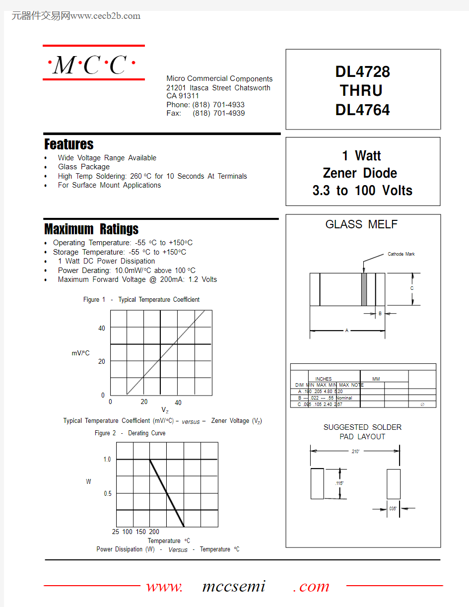
Figure 2 - Derating Curve
Power Dissipation (W) - Versus - Temperature °C
Temperature °C
W
0.5
1.0
Typical Temperature Coefficient (mV/°C) – versus – Zener Voltage (V Z)
Figure 1 - Typical Temperature Coefficient
02040
20
40
mV/°C
V Z
omp onents
21201 Itasca Street Chatsworth
! "#
$ % ! "#
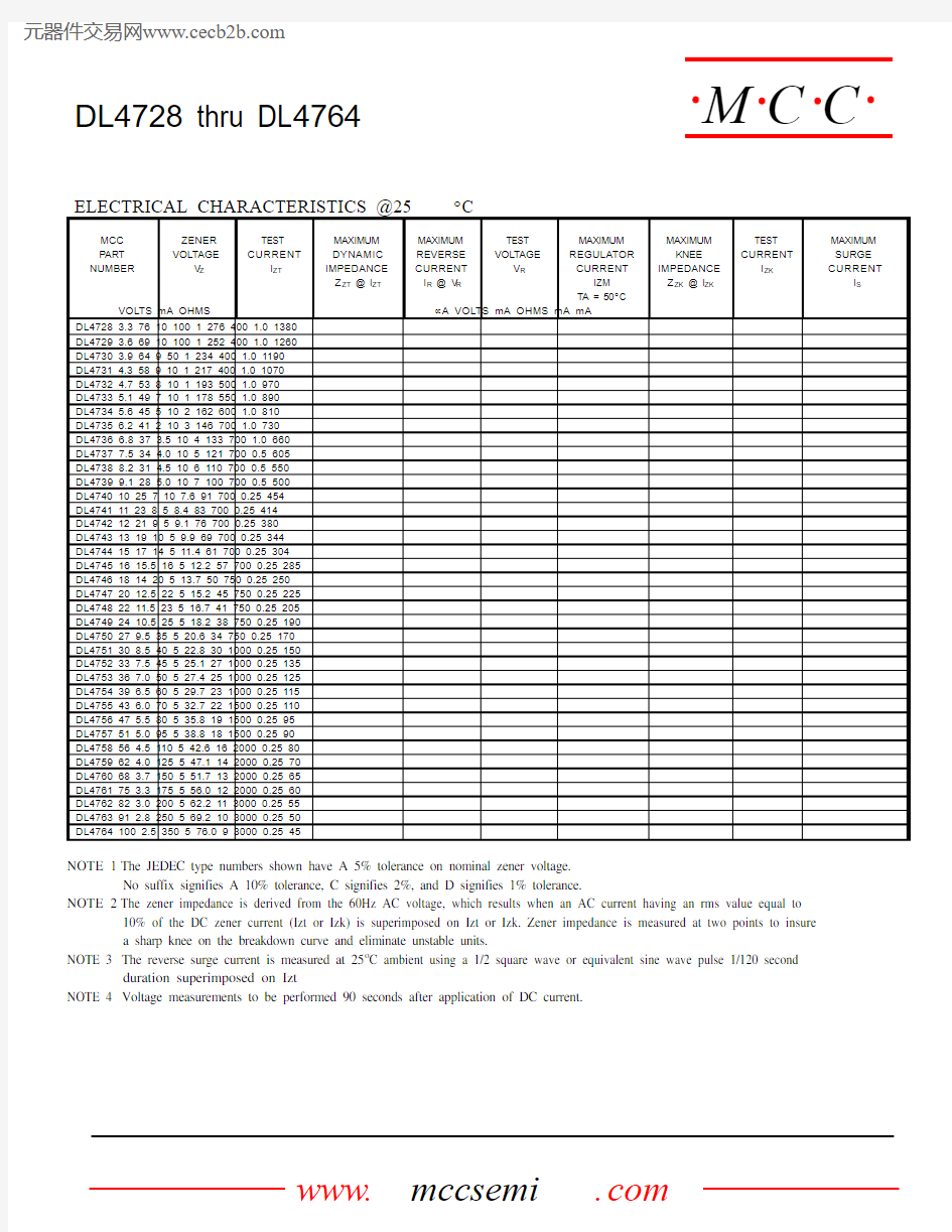
ELECTRICAL CHARACTERISTICS @25°C
MCC PART NUMBER
ZENER
VOLTAGE
V Z
TEST
CURRENT
I ZT
MAXIMUM
DYNAMIC
IMPEDANCE
Z ZT @ I ZT
MAXIMUM
REVERSE
CURRENT
I R @ V R
TEST
VOLTAGE
V R
MAXIMUM
REGULATOR
CURRENT
IZM
TA = 50°C
MAXIMUM
KNEE
IMPEDANCE
Z ZK @ I ZK
TEST
CURRENT
I ZK
MAXIMUM
SURGE
CURRENT
I S
VOLTS mA OHMS μA VOLTS mA OHMS mA mA DL4728 3.3 76 10 100 1 276 400 1.0 1380 DL4729 3.6 69 10 100 1 252 400 1.0 1260 DL4730 3.9 64 9 50 1 234 400 1.0 1190 DL4731 4.3 58 9 10 1 217 400 1.0 1070 DL4732 4.7 53 8 10 1 193 500 1.0 970 DL4733 5.1 49 7 10 1 178 550 1.0 890 DL4734 5.6 45 5 10 2 162 600 1.0 810 DL4735 6.2 41 2 10 3 146 700 1.0 730 DL4736 6.8 37 3.5 10 4 133 700 1.0 660 DL4737 7.5 34 4.0 10 5 121 700 0.5 605 DL4738 8.2 31 4.5 10 6 110 700 0.5 550 DL4739 9.1 28 5.0 10 7 100 700 0.5 500 DL4740 10 25 7 10 7.6 91 700 0.25 454 DL4741 11 23 8 5 8.4 83 700 0.25 414 DL4742 12 21 9 5 9.1 76 700 0.25 380 DL4743 13 19 10 5 9.9 69 700 0.25 344 DL4744 15 17 14 5 11.4 61 700 0.25 304 DL4745 16 15.5 16 5 12.2 57 700 0.25 285 DL4746 18 14 20 5 13.7 50 750 0.25 250 DL4747 20 12.5 22 5 15.2 45 750 0.25 225 DL4748 22 11.5 23 5 16.7 41 750 0.25 205 DL4749 24 10.5 25 5 18.2 38 750 0.25 190 DL4750 27 9.5 35 5 20.6 34 750 0.25 170 DL4751 30 8.5 40 5 22.8 30 1000 0.25 150 DL4752 33 7.5 45 5 25.1 27 1000 0.25 135 DL4753 36 7.0 50 5 27.4 25 1000 0.25 125 DL4754 39 6.5 60 5 29.7 23 1000 0.25 115 DL4755 43 6.0 70 5 32.7 22 1500 0.25 110 DL4756 47 5.5 80 5 35.8 19 1500 0.25 95 DL4757 51 5.0 95 5 38.8 18 1500 0.25 90 DL4758 56 4.5 110 5 42.6 16 2000 0.25 80 DL4759 62 4.0 125 5 47.1 14 2000 0.25 70 DL4760 68 3.7 150 5 51.7 13 2000 0.25 65 DL4761 75 3.3 175 5 56.0 12 2000 0.25 60 DL4762 82 3.0 200 5 62.2 11 3000 0.25 55 DL4763 91 2.8 250 5 69.2 10 3000 0.25 50 DL4764 100 2.5 350 5 76.0 9 3000 0.25 45
NOTE 1The JEDEC type numbers shown have A 5% tolerance on nominal zener voltage.
No suffix signifies A 10% tolerance, C signifies 2%, and D signifies 1% tolerance.
NOTE 2The zener impedance is derived from the 60Hz AC voltage, which results when an AC current having an rms value equal to 10% of the DC zener current (Izt or Izk) is superimposed on Izt or Izk. Zener impedance is measured at two points to insure
a sharp knee on the breakdown curve and eliminate unstable units.
NOTE 3 The reverse surge current is measured at 25o C ambient using a 1/2 square wave or equivalent sine wave pulse 1/120 second duration superimposed on Izt
NOTE 4 Voltage measurements to be performed 90 seconds after application of DC current.
DL4728 thru DL4764