
Universal Programmable Clock Generator
(UPCG)
CY22800
Features
?Spread Spectrum, VCXO, and Frequency Select ?Input frequency range:
—Crystal: 8–30 MHz
—CLKIN: 0.5–100 MHz
?Output frequency:
—LVCMOS: 1–200 MHz
?Integrated phase-locked loop
?Low jitter, high accuracy outputs
?3.3V operation
?8-pin SOIC package Benefits
?Make inventory of only one device, CY22800, to use in various applications such as HDTV, STB, DVDR, etc.?Multiple predefined configurations that can be programmed into a single chip
?Eliminates the need for expensive and difficult to use
higher-order crystal
?High-performance PLL tailored for multiple applications ?Meets critical timing requirements in complex system
designs
?Enables application compatibility
?Allows up to three different frequency selects
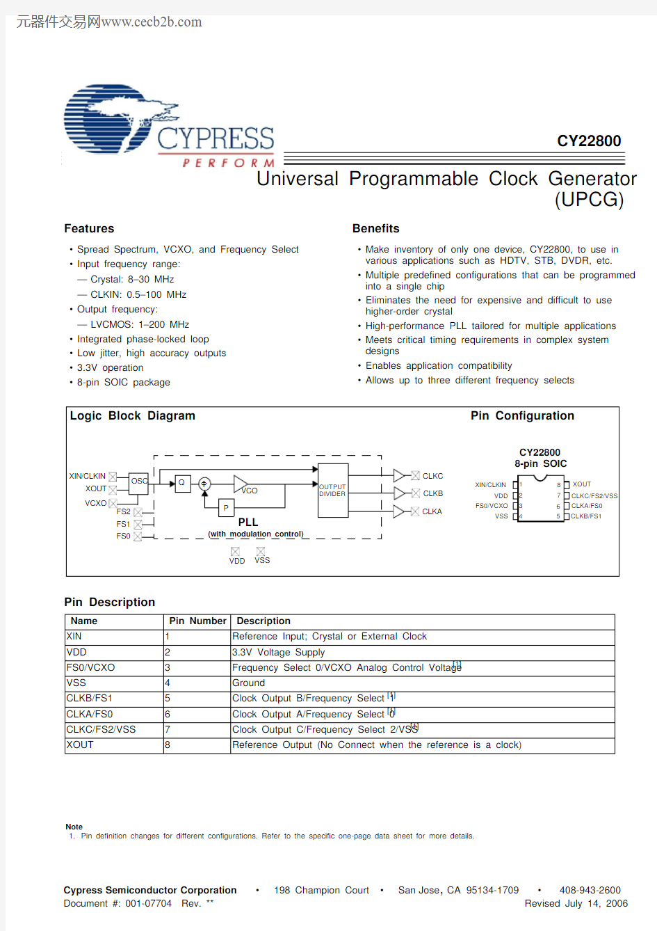
Pin Description
Name Pin Number Description
XIN1Reference Input; Crystal or External Clock
VDD2 3.3V Voltage Supply
FS0/VCXO3Frequency Select 0/VCXO Analog Control Voltage[1]
VSS4Ground
CLKB/FS15Clock Output B/Frequency Select 1[1]
CLKA/FS06Clock Output A/Frequency Select 0[1]
CLKC/FS2/VSS7Clock Output C/Frequency Select 2/VSS[1]
XOUT8Reference Output (No Connect when the reference is a clock) Note
1.Pin definition changes for different configurations. Refer to the specific one-page data sheet for more details.
CY22800
General Description
The CY22800 is a multi-function clock generator that supports various applications in consumer and communications markets. The device uses the Cypress proprietary PLL along with Spread Spectrum and VCXO technology to make it one of the most versatile clock synthesizer in the market place. The CY22800 is a field-programmable synthesizer that can be programmed using an easy-to-use programmer dongle, CY36800, with one of many predefined configuration files for fast sample generation of prototype builds. The CY22800 is a reprogrammable device that can be programmed up to five thousand times. The latest configurations available for this device are summarized in Table1.
Spread Spectrum Clock Generation (SSCG) The CY22800 is capable of generating Spread Spectrum Clocks (SSCG) for the purpose of reducing EMI found in today’s high-speed digital electronic systems.
The device uses proprietary Spread Spectrum Clock (SSC) technology to synthesize and modulate the frequency of the input clock. By modulating the frequency of the clock, the measured EMI at the fundamental and harmonic frequencies is greatly reduced. This reduction in radiated energy can significantly reduce the cost of complying with regulatory agency (EMC) requirements and improve time-to-market without degrading system performance.
The CY22800 uses a preprogrammed configuration of memory arrays to synthesize output frequency and offers eight different spread percentages (refer to Table1 – Code numbers -015 to -022), and an additional option to turn the spread on and off.
For the above-mentioned configurations, the modulation frequency varies with the reference frequency as follows:VCXO
One of the key components of the CY22800 device is the VCXO. The VCXO is used to “pull” the reference crystal higher or lower in order to lock the system frequency to an external source. This is ideal for applications where the output frequency needs to track along with an external reference frequency that is constantly shifting.
A special pullable crystal must be used in order to have adequate VCXO pull range. Pullable Crystal specifications are included in this data sheet.
VCXO Profile
Figure1 shows an example of what a VCXO profile looks like. The analog voltage input is on the X-axis and the PPM range is on the Y-axis. An increase in the VCXO input voltage results in a corresponding increase in the output frequency. This has the effect of moving the PPM from a negative to positive offset.
Figure 1. VCXO Profile
CY22800 Table 1.CY22800 Configurations
CY22800 Cypress offers a wide range of programmable clock synthesizers that can be used to generate any other frequencies not covered
by the CY22800. Table2 summarizes all Cypress programmable devices including CY22800.
Table 2.Cypress Programmable Clocks[2]
Part #No. of PLL Input Freq.Output
Freq.Package
No. of
Outputs
Spread
Spectrum VCXO I
2C
CY2280010.5–1001–2008-SOIC up to 3Yes Yes No CY2205011–1330.08–20016-TSSOP up to 6No No No CY2215011–1330.08–20016-TSSOP up to 6No No Yes CY2510018–1663–2008-SOIC/TSSOP up to 2Yes No No CY2520013–1663–20016-TSSOP up to 6Yes No No CY241V08127/13.527/13.58-SOIC up to 2No Yes No CY2239231–1661–20016-TSSOP up to 6No No No CY2238131–1661–2008-SOIC up to 3No No No CY2239331–1661–20016-TSSOP up to 6No No Yes CY22394/531–1661–20016-TSSOP up to 5No No No CY22388/89/9141–100 4.2–16616/20-TSSOP,
32-QFN
up to 8No Yes No
Note
2.The CY3672 programmer can be used to program all Cypress chips. Refer to the CY3672 data sheet for programming procedures.
CY22800
Absolute Maximum Conditions
Parameter Description Min.Max.Unit V DD Supply Voltage–0.5 4.6V T S Storage Temperature–65125°C T J Junction Temperature–125°C Digital Inputs V SS – 0.3V DD + 0.3V
Digital Outputs referred to V DD V SS – 0.3V DD + 0.3V
Electro-Static Discharge2–kV
Recommended Operating Conditions
Parameter Description Min.Typ.Max.Unit V DD Operating Voltage 3.14 3.3 3.47V T A Ambient Temperature0–70°C C LOAD Max. Load Capacitance on the CLK output––15pF f REF[3]Reference Frequency0.5–100MHz t PU Power-up time for all VDDs to reach minimum specified voltage (power ramps
0.05–500ms
must be monotonic)
Pullable Crystal Specifications for VCXO Application ONLY
Parameter Name Min.Typ.Max.Unit C LNOM Crystal Load Capacitance–14–pF R1Equivalent Series Resistance––25?
3–––R3/R1Ratio of Third Overtone Mode ESR to Fundamental Mode ESR. Ratio used
because typical R1 values are much less than the maximum spec
DL Crystal Drive Level. No external series resistor assumed–0.52mW F3SEPHI Third overtone separation from 3*F NOM (High Side)300––ppm F3SEPLO Third overtone separation from 3*F NOM (Low Side)–––150ppm C0Crystal shunt capacitance7pF C0/C1Ratio of Shunt to motional capacitance180–250
C1Crystal motional capacitance14.41821.6pF Recommended Crystal Specifications for ALL other Applications
Parameter Name Description Min.Typ.Max.Unit F NOM Nominal Crystal Frequency Parallel resonance, fundamental mode, and
8–30MHz
AT cut
C LNOM Nominal Load Capacitance–12–pF
Fundamental mode–3550?R1Equivalent Series Resistance
(ESR)
DL Crystal Drive Level No external series resistor assumed–0.52mW
Note
3.Configuration dependent, see the one-page document.
CY22800
Test Circuit
Figure 2. Test Circuit Diagram Figure 3. Duty Cycle Definition; DC = t2/t1
Figure 4. Rise and Fall Time Definitions
DC Electrical Specifications
Parameter Name
Description
Min.Typ.Max.Unit I OH Output High Current V OH = V DD – 0.5, V DD = 3.3V (source)1224–mA I OL Output Low Current V OL = 0.5, V DD = 3.3V (sink)1224–mA C IN1Input Capacitance All input pins except XIN and XOUT ––7pF C IN2Input Capacitance XIN and XOUT pins –24–pF I IH Input High Current V IH = V DD –510μA I IL Input Low Current V IL = 0V
––50
μA f ?XO VCXO Pullability Range ±150–ppm V VCXO VCXO Input Range 0–V DD V V IH Input High Voltage CMOS levels, 70% of V DD 0.7––V DD V IL
Input Low Voltage
CMOS levels, 30% of V DD
–
–
0.3V DD
AC Electrical Characteristics (V DD = 3.3V )
Parameter Name
Description
Min.Typ.Max.Unit DC Output Duty Cycle Duty Cycle is defined in Figure
3, 50% of V DD 455055%t 3Rising Edge Slew Rate Output Clock Rise Time, 20% - 80% of V DD 0.8 1.4–V/ns t 4Falling Edge Slew Rate Output Clock Fall Time, 80% - 20% of V DD
0.8 1.4–V/ns t 10
PLL Lock Time
–
–
3
ms
0.1μF
V DD
CLKout C LOAD
GND
OUTPUTS
CY22800
Document #: 001-07704 Rev. **Page 7 of 8
? Cypress Semiconductor Corporation, 2006. The information contained herein is subject to change without notice. Cypress Semiconductor Corporation assumes no responsibility for the use Package Diagram
Figure 5. 8-Lead (150-Mil) SOIC S8
All products and company names mentioned in this document may be the trademarks of their respective holders.
Ordering Information
Ordering Code Package Type Operating Range Operating Voltage CY22800FXC
8-Pin SOIC
Commercial
3.3V
51-85066-*C
CY22800
Document History Page
Document Title: CY22800 Universal Programmable Clock Generator
(UPCG)
Document Number: 001-07704
REV.ECN NO.Issue Date Orig. of
Change Description of Change **478688See ECN KKVTMP New data sheet