1 https://www.doczj.com/doc/5d12942790.html,/
2
https://www.doczj.com/doc/5d12942790.html,/
LTC1980
3
1980f
ELECTRICAL CHARACTERISTICS
SYMBOL PARAMETER
CONDITIONS MIN TYP MAX UNITS V RCHG2Recharge Threshold, Delta Voltage with Respect BATT 1 = Open 60
mV
to Float Voltage, Measured at OVP V LT0Charger Shorted Cell Threshold BATT2 = 0 2.55 2.7 2.8V V LT1Charger Shorted Cell Threshold
BATT2 = 1
5.2
5.4 5.65
V I BLDO Input Bias Current, Low Dropout Regulator Measured at LDOFB Pin
1.0μA g mldo Transconductance, Low Dropout Regulator Measured from LDOFB to LDODRV
350
μmhos
V OLLDO Output Low Voltage, Low Dropout Regulator 0.1
V V OHLDO Output High Voltage, Low Dropout Regulator V REG – 0.1
V I OUTLDO Low Dropout Regulator Output Current, Source/Sink ±20
μA A VOL Error Amplifier Open-Loop Voltage Gain From REGFB to V C
60
dB I BEA Error Amplifier Input Bias Current –0.10.1μA V OLEA Error Amplifier Output Low Voltage 0
0.5V V OHEA Error Amplifier Output High Voltage SS = Open
1.4
2
V I OUT Error Amplifier Output Source Current 0.5mA Error Amplifier Output Sink Current
–1.2
mA g mflt Float Voltage Error Amplifier Transconductance Measured from OVP to SS,65
μmhos
Charger Mode, BATT1 = Open
I BFLT Float Voltage Error Amplifier Input Current –0.10.1μA (Measured at OVP Input)V OS1Current Amplifier Offset Voltage –6
6
mV I BIS Input Bias Current, I SENSE Input –100
μA A VCA Current Amplifier Voltage Gain Measured from I SENSE to 2.3
2.44 2.55V/V CAOUT Pin
R PROG PROG Pin On Resistance 400?I PROG PROG Pin Leakage Current 100
nA f S Switching Frequency ●
260
300340kHz t r , t f Driver Output Transition Times C L = 15pF 10ns t BREAK Driver Output Break Times V BAT = V REG = 10V 100ns f TIMER Timer Frequency C = 1000pF
4.5kHz I TIMER1TIMER Pin Source Current –4μA I TIMER2TIMER Pin Sink Current 4μA R REG REG On Resistance 68?I REGPD REG Pull-Down Current 2
59μA I REGLK REG Leakage Current 60
nA V VTHREG REG Logic Threshold
0.3 1.3V V IL1Digital Input Low Voltage,
V REG = 5V 1.185 1.221 1.247V Negative-Going, Wall Adapter (WA)V IH1Digital Input High Voltage,
V REG = 5V
1.195
1.226 1.257V Positive-Going, Wall Adapter (WA)V IL2Digital Input Low Voltage, BATT1100mV V IH2
Digital Input High Voltage, BATT1
V BIAS2V
–100
The ● denotes the specifications which apply over the full operating
temperature range, otherwise specifications are at T A = 25°C. V BAT = 2.4V, V REG = 5V, V BAT unloaded.
https://www.doczj.com/doc/5d12942790.html,/
1980 G06
V BAT = 3.6V
100μs/DIV
V REG? 3.3V
I L = 100mA TO 500mA
T A = 25°C
FIGURE 5
4
https://www.doczj.com/doc/5d12942790.html,/
1μs/DIV V BAT = 3.6V
V REG = 3.3V
T A = 25°C
I L = 500mA 1980 G07
1μs/DIV
V BAT = 3.6V
V REG = 3.3V
I L = 500mA
T A = 25°C
FIGURE 5
1980 G081μs/DIV
V BAT = 3.6V
V REG? 3.3V
I L = 500mA
MODE = V BIAS1
T A = 25°C
1980 G09
200μs/DIV V BAT = 3.6V
V REG = 3.3V
I L = 10mA
T A = 25°C
FIGURE 51980 G10500μs/DIV
V BAT = 3.6V
V REG = 3.3V
V LDO = 3.1V
I LDO = 200mA
V WALL ADAPTER = 6V TO 0V
1980 G11
500μs/DIV
V BAT = 3.6V
V REG = 3.3V
V LDO = 3.1V
I LDO = 200mA
V WALL ADAPTER = 0V TO 6V
1980 G12
5ms/DIV
C TIMER = 0.24μF
T A = 25°C
1980 G14
https://www.doczj.com/doc/5d12942790.html,/
5
LTC1980
6
1980f
U U U
PI FU CTIO S
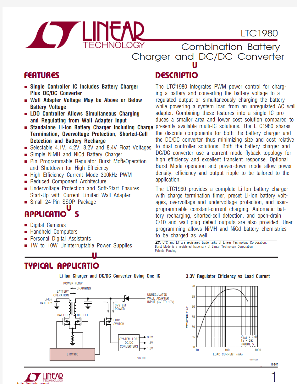
PROG (Pin 1): Charge Current Ratio Programming Pin.Programs the full charge current when the charger is in the constant current mode. A resistor placed between the PROG pin and the PROGT pin (Pin 2) determines the charge current. The PROG pin connects to an open drain MOSFET which turns on for full current and is off when trickle charging.
PROGT (Pin 2): Trickle Charge Programming Pin. Pro-grams the trickle charge current for a deeply discharged battery. Two resistors are used, one between the PROGT pin and CA OUT (Pin 22) and another from PROGT to ground. A capacitor between the PROGT pin and V C (Pin 4) provides compensation for the constant current feed-back loop.
REGFB (Pin 3): DC/DC Converter Feedback Pin. This pin is used to program the DC/DC converter output voltage when the LTC1980 is in the DC/DC (regulator) converter mode.An external resistor divider from V REG to REGFB to ground programs the output voltage. The virtual reference voltage (V REF ) on this pin is 1.225V. A series RC from the REGFB pin to V C (Pin 4) provides pole-zero compensation for the regulator outer loop.
V C (Pin 4): Control Signal of the Inner Loop of the Current Mode PWM. A common current mode loop is used by the battery charger and voltage regulator functions. Minimum duty factor (measured on BGTDR (Pin 14) in regulator mode and RGTDR (Pin 11) in charger mode) occurs at approximately 1V. Duty factor increases as V C increases.This part includes slope compensation, so there is some variation in V C for minimum and maximum duty factor as V REG or V BAT is varied.
LDO FB (Pin 5): Low Dropout Regulator F eedback Pin.This pin is used to program the low dropout linear regula-tor output voltage. An external resistor divider from the output of the LDO regulator (drain of the external MOSFET)to LDOFB to ground programs the output voltage. The virtual reference voltage on this pin is 1.225V.LDODRV (Pin 6): Low Dropout Error Amplifier Output.This pin drives the gate of an external PMOS pass transis-tor. This pin is pulled up to V REG (shutting off the pass transistor) if MODE (Pin 16) is grounded or if undervoltage occurs.
V REG (Pin 7): Connection Point to the DC/DC Converter Side of the Combo Charger/Converter Circuit.
WA (Pin 8): Wall Adapter Comparator Input. An external resistor divider from the wall adapter output to WA to ground sets the threshold which determines if charging can occur. If the wall adapter is below this threshold, the LTC1980 assumes the wall adapter is not present and the charger shuts down. Wall adapter sense threshold is set higher than the DC/DC converter output voltage to insure correct operation.
BATT1 (Pin 9): Logic Input Pin for Selecting Preprogrammed Li-Ion Charge Voltage. See Truth Table logic settings.
BATT2 (Pin 10): Logic Input Pin for Selecting Preprogrammed Li-Ion Charge Voltage. The following combinations of BATT1 and BATT2 select the correct Li-Ion charge voltage. See Truth Table.
BATT2BATT1FLOAT VOLTAGE
00 4.1V 01 4.2V 108.2V 118.4V
Don’t Care
Open
Externally Set Via OVP
Logic 1 = V BIAS2 (Pin 19), Logic 0 = GND
RGTDR (Pin 11): DC/DC Converter (Regulator) Side Gate Drive Pin. This pin provides gate drive to the external MOSFET (REG-FET) that connects to V REG via the trans-former.
PGND (Pin 12): Power Ground. Refer to the Applications Information section for proper use of ground and power ground connections.
V BIAS1 (Pin 13): Internally Generated Power Bus. Bypass this pin with a 1μF or larger ceramic capacitor (or other low ESR capacitor) to PGND (Pin 12). Do not connect any load to this pin.
BGTDR (Pin 14): DC/DC Converter (Battery) Side Gate Drive Pin. This pin provides gate drive to the external MOSFET (BAT-FET) that connects to V BAT via the trans-former.
https://www.doczj.com/doc/5d12942790.html,/
LTC1980
7
1980f
REG (Pin 15): Bidirectional Regulator Mode Control Pin. A pull-up resistor is required between this pin and V BIAS2.This pin is open when charging normally, has a weak pull-down (approximately 5μA) when conditioning the battery and a strong pull-down when in regulator mode. Pulling this pin low forces the IC into regulator mode.MODE (Pin 16): Selects different operating modes in both charger and DC/DC converter configurations. Also en-ables and disables Burst Mode operation. See Mode Pin Operation table in Application section.
TIMER (Pin 17): A timing capacitor on this pin determines the normal charge time for charge termination.C(μF) = 0.25 ? Time (Hours)
V BAT (Pin 18): This pin connects to the positive terminal of the battery and the battery side of the power converter.V BIAS2 (Pin 19): Internally Generated Voltage. Bypass this pin with a 1μF or larger ceramic capacitor (or other low ESR capacitor). Do not connect any load to this pin.GND (Pin 20): Signal Ground. This pin should Kelvin-connect to the current sense resistor (R SENSE ).
I SENSE (Pin 21): Current Sense Input Pin. Connects inter-nally to a current amplifier and zero current comparator.This pin should Kelvin-connect to the current sense resis-tor (R SENSE ) .
CAO UT (Pin 22): Current Amplifier Output. A program resistor connects between this pin and PROGT (Pin 2) to set the charge current (in constant-current mode).OVP (Pin 23): Overvoltage Protection. This pin connects to the tap on an optional external voltage divider con-nected across the battery. This allows nonstandard float voltages to be used for the battery charger. Overvoltage,restart and undervoltage thresholds will also be affected by the external voltage division ratio. To use this pin,BATT1 (Pin 9) must float.
SS (Pin 24): Soft-Start. A capacitor between this pin and ground sets the battery charge ramp rate. Battery charge current is very low the moment after the converter switches from DC/DC converter (regulator) mode to battery charger mode then ramps up to final battery charge current from there. This insures that the wall adapter is not loaded down with a large inrush current that could prevent correct battery charger operation.
The same capacitor, which sets the soft-start ramp rate,also sets the compensation for the battery float voltage control loop.
U U U
PI FU CTIO S
https://www.doczj.com/doc/5d12942790.html,/
8
https://www.doczj.com/doc/5d12942790.html,/
9 https://www.doczj.com/doc/5d12942790.html,/
10 https://www.doczj.com/doc/5d12942790.html,/
分销商库存信息:
LINEAR-TECHNOLOGY
LTC1980EGN#PBF LTC1980EGN LTC1980EGN#TR LTC1980EGN#TRPBF