
S T E L L A R I S E R R A T A
Stellaris ?
LM3S1512RevA2Errata
This document contains known errata at the time of publication for the Stellaris LM3S1512
microcontroller.The table below summarizes the errata and lists the affected revisions.See the data sheet for more details.
See also the ARM?Cortex?-M3errata,ARM publication number PR326-PRDC-009450v2.0.
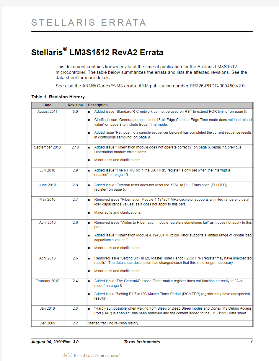
Table 1.Revision History
Description Revision Date ■Added issue “Standard R-C network cannot be used on RST to extend POR timing”on page 5.■Clarified issue “General-purpose timer 16-bit Edge Count or Edge Time mode does not load reload value”on page 8to include Edge-Time mode.
■
Added issue “Retriggering a sample sequencer before it has completed the current sequence results in continuous sampling”on page 9.
3.0
August 2011
■Added issue “Hibernation module does not operate correctly”on page 6,replacing previous Hibernation module errata items.■
Minor edits and clarifications.
2.10September 2010■
Added issue “The RTRIS bit in the UARTRIS register is only set when the interrupt is enabled”on page 10.
2.9July 2010■
Added issue “External reset does not reset the XTAL to PLL Translation (PLLCFG)register”on page 5.
2.8June 2010■Removed issue "Hibernation Module 4.194304-MHz oscillator supports a limited range of crystal load capacitance values"as it does not apply to this part.■
Minor edits and clarifications.
2.7May 2010■Removed issue "Writes to Hibernation module registers sometimes fail"as it does not apply to this part.
■Added issue "Hibernation Module 4.194304-MHz oscillator supports a limited range of crystal load capacitance values."■
Minor edits and clarifications.
2.6April 2010■Removed issue "Setting Bit 7in I2C Master Timer Period (I2CMTPR)register may have unexpected results".The data sheet description has changed such that this is no longer necessary.■
Minor edits and clarifications.
2.5April 2010■Added issue “The General-Purpose Timer match register does not function correctly in 32-bit mode”on page 8.
■
Added issue "Setting Bit 7in I2C Master Timer Period (I2CMTPR)register may have unexpected results".
2.4February 2010■
"Hard Fault possible when waking from Sleep or Deep-Sleep modes and Cortex-M3Debug Access Port (DAP)is enabled"has been removed and the content added to the LM3S1512data sheet.
2.3Jan 2010Started tracking revision history.
2.2Dec 20091
Texas Instruments August 04,2011/Rev.3.0
Stellaris LM3S1512A2Errata
Table2.List of Errata
2
August04,2011/Rev.3.0
Texas Instruments
Stellaris LM3S1512A2Errata
1JTAG and Serial Wire Debug
1.1JTAG pins do not have internal pull-ups enabled at power-on reset
Description:
Following a power-on reset,the JTAG pins TRST,TCK,TMS,TDI,and TDO(PB7and PC[3:0])do
not have internal pull-ups enabled.Consequently,if these pins are not driven from the board,two
things may happen:
■The JTAG port may be held in reset and communication with a four-pin JTAG-based debugger may be intermittent or impossible.
■The receivers may draw excess current.
Workaround:
There are a number of workarounds for this problem,varying in complexity and impact:
1.Add external pull-up resistors to all of the affected pins.This workaround solves both issues of
JTAG connectivity and current consumption.
2.Add an external pull-up resistor to TRST.Firmware should enable the internal pull-ups on the
affected pins by setting the appropriate PUE bits of the appropriate GPIO Pull-Up Select
(GPIOPUR)registers as early in the reset handler as possible.This workaround addresses the
issue of JTAG connectivity,but does not address the current consumption other than to limit
the affected period(from power-on reset to code execution).
3.Pull-ups on the JTAG pins are unnecessary for code loaded via the SWD interface or via the
serial boot loader.Loaded firmware should enable the internal pull-ups on the affected pins by
setting the appropriate PUE bits of the appropriate GPIOPUR registers as early in the reset
handler as possible.This method does not address the current consumption other than to limit
the affected period(from power-on reset to code execution).
Silicon Revision Affected:
A2
1.2JTAG INTEST instruction does not work
Description:
The JTAG INTEST(Boundary Scan)instruction does not properly capture data.
Workaround:
None.
Silicon Revision Affected:
A2
August04,2011/Rev.3.0
3
Texas Instruments
Stellaris LM3S1512A2Errata
2System Control
2.1Clock source incorrect when waking up from Deep-Sleep mode in
some configurations
Description:
In some clocking configurations,the core prematurely starts executing code before the main oscillator
(MOSC)has stabilized after waking up from Deep-Sleep mode.This situation can cause undesirable
behavior for operations that are frequency dependent,such as UART communication.
This issue occurs if the system is configured to run off the main oscillator,with the PLL bypassed
and the DSOSCSRC field of the Deep-Sleep Clock Configuration(DSLPCLKCFG)register set to
use the internal12-MHz oscillator,30-KHz internal oscillator,or32-KHz external oscillator.When
the system is triggered to wake up,the core should wait for the main oscillator to stabilize before
starting to execute code.Instead,the core starts executing code while being clocked from the
deep-sleep clock source set in the DSLPCLKCFG register.When the main oscillator stabilizes,the
clock to the core is properly switched to run from the main oscillator.
Workaround:
Run the system off of the main oscillator(MOSC)with the PLL enabled.In this mode,the clocks
are switched at the proper time.
If the main oscillator must be used to clock the system without the PLL,a simple wait loop at the
beginning of the interrupt handler for the wake-up event should be used to stall the
frequency-dependent operation until the main oscillator has stabilized.
Silicon Revision Affected:
A2
2.2PLL may not function properly at default LDO setting
Description:
In designs that enable and use the PLL module,unstable device behavior may occur with the LDO
set at its default of2.5volts or below(minimum of2.25volts).Designs that do not use the PLL
module are not affected.
Workaround:
Prior to enabling the PLL module,it is recommended that the default LDO voltage setting of2.5V
be adjusted to2.75V using the LDO Power Control(LDOPCTL)register.
Silicon Revision Affected:
A2
2.3I/O buffer5-V tolerance issue
Description:
GPIO buffers are not5-V tolerant when used in open-drain mode.Pulling up the open-drain pin
above4V results in high current draw.
August04,2011/Rev.3.0 4
Texas Instruments
Stellaris LM3S1512A2Errata
Workaround:
When configuring a pin as open drain,limit any pull-up resistor connections to the3.3-V power rail.
Silicon Revision Affected:
A2
2.4PLL Runs Fast When Using a
3.6864-MHz Crystal
Description:
If the PLL is enabled,and a3.6864-MHz crystal is used,the PLL runs4%fast.
Workaround:
Use a different crystal whose frequency is one of the other allowed crystal frequencies(see the
values shown for the XTAL bit in the RCC register).
Silicon Revision Affected:
A2
2.5External reset does not reset the XTAL to PLL Translation(PLLCFG)
register
Description:
Performing an external reset(anything but power-on reset)reconfigures the XTAL field in the
Run-Mode Clock Configuration(RCC)register to the6MHz setting,but does not reset the XTAL
to PLL Translation(PLLCFG)register to the6MHz setting.
Consider the following sequence:
1.Performing a power-on reset results in XTAL=6MHz and PLLCFG=6MHz
2.Write an8MHz value to the XTAL field results in XTAL=8MHz and PLLCFG=8MHz
3.RST asserted results in XTAL=6MHz and PLLCFG=8MHz
In the last step,PLLCFG was not reset to its6MHz setting.If this step is followed by enabling the
PLL to run from an attached6-MHz crystal,the PLL then operates at300MHz instead of400MHz.
Subsequently configuring the XTAL field with the8MHz setting does not change the setting of
PLLCFG.
Workaround:
Set XTAL in PLLCFG to an incorrect value,and then to the desired value.The second change
updates the register correctly.Do not enable the PLL until after the second change.
Silicon Revision Affected:
A2
2.6Standard R-C network cannot be used on RST to extend POR timing
Description:
The standard R-C network on RST does not work to extend POR timing beyond the10ms on-chip
POR.Instead of following the standard capacitor charging curve,RST jumps straight to3V at power
5 August04,2011/Rev.3.0
Texas Instruments
Stellaris LM3S1512A2Errata
on.The capacitor is fully charged by current out of the RST pin and does not extend or filter the
power-on condition.As a result,the reset input is not extended beyond the POR.
Workaround:
Add a diode to block the output current from RST.This helps to extend the RST pulse,but also
means that the R-C is not as effective as a noise filter.
Silicon Revision Affected:
A2
3Hibernation Module
3.1Hibernation module does not operate correctly
Description:
The Hibernation module on this microcontroller does not operate correctly.
Workaround:
This errata item does not apply to many Stellaris devices,including the LM3S1166,LM3S1636,
LM3S1969,and LM3S2919.Refer to the Stellaris Product Selector Guide
(https://www.doczj.com/doc/6a11743072.html,/stellaris_search)and Errata documents to find an alternative microcontroller that meets
the design requirements for your application.
Silicon Revision Affected:
A2
4GPIO
4.1GPIO input pin latches in the Low state if pad type is open drain
Description:
GPIO pins function normally if configured as inputs and the open-drain configuration is disabled.If
open drain is enabled while the pin is configured as an input using the GPIO Alternate Function
Select(GPIOAFSEL),GPIO Open Drain Select(GPIOODR),and GPIO Direction(GPIODIR)
registers,then the pin latches Low and excessive current(into pin)results if an attempt is made to
drive the pin High.The open-drain device is not controllable.
A GPIO pin is not normally configured as open drain and as an input at the same time.A user may
want to do this when driving a signal out of a GPIO open-drain pad while configuring the pad as an
input to read data on the same pin being driven by an external device.Bit-banging a bidirectional,
open-drain bus(for example,I2C)is an example.
Workaround:
If a user wants to read the state of a GPIO pin on a bidirectional bus that is configured as an
open-drain output,the user must first disable the open-drain configuration and then change the
direction of the pin to an input.This precaution ensures that the pin is never configured as an input
and open drain at the same time.
A second workaround is to use two GPIO pins connected to the same bus signal.The first GPIO
pin is configured as an open-drain output,and the second is configured as a standard input.This
August04,2011/Rev.3.0 6
Texas Instruments
Stellaris LM3S1512A2Errata way the open-drain output can control the state of the signal and the input pin allows the user to
read the state of the signal without causing the latch-up condition.
Silicon Revision Affected:
A2
4.2GPIO pins may glitch during power supply ramp up
Description:
Upon completing a POR(power on reset)sequence,the GPIO pins default to a tri-stated input
condition.However,during the initial ramp up of the external V DD supply from0.0V to3.3V,the
GPIO pins are momentarily configured as output drivers during the time the internal LDO circuit is
also ramping up.As a result,a signal glitch may occur on GPIO pins before both the external V DD
supply and internal LDO voltages reach their normal operating conditions.This situation can occur
when the V DD and LDO voltages ramp up at significantly different rates.The LDO voltage ramp-up
time is affected by the load capacitance on the LDO pin,therefore,it is important to keep this load
at a nominal1μF value as recommended in the data sheet.Adding significant more capacitance
loading beyond the specification causes the time delay between the two supply ramp-up times to
grow,which possibly increases the severity of the glitching behavior.
Workaround:
Ensuring that the V DD power supply ramp up is a fast as possible helps minimize the potential for
GPIO glitches.Follow guidelines for LDO pin capacitive loading documented in the electrical section
of the data sheet.System designers must ensure that,during the V DD supply ramp-up time,possible
GPIO pin glitches can cause no adverse effects to their systems.
Silicon Revision Affected:
A2
5General-Purpose Timers
5.1General-purpose timer Edge Count mode count error when timer
is disabled
Description:
When a general-purpose timer is configured for16-Bit Input Edge Count Mode,the timer(A or B)
erroneously decrements by one when the Timer Enable(TnEN)bit in the GPTM Control
(GPTMCTL)register is cleared(the timer is disabled).
Workaround:
When the general-purpose timer is configured for Edge Count mode and software needs to“stop”
the timer,the timer should be reloaded with the current count+1and restarted.
Silicon Revision Affected:
A2
7 August04,2011/Rev.3.0
Texas Instruments
Stellaris LM3S1512A2Errata
5.2General-purpose timer16-bit Edge Count or Edge Time mode does
not load reload value
Description:
In Edge Count or Edge Time mode,the input events on the CCP pin decrement the counter until the
count matches what is in the GPTM Timern Match(GPTMTnMATCHR)register.At that point,an
interrupt is asserted and then the counter should be reloaded with the original value and counting
begins again.However,the reload value is not reloaded into the timer.
Workaround:
Rewrite the GPTM Timern Interval Load(GPTMTnILR)register before restarting.
Silicon Revision Affected:
A2
5.3The General-Purpose Timer match register does not function
correctly in32-bit mode
Description:
The GPTM Timer A Match(GPTMTAMATCHR)register triggers a match interrupt when the lower
16bits match,regardless of the value of the upper16bits.
Workaround:
None.
Silicon Revision Affected:
A2
6ADC
6.1Use of"Always"triggering for ADC Sample Sequencer3does not
work
Description:
When using ADC Sample Sequencer3(SS3)and configuring the trigger source to"Always"to
enable continuous sampling by programming the SS3Trigger Select field(EM3)in the ADC Event
Multiplexer Select(ADCEMUX)register to0xF,the first sample will be captured,but no further
samples will be updated to the sequencer FIFO.Interrupts are continuously generated after the first
sample and the FIFO status remains empty.
Workaround:
Software must disable and re-enable the sample sequencer to capture another sample.
Silicon Revision Affected:
A2
8
August04,2011/Rev.3.0
Texas Instruments
Stellaris LM3S1512A2Errata 6.2Incorrect behavior with timer ADC triggering when another timer
is used in32-bit mode
Description:
When a timer is configured to trigger the ADC and another timer is configured to be a32-bit periodic
or one-shot timer,the ADC is triggered continuously instead of the specified interval.
Workaround:
Do not use a32-bit periodic or one-shot timer when triggering ADC.If the timer is in16-bit mode,
the ADC trigger works as expected.
Silicon Revision Affected:
A2
6.3ADC hardware averaging produces erroneous results in differential
mode
Description:
The implementation of the ADC averaging circuit does not work correctly when the ADC is sampling
in differential mode and the difference between the voltages is approximately0.0V.
Workaround:
Do not use hardware averaging in differential mode.Instead,use the FIFO to store results and
average them in software.
Silicon Revision Affected:
A2
6.4Retriggering a sample sequencer before it has completed the
current sequence results in continuous sampling
Description:
Re-triggering a sample sequencer before it has completed its programmed conversion sequence
causes the sample sequencer to continuously sample.If interrupts have been enabled,interrupts
are generated at the appropriate place in the sample sequence.This problem only occurs when the
new trigger is the same type as the current trigger.
Workaround:
Ensure that a sample sequence has completed before triggering a new sequence using the same
type of trigger.
Silicon Revision Affected:
A2
August04,2011/Rev.3.0
9
Texas Instruments
7
UART
7.1
The RTRIS bit in the UARTRIS register is only set when the interrupt is enabled
Description:
The RTRIS (UART Receive Time-Out Raw Interrupt Status)bit in the UART Raw Interrupt Status (UARTRIS)register should be set when a receive time-out occurs,regardless of the state of the enable RTIM bit in the UART Interrupt Mask (UARTIM)register.However,currently the RTIM bit must be set in order for the RTRIS bit to be set when a receive time-out occurs.Workaround:
For applications that require polled operation,the RTIM bit can be set while the UART interrupt is disabled in the NVIC using the IntDisable(n)function in the StellarisWare Peripheral Driver Library,where n is 21,22,or 49depending whether UART0,UART1or UART2is used.With this configuration,software can poll the RTRIS bit,but the interrupt is not reported to the NVIC.Silicon Revision Affected:A2
8
QEI
8.1
QEI index resets position when index is disabled
Description:
When the QEI module is configured to not reset the position on detection of the index signal (that is,the ResMode bit in the QEI Control (QEICTL)register is 0),the module resets the position when the index pulse occurs.The position counter should only be reset when it reaches the maximum value set in the QEI Maximum Position (QEIMAXPOS)register.Workaround:
Do not rely on software to disable the index pulse.Do not connect the index pulse if it is not needed.Silicon Revision Affected:A2
8.2QEI hardware position can be wrong under certain conditions
Description:
The QEI Position (QEIPOS)register can be incorrect if the QEI is configured for quadrature phase mode (SigMode bit in QEICTL register =0)and to update the position counter of every edge of both PhA and PhB (CapMode bit in QEICTL register =1).This error can occur if the encoder is stepped in the reverse direction,stepped forward once,and then continues in the reverse direction.The following sequence of transitions on the PhA and PhB pins causes the error:
PhB
August 04,2011/Rev.3.0
Texas Instruments
10Stellaris LM3S1512A2Errata
Assuming the starting position prior to the above PhA and PhB sequence is0,the position after the
falling edge on PhB should be-3,however the QEIPOS register will show the position to be-1.
Workaround:
Configure the QEI to update the position counter on every edge on PhA only(CapMode bit in QEICTL
register=0).The effective resolution is reduced by50%.If full resolution position detection is required
by updating the position counter on every edge of both PhA and PhB,no workaround is available.
Hardware and software must take this into account.
Silicon Revision Affected:
A2
Copyright?2007-2011Texas Instruments Incorporated All rights reserved.Stellaris and StellarisWare are registered trademarks of Texas Instruments Incorporated.ARM and Thumb are registered trademarks and Cortex is a trademark of ARM Limited.Other names and brands may be claimed as the property of others.
Texas Instruments Incorporated
108Wild Basin,Suite350
Austin,TX78746
https://www.doczj.com/doc/6a11743072.html,/stellaris
https://www.doczj.com/doc/6a11743072.html,/sc/technical-support/product-information-centers.htm
11 August04,2011/Rev.3.0
Texas Instruments
IMPORTANT NOTICE
Texas Instruments Incorporated and its subsidiaries(TI)reserve the right to make corrections,modifications,enhancements,improvements, and other changes to its products and services at any time and to discontinue any product or service without notice.Customers should obtain the latest relevant information before placing orders and should verify that such information is current and complete.All products are sold subject to TI’s terms and conditions of sale supplied at the time of order acknowledgment.
TI warrants performance of its hardware products to the specifications applicable at the time of sale in accordance with TI’s standard warranty.Testing and other quality control techniques are used to the extent TI deems necessary to support this warranty.Except where mandated by government requirements,testing of all parameters of each product is not necessarily performed.
TI assumes no liability for applications assistance or customer product design.Customers are responsible for their products and applications using TI components.To minimize the risks associated with customer products and applications,customers should provide adequate design and operating safeguards.
TI does not warrant or represent that any license,either express or implied,is granted under any TI patent right,copyright,mask work right, or other TI intellectual property right relating to any combination,machine,or process in which TI products or services are https://www.doczj.com/doc/6a11743072.html,rmation published by TI regarding third-party products or services does not constitute a license from TI to use such products or services or a warranty or endorsement https://www.doczj.com/doc/6a11743072.html,e of such information may require a license from a third party under the patents or other intellectual property of the third party,or a license from TI under the patents or other intellectual property of TI.
Reproduction of TI information in TI data books or data sheets is permissible only if reproduction is without alteration and is accompanied by all associated warranties,conditions,limitations,and notices.Reproduction of this information with alteration is an unfair and deceptive business practice.TI is not responsible or liable for such altered https://www.doczj.com/doc/6a11743072.html,rmation of third parties may be subject to additional restrictions.
Resale of TI products or services with statements different from or beyond the parameters stated by TI for that product or service voids all express and any implied warranties for the associated TI product or service and is an unfair and deceptive business practice.TI is not responsible or liable for any such statements.
TI products are not authorized for use in safety-critical applications(such as life support)where a failure of the TI product would reasonably be expected to cause severe personal injury or death,unless officers of the parties have executed an agreement specifically governing such use.Buyers represent that they have all necessary expertise in the safety and regulatory ramifications of their applications,and acknowledge and agree that they are solely responsible for all legal,regulatory and safety-related requirements concerning their products and any use of TI products in such safety-critical applications,notwithstanding any applications-related information or support that may be provided by TI.Further,Buyers must fully indemnify TI and its representatives against any damages arising out of the use of TI products in such safety-critical applications.
TI products are neither designed nor intended for use in military/aerospace applications or environments unless the TI products are specifically designated by TI as military-grade or"enhanced plastic."Only products designated by TI as military-grade meet military specifications.Buyers acknowledge and agree that any such use of TI products which TI has not designated as military-grade is solely at the Buyer's risk,and that they are solely responsible for compliance with all legal and regulatory requirements in connection with such use. TI products are neither designed nor intended for use in automotive applications or environments unless the specific TI products are designated by TI as compliant with ISO/TS16949requirements.Buyers acknowledge and agree that,if they use any non-designated products in automotive applications,TI will not be responsible for any failure to meet such requirements.
Following are URLs where you can obtain information on other Texas Instruments products and application solutions:
Products Applications
Audio https://www.doczj.com/doc/6a11743072.html,/audio Communications and Telecom https://www.doczj.com/doc/6a11743072.html,/communications
Amplifiers https://www.doczj.com/doc/6a11743072.html, Computers and Peripherals https://www.doczj.com/doc/6a11743072.html,/computers
Data Converters https://www.doczj.com/doc/6a11743072.html, Consumer Electronics https://www.doczj.com/doc/6a11743072.html,/consumer-apps
DLP?Products https://www.doczj.com/doc/6a11743072.html, Energy and Lighting https://www.doczj.com/doc/6a11743072.html,/energy
DSP https://www.doczj.com/doc/6a11743072.html, Industrial https://www.doczj.com/doc/6a11743072.html,/industrial
Clocks and Timers https://www.doczj.com/doc/6a11743072.html,/clocks Medical https://www.doczj.com/doc/6a11743072.html,/medical
Interface https://www.doczj.com/doc/6a11743072.html, Security https://www.doczj.com/doc/6a11743072.html,/security
Logic https://www.doczj.com/doc/6a11743072.html, Space,Avionics and Defense https://www.doczj.com/doc/6a11743072.html,/space-avionics-defense Power Mgmt https://www.doczj.com/doc/6a11743072.html, Transportation and Automotive https://www.doczj.com/doc/6a11743072.html,/automotive
Microcontrollers https://www.doczj.com/doc/6a11743072.html, Video and Imaging https://www.doczj.com/doc/6a11743072.html,/video
RFID https://www.doczj.com/doc/6a11743072.html,
OMAP Mobile Processors https://www.doczj.com/doc/6a11743072.html,/omap
Wireless Connctivity https://www.doczj.com/doc/6a11743072.html,/wirelessconnectivity
TI E2E Community Home Page https://www.doczj.com/doc/6a11743072.html,
Mailing Address:Texas Instruments,Post Office Box655303,Dallas,Texas75265
Copyright?2011,Texas Instruments Incorporated