FEATURES
DESCRIPTION
APPLICATIONS
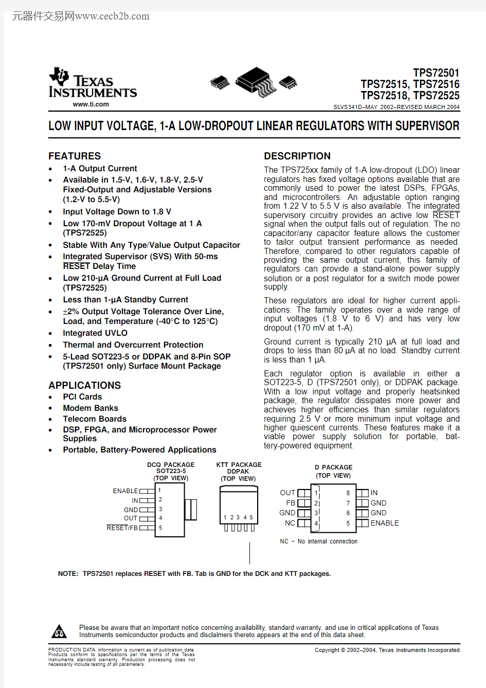
12345
DCQ PACKAGE RESET/FB
OUT GND IN ENABLE SOT223-5(TOP VIEW)
1234
8765
OUT FB GND NC
IN GND GND ENABLE
D PACKAG
E (TOP VIEW)
NC ? No internal connection
1KTT PACKAGE
(TOP VIEW)
2345
E N A B L E I N G N D O U T DDPAK R E S E T /
F B
TPS72501
TPS72515,TPS72516TPS72518,TPS72525
SLVS341D–MAY 2002–REVISED MARCH 2004
LOW INPUT VOLTAGE,1-A LOW-DROPOUT LINEAR REGULATORS WITH SUPERVISOR
?1-A Output Current
The TPS725xx family of 1-A low-dropout (LDO)linear regulators has fixed voltage options available that are ?
Available in 1.5-V,1.6-V,1.8-V,2.5-V commonly used to power the latest DSPs,FPGAs,Fixed-Output and Adjustable Versions and microcontrollers.An adjustable option ranging (1.2-V to 5.5-V)
from 1.22V to 5.5V is also available.The integrated ?Input Voltage Down to 1.8V
supervisory circuitry provides an active low RESET ?Low 170-mV Dropout Voltage at 1A signal when the output falls out of regulation.The no (TPS72525)
capacitor/any capacitor feature allows the customer to tailor output transient performance as needed.?Stable With Any Type/Value Output Capacitor Therefore,compared to other regulators capable of ?Integrated Supervisor (SVS)With 50-ms providing the same output current,this family of RESET Delay Time
regulators can provide a stand-alone power supply ?Low 210-μA Ground Current at Full Load solution or a post regulator for a switch mode power supply.
(TPS72525)
?Less than 1-μA Standby Current
These regulators are ideal for higher current appli-cations.The family operates over a wide range of ?±2%Output Voltage Tolerance Over Line,input voltages (1.8V to 6V)and has very low Load,and Temperature (-40°C to 125°C)dropout (170mV at 1-A).
?Integrated UVLO
Ground current is typically 210μA at full load and ?Thermal and Overcurrent Protection
drops to less than 80μA at no load.Standby current ?
5-Lead SOT223-5or DDPAK and 8-Pin SOP is less than 1μA.
(TPS72501only)Surface Mount Package
Each regulator option is available in either a SOT223-5,D (TPS72501only),or DDPAK package.With a low input voltage and properly heatsinked ?PCI Cards package,the regulator dissipates more power and ?Modem Banks achieves higher efficiencies than similar regulators ?Telecom Boards
requiring 2.5V or more minimum input voltage and higher quiescent currents.These features make it a ?DSP,FPGA,and Microprocessor Power viable power supply solution for portable,bat-Supplies
tery-powered equipment.
?
Portable,Battery-Powered Applications
NOTE:TPS72501replaces RESET with FB.Tab is GND for the DCK and KTT packages.
Please be aware that an important notice concerning availability,standard warranty,and use in critical applications of Texas Instruments semiconductor products and disclaimers thereto appears at the end of this data sheet.
https://www.doczj.com/doc/7719060844.html,
These devices have limited built-in ESD protection.The leads should be shorted together or the device placed in conductive foam during storage or handling to prevent electrostatic damage to the MOS gates.
Although an output capacitor is not required for stability,transient response and output noise are improved with a 10-μF output capacitor.
Unlike some regulators that have a minimum current requirement,the TPS725family is stable with no output load current.The low noise capability of this family,coupled with its high current operation and ease of power dissipation,make it ideal for telecom boards,modem banks,and other noise-sensitive applications.
ORDERING INFORMATION
(1)Other voltage options are available upon request from the manufacturer.
(2)To order a taped and reeled part,add the suffix R to the part number(e.g.,TPS72501DCQ R).
(3)To order a50-piece reel,add the suffix T(e.g.,TPS72501KTT T);to order a500-piece reel,add the suffix R(e.g.,TPS72501KTT R).
(4)To order a taped and reeled part,add the suffix R or T(2500or500)to the part number(e.g.TPS72501D R)
over operating free-air temperature range unless otherwise noted(1)
(1)Stresses beyond those listed under absolute maximum ratings may cause permanent damage to the device.These are stress ratings
only,and functional operation of the device at these or any other conditions beyond those indicated under recommended operating conditions is not implied.Exposure to absolute-maximum-rated conditions for extended periods may affect device reliability.
(2)All voltage values are with respect to network ground terminal.
(1)Minimum V I=V O(nom)+V DO.
https://www.doczj.com/doc/7719060844.html,
Line regulation(mV)+ǒ%ńVǔV Oǒ5.5V)V Iminǔ
100
1000
PACKAGE DISSIPATION RATINGS ELECTRICAL CHARACTERISTICS
TPS72501 TPS72515,TPS72516
TPS72518,TPS72525 SLVS341D–MAY2002–REVISED MARCH2004
(1)The JEDEC high-K(2s2p)board design used to derive this data was a3-inch x3-inch(7.5-cm x7.5-cm),multilayer board with1ounce
internal power and ground planes and2ounce copper traces on top and bottom of the board.
(2)The JEDEC low-K(1s)board design used to derive this data was a3-inch x3-inch(7.5-cm x7.5-cm),two-layer board with2ounce
copper traces on top of the board.
over recommended operating free-air temperature range V I=V O(typ)+1V,I O=1mA,EN=IN,C o=1μF,C i=1μF(unless otherwise noted)
(1)Minimum IN operating voltage used for testing is V O(typ)+1V.
(2)Test condition includes output voltage V O=V O-15%and pulse duration=10ms.
(3)V Imin=(V O+1)or1.8V whichever is greater.
https://www.doczj.com/doc/7719060844.html,
TPS72501
TPS72515,TPS72516TPS72518,TPS72525
SLVS341D–MAY 2002–REVISED MARCH 2004
ELECTRICAL CHARACTERISTICS (continued)
over recommended operating free-air temperature range V I =V O(typ)+1V,I O =1mA,EN =IN,C o =1μF,C i =1μF (unless otherwise noted)
(4)
Dropout voltage is defined as the differential voltage between V O and V I when V O drops 100mV below the value measured with V I =V O +1V.
https://www.doczj.com/doc/7719060844.html,
OUT IN
FB GND
EN
TPS72515/16/18/25
OUT
GND
RESET TPS72501
TPS72515,TPS72516
TPS72518,TPS72525
SLVS341D–MAY2002–REVISED MARCH2004 FUNCTIONAL BLOCK DIAGRAM—ADJUSTABLE VERSION
FUNCTIONAL BLOCK DIAGRAM—FIXED VERSION
TERMINAL FUNCTIONS
https://www.doczj.com/doc/7719060844.html,
NOTES:A.V RES is the minimum input voltage for a valid RESET . The symbol V RES is not currently listed within EIA or JEDEC standards for
semiconductor symbology.
IN
V V RES B.V IT –Trip voltage is typically 7% lower than the output voltage (93%V O ) V IT– to V IT+ is the hysteresis voltage.
TPS72501
TPS72515,TPS72516TPS72518,TPS72525
SLVS341D–MAY 2002–REVISED MARCH 2004
RESET TIMING DIAGRAM
https://www.doczj.com/doc/7719060844.html,
TYPICAL CHARACTERISTICS
T J ? Junction Temperature ? °C
? O u t p u t V o l t a g e ? V
V O
I O ? Output Current ? A
? O u t p u t V o l t a g e ? V
V O
T J ? Junction Temperature ? °C
G r o u n d C u r r e n t ? A
μ
? D r o p o u t V o l t a g e ? m V
I O ? Output Current ? A
V D O
T J ? Junction Temperature ? °C
? D r o p o u t V o l t a g e ? m V
V D O 02550751001251501752000.01
0.11101001000I O ? Output Current ? mA
G r o u n d C u r r e n t ? A
μ? O u t p u t C u r r e n t ? A
O u t p u t V o l t a g e ? m V V O ?I O ? C h a n g e i n
t ? Time ? μs
t ? Time ? μs
? I n p u t V o l t a g e ? V
? O u t p u t V o l t a g e ? m V
V O V I
? M i n i m u m R e q u i r e d I n p u t V o l t a g e ? V
V O ? Output Voltage ? V
V I TPS72501
TPS72515,TPS72516TPS72518,TPS72525
SLVS341D–MAY 2002–REVISED MARCH 2004
TPS72518
TPS72518
TPS72518
OUTPUT VOLTAGE
OUTPUT VOLTAGE
GROUND CURRENT
vs
vs
vs
OUTPUT CURRENT
JUNCTION TEMPERATURE
JUNCTION TEMPERATURE
Figure 1.Figure 2.
Figure 3.
TPS72518
TPS72525
TPS72518
GROUND CURRENT
DC DROPOUT VOLTAGE
DROPOUT VOLTAGE
vs
vs
vs
OUTPUT CURRENT
OUTPUT CURRENT
JUNCTION TEMPERATURE
Figure 4.
Figure 5.Figure 6.
MINIMUM REQUIRED INPUT VOLTAGE
vs
TPS72518
TPS72518
OUTPUT VOLTAGE
LINE TRANSIENT RESPONSE
LOAD TRANSIENT RESPONSE
Figure 7.Figure 8.Figure 9.
https://www.doczj.com/doc/7719060844.html,
I O
t ? Time ? μs
? O u t p u t C u r r e n t ? A O u t p u t V o l t a g e ? m V V O ?? C h a n g e i n
V O
t ? Time ? μs
? O u t p u t V o l t a g e ? V E n a b l e V o l t a g e ? V
t ? Time ? μs
? I n p u t V o l t a g e ? V
? O u t p u t V o l t a g e ? V
V O V I
f ? Frequency ? Hz
V /
H z
O u t p u t S p e c t r a l N o i s e D e n s i t y ?
μ f ? Frequency ? Hz
? O u t p u t I m p e d a n c e ?Z o ?
R i p p l e R e j e c t i o n ? d B
f ? Frequency ? Hz
V I ? Input Voltage ? V
? D r o p o u t V o l t a g e ? m V
V D O
V I ? Input voltage ? V C u r r e n t L i m i t ? A
V I ? Input Voltage ? V
G r o u n d C u r r e n t ?A
μTPS72501
TPS72515,TPS72516TPS72518,TPS72525
SLVS341D–MAY 2002–REVISED MARCH 2004
TYPICAL CHARACTERISTICS (continued)
TPS72518OUTPUT VOLTAGE,
ENABLE VOLTAGE
TPS72518
vs
TPS72518
LOAD TRASIENT RESPONSE
TIME (START-UP)
POWER UP/POWER DOWN
Figure 10.
Figure 11.Figure 12.TPS72518OUTPUT SPECTRAL
TPS72518
NOISE DENSITY
OUTPUT IMPEDANCE
RIPPLE REJECTION
vs
vs
vs
FREQUENCY
FREQUENCY
FREQUENCY
Figure 13.Figure 14.
Figure 15.CURRENT LIMIT
TPS72515GROUND CURRENT
DROPOUT VOLTAGE
vs
vs
vs
INPUT VOLTAGE
INPUT VOLTAGE
INPUT VOLTAGE
Figure 16.Figure 17.Figure 18.
https://www.doczj.com/doc/7719060844.html,
APPLICATION INFORMATION
External Capacitor Requirements
Programming the TPS72501Adjustable LDO Regulator
V O +V
ref ń1)R1R2
ǒ
(1)
R1+
ń
V
O V ref
)1ǒ
R2
(2)
V O
o
OUTPUT VOLTAGE PROGRAMMING GUIDE (Standard 1% Resistor Values)
PROGRAM VOLTAGE
R1 (K ?)R2 (k ?)1.8 V 2.5 V 3.3 V 3.6 V
ACTUAL
VOLTAGE 56.2127196205
118121115105
1.801
2.500
3.2993.602
≤ TPS72501
TPS72515,TPS72516TPS72518,TPS72525
SLVS341D–MAY 2002–REVISED MARCH 2004
The TPS725xx family of low-dropout (LDO)regulators has numerous features that make it applicable to a wide range of applications.The family operates with very low input voltage (≥1.8V)and low dropout voltage (typically 200mV at full load),making it an efficient stand-alone power supply or post regulator for battery or switch mode power supplies.Both the active low RESET and 1-A output current make the TPS725xx family ideal for powering processor and FPGA supplies.The TPS725xx family also has low output noise (typically 150μV RMS with 10-μF output capacitor),making it ideal for use in telecom equipment.
A 1-μF or larger ceramic input bypass capacitor,connected between IN and GND and located close to the TPS725xx,is required for stability.To improve transient response,noise rejection,and ripple rejection,an additional 10-μF or larger,low ESR capacitor is recommended.A higher-value,low ESR input capacitor may be necessary if large,fast-rise-time load transients are anticipated and the device is located several inches from the power source,especially if the minimum input voltage of 1.8V is used.
Although an output capacitor is not required for stability,transient response and output noise are improved with a 10-μF output capacitor.
The output voltage of the TPS72501adjustable regulator is programmed using an external resistor divider as shown in Figure 19.The output voltage is calculated using:
Where:
?V FB =V REF =1.22V typical (see the electrical characteristics for V REF range)
Resistors R1and R2should be chosen for approximately 10-μA divider current.Lower value resistors offer no inherent advantage and waste more power.Higher values should be avoided as leakage currents at FB increase the output voltage error.The recommended design procedure is to choose R2=120k ?to set the divider current at 10μA and then calculate R1using:
Figure 19.TPS72501Adjustable LDO Regulator Programming
https://www.doczj.com/doc/7719060844.html,
Regulator Protection
THERMAL INFORMATION
P D max ńǒ
V I(avg)+V O(avg)ǔ
I O(avg))V I(avg)x I (Q)
(3)
TPS72501
TPS72515,TPS72516TPS72518,TPS72525
SLVS341D–MAY 2002–REVISED MARCH 2004
APPLICATION INFORMATION (continued)The TPS725xx pass element has a built-in back diode that safely conducts reverse current when the input voltage drops below the output voltage (e.g.,during power down).Current is conducted from the output to the input and is not internally limited.If extended reverse voltage is anticipated,external limiting might be appropriate.
The TPS725xx also features internal current limiting and thermal protection.During normal operation,the TPS725xx limits output current to approximately 1.6A.When current limiting engages,the output voltage scales back linearly until the overcurrent condition ends.While current limiting is designed to prevent gross device failure,care should be taken not to exceed the power dissipation ratings of the package.If the temperature of the device exceeds 165°C,thermal-protection circuitry shuts it down.Once the device has cooled down to below 145°C,regulator operation resumes.
The amount of heat that an LDO linear regulator generates is directly proportional to the amount of power it dissipates during operation.All integrated circuits have a maximum allowable junction temperature (T J max)above which normal operation is not assured.A system designer must design the operating environment so that the operating junction temperature (T J )does not exceed the maximum junction temperature (T J max).The two main environmental variables that a designer can use to improve thermal performance are air flow and external heatsinks.The purpose of this information is to aid the designer in determining the proper operating environment for a linear regulator that is operating at a specific power level.
In general,the maximum expected power (P D(max))consumed by a linear regulator is computed as:
Where:
?V I(avg)is the average input voltage.?V O(avg)is the average output voltage.?I O(avg)is the average output current.?I (Q)is the quiescent current.
For most TI LDO regulators,the quiescent current is insignificant compared to the average output current;therefore,the term V I(avg)x I (Q)can be neglected.The operating junction temperature is computed by adding the ambient temperature (T A )and the increase in temperature due to the regulator's power dissipation.The temperature rise is computed by multiplying the maximum expected power dissipation by the sum of the thermal resistances between the junction and the case (R θJC ),the case to heatsink (R θCS ),and the heatsink to ambient (R θSA ).Thermal resistances are measures of how effectively an object dissipates heat.Typically,the larger the device,the more surface area available for power dissipation and the lower the object's thermal resistance.Figure 20illustrates these thermal resistances for (a)a SOT223package mounted in a JEDEC low-K board,and (b)a DDPAK package mounted on a JEDEC high-K board.
https://www.doczj.com/doc/7719060844.html,
T J
A
R θJC
T C B R θ
CS
T A
C R θSA
(a)
(b)
DDPAK Package
SOT223 Package
CIRCUIT BOARD COPPER AREA
A
T J
)T A P D max x +
R θJC R θCS R
θSA
ń
(4)
T J )T A P D max x R θJA (5)
R θJA T J –T
A P D
max
(6)
DDPAK Power Dissipation
TPS72501
TPS72515,TPS72516TPS72518,TPS72525
SLVS341D–MAY 2002–REVISED MARCH 2004
THERMAL INFORMATION (continued)
Figure 20.Thermal Resistances
Equation 4summarizes the computation:
The R θJC is specific to each regulator as determined by its package,lead frame,and die size provided in the
regulator's data sheet.The R θSA is a function of the type and size of heatsink.For example,black body radiator type heatsinks can have R θCS values ranging from 5°C/W for very large heatsinks to 50°C/W for very small heatsinks.The R θCS is a function of how the package is attached to the heatsink.For example,if a thermal compound is used to attach a heatsink to a SOT223package,R θCS of 1°C/W is reasonable.
Even if no external black body radiator type heatsink is attached to the package,the board on which the regulator is mounted provides some heatsinking through the pin solder connections.Some packages,like the DDPAK and SOT223packages,use a copper plane underneath the package or the circuit board's ground plane for additional heatsinking to improve their thermal https://www.doczj.com/doc/7719060844.html,puter-aided thermal modeling can be used to compute very accurate approximations of an integrated circuit's thermal performance in different operating environments (e.g.,different types of circuit boards,different types and sizes of heatsinks,different air flows,etc.).Using these models,the three thermal resistances can be combined into one thermal resistance between junction and ambient (R θJA ).This R θJA is valid only for the specific operating environment used in the computer model.
Equation 4simplifies into Equation 5:Rearranging Equation 5gives Equation 6:
Using Equation 5and the computer model generated curves shown in Figure 21and Figure 24,a designer can quickly compute the required heatsink thermal resistance/board area for a given ambient temperature,power dissipation,and operating environment.
The DDPAK package provides an effective means of managing power dissipation in surface mount applications.The DDPAK package dimensions are provided in the Mechanical Data section at the end of the data sheet.The addition of a copper plane directly underneath the DDPAK package enhances the thermal performance of the package.
https://www.doczj.com/doc/7719060844.html,
P D max )(5 2.5)V x 1A ) 2.5W (7)R θJA
max )(125 55)°C +2.5W )28°C +W (8)
Copper Heatsink Area ? cm 2
? T h e r m a l R e s i s t a n c e ? θJ A R C /W
°
2 oz. Copper Solder Pad Diameter , 1,5 mm Pitch
TPS72501
TPS72515,TPS72516TPS72518,TPS72525
SLVS341D–MAY 2002–REVISED MARCH 2004
THERMAL INFORMATION (continued)
To illustrate,the TPS72525in a DDPAK package was chosen.For this example,the average input voltage is 5V,the output voltage is 2.5V,the average output current is 1A,the ambient temperature 55°C,the air flow is 150LFM,and the operating environment is the same as documented below.Neglecting the quiescent current,the maximum average power is:
Substituting T J max for T J into Equation 6gives Equation 8:From Figure 21,DDPAK Thermal Resistance vs Copper Heatsink Area,the ground plane needs to be 1cm 2for the part to dissipate 2.5W.The operating environment used in the computer model to construct Figure 21consisted of a standard JEDEC High-K board (2S2P)with a 1oz.internal copper plane and ground plane.The package is soldered to a 2oz.copper pad.The pad is tied through thermal vias to the 1oz.ground plane.Figure 22shows the side view of the operating environment used in the computer model.
Figure 21.DDPAK Thermal Resistance vs Copper Heatsink Area
Figure 22.DDPAK Thermal Resistance
https://www.doczj.com/doc/7719060844.html,
? M a x i m u m J u n c t i o n T e m p e r a t u r e ? 125T J M C °
? M a x i m u m P o w e r D i s s i p a t i o n ? W
P D Copper Heatsink Area ? cm 2
SOT223Power Dissipation
P D max )(3.3 2.5)V x 1A )800mW (9)R θJA
max )(125 55)°C +800mW )87.5°C +W (10)
TPS72501
TPS72515,TPS72516TPS72518,TPS72525
SLVS341D–MAY 2002–REVISED MARCH 2004
THERMAL INFORMATION (continued)
From the data in Figure 23and rearranging Equation 6,the maximum power dissipation for a different ground plane area and a specific ambient temperature can be computed.
Figure 23.Maximum Power Dissipation vs Copper Heatsink Area
The SOT223package provides an effective means of managing power dissipation in surface mount applications.The SOT223package dimensions are provided in the Mechanical Data section at the end of the data sheet.The addition of a copper plane directly underneath the SOT223package enhances the thermal performance of the package.
To illustrate,the TPS72525in a SOT223package was chosen.For this example,the average input voltage is 3.3V,the output voltage is 2.5V,the average output current is 1A,the ambient temperature 55°C,no air flow is present,and the operating environment is the same as documented below.Neglecting the quiescent current,the maximum average power is:
Substituting T J max for T J into Equation 6gives Equation 10:From Figure 24,R ΘJA vs PCB Copper Area,the ground plane needs to be 0.55in 2for the part to dissipate 800mW.The operating environment used to construct Figure 24consisted of a board with 1oz.copper planes.The package is soldered to a 1oz.copper pad on the top of the board.The pad is tied through thermal vias to the 1oz.ground plane.
https://www.doczj.com/doc/7719060844.html,
PCB Copper Area ? in 2
? T h e r m a l R e s i s t a n c e ? θJ A R C /W
°
? M a x i m u m P o w e r D i s s i p a t i o n ? W
P D T A ? Ambient Temperature ? °C
TPS72501
TPS72515,TPS72516TPS72518,TPS72525
SLVS341D–MAY 2002–REVISED MARCH 2004
THERMAL INFORMATION (continued)
Figure 24.SOT223Thermal Resistance vs PCB AREA
From the data in Figure 24and rearranging Equation 6,the maximum power dissipation for a different ground plane area and a specific ambient temperature can be computed (as shown in Figure 25).
Figure 25.SOT223Power Dissipation
PACKAGING INFORMATION
Orderable Device
Status (1)Package Type Package Drawing Pins Package Qty Eco Plan (2)
Lead/Ball Finish MSL Peak Temp (3)TPS72501DCQ ACTIVE SOT-223DCQ 678Green (RoHS &no Sb/Br)CU NIPDAU Level-2-260C-1YEAR TPS72501DCQG4ACTIVE SOT-223DCQ 678
Green (RoHS &no Sb/Br)
CU NIPDAU Level-2-260C-1YEAR TPS72501DCQR ACTIVE SOT-223DCQ 62500Green (RoHS &
no Sb/Br)CU NIPDAU Level-2-260C-1YEAR TPS72501DCQRG4ACTIVE SOT-223DCQ 62500Green (RoHS &
no Sb/Br)CU NIPDAU Level-2-260C-1YEAR TPS72501DR ACTIVE SOIC D 82500Green (RoHS &
no Sb/Br)CU NIPDAU Level-2-260C-1YEAR TPS72501DRG4ACTIVE SOIC D 82500Green (RoHS &
no Sb/Br)CU NIPDAU Level-2-260C-1YEAR TPS72501DT ACTIVE SOIC D 8250Green (RoHS &no Sb/Br)CU NIPDAU Level-2-260C-1YEAR TPS72501DTG4ACTIVE SOIC D 8250
Green (RoHS &no Sb/Br)
CU NIPDAU Level-2-260C-1YEAR TPS72501KTT OBSOLETE DDPAK/TO-263KTT 5TBD Call TI Call TI
TPS72501KTTR ACTIVE DDPAK/TO-263KTT 5500Green (RoHS &no Sb/Br)CU SN Level-2-260C-1YEAR TPS72501KTTRG3ACTIVE DDPAK/TO-263KTT 5500Green (RoHS &no Sb/Br)CU SN Level-2-260C-1YEAR TPS72501KTTT ACTIVE DDPAK/TO-263KTT 550Green (RoHS &no Sb/Br)CU SN Level-2-260C-1YEAR TPS72501KTTTG3ACTIVE DDPAK/TO-263KTT 550Green (RoHS &no Sb/Br)CU SN Level-2-260C-1YEAR TPS72515DCQ ACTIVE SOT-223DCQ 678Green (RoHS &no Sb/Br)CU NIPDAU Level-2-260C-1YEAR TPS72515DCQG4ACTIVE SOT-223DCQ 678Green (RoHS &no Sb/Br)
CU NIPDAU Level-2-260C-1YEAR TPS72515DCQR ACTIVE SOT-223DCQ 62500Green (RoHS &
no Sb/Br)CU NIPDAU Level-2-260C-1YEAR TPS72515DCQRG4ACTIVE SOT-223DCQ 62500Green (RoHS &
no Sb/Br)
CU NIPDAU Level-2-260C-1YEAR TPS72515KTT OBSOLETE DDPAK/TO-263KTT 5TBD Call TI Call TI
TPS72515KTTR ACTIVE DDPAK/TO-263KTT 5500Green (RoHS &no Sb/Br)CU SN Level-2-260C-1YEAR TPS72515KTTRG3ACTIVE DDPAK/TO-263KTT 5500Green (RoHS &no Sb/Br)CU SN Level-2-260C-1YEAR TPS72515KTTT ACTIVE DDPAK/TO-263KTT 550Green (RoHS &no Sb/Br)CU SN Level-2-260C-1YEAR TPS72515KTTTG3ACTIVE DDPAK/TO-263KTT 550Green (RoHS &no Sb/Br)CU SN Level-2-260C-1YEAR TPS72516DCQ ACTIVE SOT-223DCQ 678Green (RoHS &no Sb/Br)CU NIPDAU Level-2-260C-1YEAR TPS72516DCQG4ACTIVE SOT-223DCQ 678Green (RoHS &no Sb/Br)
CU NIPDAU Level-2-260C-1YEAR TPS72516DCQR
ACTIVE
SOT-223
DCQ
6
2500Green (RoHS &
no Sb/Br)
CU NIPDAU
Level-2-260C-1YEAR
https://www.doczj.com/doc/7719060844.html,
16-Mar-2007
Orderable Device Status (1)Package Type Package Drawing Pins Package Qty Eco Plan (2)
Lead/Ball Finish MSL Peak Temp (3)TPS72516DCQRG4ACTIVE SOT-223
DCQ 62500Green (RoHS &
no Sb/Br)
CU NIPDAU Level-2-260C-1YEAR TPS72516KTT OBSOLETE DDPAK/TO-263KTT 5TBD Call TI Call TI
TPS72516KTTR ACTIVE DDPAK/TO-263KTT 5500Green (RoHS &no Sb/Br)CU SN Level-2-260C-1YEAR TPS72516KTTRG3ACTIVE DDPAK/TO-263KTT 5500Green (RoHS &no Sb/Br)CU SN Level-2-260C-1YEAR TPS72516KTTT ACTIVE DDPAK/TO-263KTT 550Green (RoHS &no Sb/Br)CU SN Level-2-260C-1YEAR TPS72516KTTTG3ACTIVE DDPAK/TO-263KTT 550Green (RoHS &no Sb/Br)CU SN Level-2-260C-1YEAR TPS72518DCQ ACTIVE SOT-223DCQ 678Green (RoHS &no Sb/Br)CU NIPDAU Level-2-260C-1YEAR TPS72518DCQG4ACTIVE SOT-223DCQ 678
Green (RoHS &no Sb/Br)
CU NIPDAU Level-2-260C-1YEAR TPS72518DCQR ACTIVE SOT-223DCQ 62500Green (RoHS &
no Sb/Br)CU NIPDAU Level-2-260C-1YEAR TPS72518DCQRG4ACTIVE SOT-223DCQ 62500Green (RoHS &
no Sb/Br)
CU NIPDAU Level-2-260C-1YEAR TPS72518KTT OBSOLETE DDPAK/TO-263KTT 5TBD Call TI Call TI
TPS72518KTTR ACTIVE DDPAK/TO-263KTT 5500Green (RoHS &no Sb/Br)CU SN Level-2-260C-1YEAR TPS72518KTTRG3ACTIVE DDPAK/TO-263KTT 5500Green (RoHS &no Sb/Br)CU SN Level-2-260C-1YEAR TPS72518KTTT ACTIVE DDPAK/TO-263KTT 550Green (RoHS &no Sb/Br)CU SN Level-2-260C-1YEAR TPS72518KTTTG3ACTIVE DDPAK/TO-263KTT 550Green (RoHS &no Sb/Br)CU SN Level-2-260C-1YEAR TPS72525DCQ ACTIVE SOT-223DCQ 678Green (RoHS &no Sb/Br)CU NIPDAU Level-2-260C-1YEAR TPS72525DCQG4ACTIVE SOT-223DCQ 678Green (RoHS &no Sb/Br)
CU NIPDAU Level-2-260C-1YEAR TPS72525DCQR ACTIVE SOT-223DCQ 62500Green (RoHS &
no Sb/Br)CU NIPDAU Level-2-260C-1YEAR TPS72525DCQRG4ACTIVE SOT-223DCQ 62500Green (RoHS &
no Sb/Br)
CU NIPDAU Level-2-260C-1YEAR TPS72525KTT OBSOLETE DDPAK/TO-263KTT 5TBD Call TI Call TI
TPS72525KTTR ACTIVE DDPAK/TO-263KTT 5500Green (RoHS &no Sb/Br)CU SN Level-2-260C-1YEAR TPS72525KTTRG3ACTIVE DDPAK/TO-263KTT 5500Green (RoHS &no Sb/Br)CU SN Level-2-260C-1YEAR TPS72525KTTT ACTIVE DDPAK/TO-263KTT 550Green (RoHS &no Sb/Br)CU SN Level-2-260C-1YEAR TPS72525KTTTG3
ACTIVE
DDPAK/TO-263
KTT
5
50Green (RoHS &no Sb/Br)
CU SN
Level-2-260C-1YEAR
(1)
The marketing status values are defined as follows:ACTIVE:Product device recommended for new designs.
LIFEBUY:TI has announced that the device will be discontinued,and a lifetime-buy period is in effect.
https://www.doczj.com/doc/7719060844.html,
16-Mar-2007
NRND:Not recommended for new designs.Device is in production to support existing customers,but TI does not recommend using this part in a new design.
PREVIEW:Device has been announced but is not in production.Samples may or may not be available.OBSOLETE:TI has discontinued the production of the device.
(2)
Eco Plan -The planned eco-friendly classification:Pb-Free (RoHS),Pb-Free (RoHS Exempt),or Green (RoHS &no Sb/Br)-please check https://www.doczj.com/doc/7719060844.html,/productcontent for the latest availability information and additional product content details.TBD:The Pb-Free/Green conversion plan has not been defined.
Pb-Free (RoHS):TI's terms "Lead-Free"or "Pb-Free"mean semiconductor products that are compatible with the current RoHS requirements for all 6substances,including the requirement that lead not exceed 0.1%by weight in homogeneous materials.Where designed to be soldered at high temperatures,TI Pb-Free products are suitable for use in specified lead-free processes.
Pb-Free (RoHS Exempt):This component has a RoHS exemption for either 1)lead-based flip-chip solder bumps used between the die and package,or 2)lead-based die adhesive used between the die and leadframe.The component is otherwise considered Pb-Free (RoHS compatible)as defined above.
Green (RoHS &no Sb/Br):TI defines "Green"to mean Pb-Free (RoHS compatible),and free of Bromine (Br)and Antimony (Sb)based flame retardants (Br or Sb do not exceed 0.1%by weight in homogeneous material)
(3)
MSL,Peak Temp.--The Moisture Sensitivity Level rating according to the JEDEC industry standard classifications,and peak solder temperature.
Important Information and Disclaimer:The information provided on this page represents TI's knowledge and belief as of the date that it is provided.TI bases its knowledge and belief on information provided by third parties,and makes no representation or warranty as to the accuracy of such information.Efforts are underway to better integrate information from third parties.TI has taken and continues to take reasonable steps to provide representative and accurate information but may not have conducted destructive testing or chemical analysis on incoming materials and chemicals.TI and TI suppliers consider certain information to be proprietary,and thus CAS numbers and other limited information may not be available for release.
In no event shall TI's liability arising out of such information exceed the total purchase price of the TI part(s)at issue in this document sold by TI to Customer on an annual
basis.
https://www.doczj.com/doc/7719060844.html,
16-Mar-2007