13
N ano- e lectromechanical random access
memory (RAM) devices
W. KWON, University of California Berkeley, USA
D OI:10.1533/9780857098092.3.415
A bstract:Historically, our society requires computational memory media to
support the development of our civilization. It is likely that our society will
keep demanding larger capacity memory. However, conventional memory
technologies are facing many challenges such as dif? culties of miniaturization
and guarantee of good reliability. Therefore, alternative memory device designs
are proposed to overcome these challenges. As a new concept of non-volatile
memory technology, a nano-electro-mechanical (NEM) diode non-volatile
memory cell design is proposed. This design eliminates the need of a selector
device to form a cross-point array, by leveraging the gap closing actuator. The
electro-mechanical diode cell design can be scaled to 20 nm minimum lateral
dimension by following an appropriate scaling methodology in consideration of
various practical and fundamental limits. Low-voltage (<2 V) and high-speed
(sub-nanosecond) operation are projected using a calibrated analytical model as
well as 3-D ? nite-element method simulation. These ? ndings indicate that
electro-mechanical diode technology is promising for high density storage
beyond the limits of conventional ? ash memory technology.
K ey words:M EMS, non- v olatile memory, cross- p oint memory array.
13.1 Introduction
A s a non- v olatile memory, Flash memory technology has evolved greatly over the past few decades. In the last ten years, lithography enabled a signi? cant size reduction, going down from 100 nm to 19 nm half pitch and the memory capacity has doubled every generation. The memory cell size reduction has been key to increasing storage capacity while lowering cost per bit. To date, 128 Gbit density NAND Flash memory with 170 mm 2chip size is available 1 and the price per Giga-Bite (GB) is lower than $1. 2 The achievements in Flash memory technology have helped to enable a revolution in information technology applications, such as smartphones and Tablet PCs. However, fundamental scaling limitations for Flash memory cell operating voltages and the physical thickness of the tunneling dielectric layer pose a signi? cant challenge for continued scaling in the sub-20-nm regime. 3
415
? 2014 Elsevier Ltd
416 Advances in Non- v olatile Memory and Storage Technology
A lot of alternative memory device designs and new materials have been proposed to overcome the scaling limits in conventional Flash memory technology. V arious cross- p oint memory architectures appear as one of the most attractive successors to the current Flash technology, because they not only allow for the most compact
storage with 4F
2 cell layout size (where F is the minimum half- p itch), but also can be fabricated using a relatively simple process that is more amenable to 3D
integration. Programmable resistance devices such as phase- c hange memory 4 and
resistive RAM 5 have been explored for cross- p oint memory application. However,
there are intrinsic drawbacks of purely passive cross- p oint architecture, such as parasitic leakage paths in unselected cells and series resistance of the interconnections. These drawbacks hinder achieving the high density array of the cross- p oint due to requiring large sensing circuits, lowering the memory- a rray ef ? ciency and reducing the maximum allowable array size. To resolve these issues, integrating with a selection device such as diodes or transistors in series with the memory cell has been investigated. However, these approaches demand additional complicated process steps and lower sensing current.
R ecently, a nano- e lectro- m echanical (NEM) non- v olatile memory cell design that eliminates the need for a selector device by leveraging the hysteretic behavior
of a mechanical gap- c losing actuator, was recently proposed and demonstrated. 6
Although this design is well suited for a cross- p oint array architecture, it requires separate read and write word lines as well as an initial ‘forming’ step (charging of a dielectric layer) to achieve non- v olatile operation. To overcome these disadvantages, a simpler electro- m echanical memory cell design is proposed and
demonstrated. 7,8
13.2 Device structure and cell operation
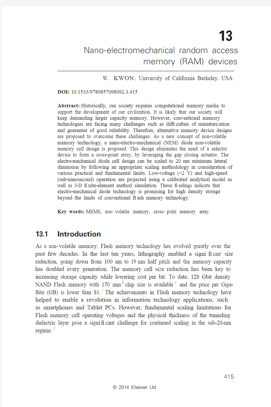
F igures 13.1 (a and b) illustrate the cell structure and the array layout of electro- mechanical diode memory. The bit lines (BLs) are formed on the insulating substrate and the word lines (WLs) are formed over the bit lines. The WLs and BLs are formed in different types (n- t ype or p- t ype) of semiconductor layer. Initially, the WLs are physically separated from the BLs by an air gap at each cross- p oint, so that no current can ? ow between these lines through the cell initially. This array
conFiguration can achieve the most ef ? cient cell layout area of 4F 2.
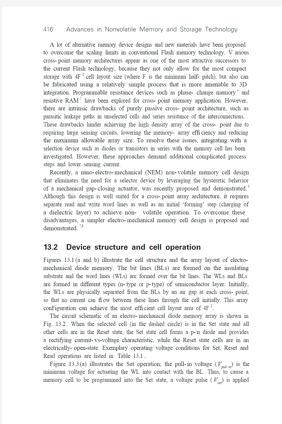
T he circuit schematic of an electro- m echanical diode memory array is shown in F ig. 13.2 . When the selected cell (in the dashed circle) is in the Set state and all other cells are in the Reset state, the Set state cell forms a p- n diode and provides a rectifying current- v s-voltage characteristic, while the Reset state cells are in an electrically- o pen-state. Exemplary operating voltage conditions for Set, Reset and Read operations are listed in T able 13.1 .
F igure 13.3 (a) illustrates the Set operation; the pull- i n voltage ( V p ull- i n ) is the minimum voltage for actuating the WL into contact with the BL. Thus, to cause a memory cell to be programmed into the Set state, a voltage pulse ( V
s et ) is applied
Nano-
e lectromechanical random access memory devices 417
13.1(a) Schematic cross- s ection of the electro- m echanical diode cell
(parallel to the word line); (b) schematic plan view of the electro-
mechanical diode memory array.
T able 13.1E xemplary voltage conditions for Set, Reset and Read operations. The selected word line (WL’) and selected bit line (BL’) are biased to achieve Set, Reset and Read operations
S et R eset R ead
W L’ (selected) 0 V 0 V V
read >0V
B L’ (selected) V
Set > V
pull- i n
V
Reset
< V
release
0 V
W L (unselected) (Floating)
(Floating)
0 V
B L (unselected) 0 V 0 V (Floating)
418 Advances in Non- v olatile Memory and Storage Technology
13.2 C ircuit schematic of an electro- m echanical diode memory array. between its WL and BL to induce an attractive electrostatic force that is suf ? ciently
larger than the pull- i n voltage ( V p ull- i n ). In order for the Set state to be retained during a Hold operation (i.e. when no voltage is applied), the built- i n electrostatic
force ( F e lect in F ig. 13.3 (b)) together with the surface adhesion force ( F a dhesion in F ig. 13.3 (b)) in the Set state must be larger than the spring restoring force ( F s pring in F ig.13.3 (b)) in the Set state.
T he state of a cell is determined by sensing the BL current when a Read voltage is applied between its WL and BL ( F ig. 13.4 (a)). If the cell is in the Reset state, no current ? ows through ( F ig.13.4 (b)); only leakage current (through parasitic paths) can ? ow. If the cell is in the Set state, a much larger forward diode current ? ows through.
A Reset operation is shown in F ig. 13.5 . To cause a memory cell to be erased into the Reset state, a voltage pulse ( V reset ) is applied between its WL and BL to counteract the built- i n electrostatic force of the p- n diode ( F ig. 13.5 (a)). When the sum of F e lect and F a dhesion becomes smaller than F s pring , the spring restoring force of
Nano- e lectromechanical random access memory devices 419
13.3 (a) Illustration of the Set operation. When V set is applied on the bit line (BL), the word line (WL) is pulled down to the BL by
electrostatic force. (b) Illustration of the Hold operation. The Set state
is sustained by a sum of electrostatic force ( F elect ) caused by space charges in the depletion region and surface adhesion force ( F adhesion ) between WL and BL materials; F spring < F elect + F adhesion
. the WL beam pulls it out of contact with the BL ( F ig. 13.5 (b)). After a Reset operation, the cell state is maintained due to a suf ? ciently stiff beam.
13.3 Fabrication process for a prototype cell
T he process used to fabricate the ? rst prototype electro- m echanical memory array is illustrated in F ig. 13.6 ; to form an isolation layer, 100 nm Al 2O 3 is coated on the silicon wafer by an Atomic Layer Deposition (ALD) tool at 350 °C. A phosphorus i n- s itu doped poly-Si (at 550 °C, 100 nm, 85 Ω /□) layer is deposited onto the insulating substrate (Al 2O 3 ), followed by a sacri ? cial oxide (LPCVD oxide 30 nm) deposition at 450 °C. After making photo resistor patterns of lines, the reactive ion etch (RIE) cuts into the oxide and poly-Si layer to form bit lines. A silicon- nitride (SiN x ) is deposited over the bit lines, and the SiN x
etch process forms
420 Advances in Non- v olatile Memory and Storage Technology
13.4 (a) Illustration of the Read operation in the Set state. The Read
current ? ows through the p- n junction when a forward bias ( V read ) is applied on the word line. (b) Illustration of the Read operation in the
Reset state. No current ? ows between the bit line (BL) and the word line (WL).
silicon- n itride spacers along the BLs; the silicon- n itride spacers provide anchor of the WLs beam and also electrical isolation between WLs and BLs. A boron i n- s itu -doped poly-Si 0.4G e 0.6 deposition (100 nm, 300 Ω /□) is deposited as the WLs material. After making photo resistor patterns of perpendicular lines to the BLs, the
RIE cuts into the poly-Si 0.4G e 0.6 layer and forms the WLs. Finally, the sacri ? cial oxide is selectively removed by vapor HF, which leaves air gaps between the
BLs and WLs.
S canning electron microscopy (SEM) images are shown in F igs 13.7 and 13.8 .
A bird’s- e ye view shows that the functional 4 μ m × 4 μ m cells are successfully fabricated in F ig. 13.7 . The cross- s ectional view shows the sacri ? cial oxide layer thickness (12.7 nm); the as- f abricated gap thickness between BL (n- t ype poly-Si) and WL (p- t ype poly-Si 0.4G e 0.6 ) is approximately 13 nm.
Nano- e lectromechanical random access memory devices 421
13.5 (a) Illustration of the Reset operation. As a forward bias ( V reset ) is applied on the p- n junction, the built- i n electrostatic force decreases. When the sum of the electrostatic force and the adhesion force is
smaller than the spring restoring force, the spring restoring force
pulls the WL beam out of the BL. (b) Illustration of the cell state after the Reset operation. The cell state (i.e. Reset state) is maintained due to a suf? ciently stiff beam after a Reset operation.
13.3.1 Electrical measurement of the prototype cell
F igure 13.9 shows the BL current changes of a prototype cell during a Set operation.
A sudden increase in current at the pull- i n voltage ( V p ull- i n = 6.2 V) is observed when the WL is pulled in to contact the BL. Since it is an applied voltage (not current) that is required to actuate the WL, the Set current can be lowered by inserting a current- l imiting resistance (1 M Ω) in series with the BL driver ( F ig. 13.7 ), to reduce the energy consumed by the Set operation. F igure 13.10 shows the transient response of the WL voltage during a Set operation. The measured set time for the prototype cell is approximately 2 μ s for a Set voltage of 14 V .
T o ‘Hold’ the Set state without applied voltage, the attraction forces (i.e. the summation of electrostatic force ( F e lect ) and adhesion force ( F
a dhesion )) between the
422 Advances in Non- v olatile Memory and Storage Technology
13.6K ey process steps for fabricating the prototype electro-
mechanical diode memory array: (a) n- t ype poly-Si and sacri? cial
oxide (LTO) layers deposition on the isolation oxide (Al
2O
3
); (b) bit
lines formation by photo lithography and reactive ion etch (RIE);
(c) silicon nitride (PECVD SiN
x ) deposition; (d) spacer formation;
(e) p-type poly-Si
0.4G e
0.6
deposition and WL formation; and
(f) sacri? cial oxide removal by vapor HF.
Nano- e lectromechanical random access memory devices 423
13.7 B ird’s eye SEM view of the fabricated electro- m echanical diode array. The working prototype memory cell size is 4 μ m × 4 μ m .
13.8 C ross- s ectional SEM image of the fabricated electro- m echanical diode before sacri? cial oxide removal by vapor HF. Since the oxide
thickness is 12.7 nm, the gap thickness after releasing poly-Si 0.4 G e 0.6 in vapor HF is ~13 nm.
424 Advances in Non- v
olatile Memory and Storage Technology
13.10 M easured transient voltages of WL and BL during Set operation of a prototype electro- m echanical diode cell. A step pulse of voltage is given on the BL and the voltage on WL is monitored by an
oscilloscope. When the WL touches the BL, the WL voltage increases rapidly at 2 μ s ec.
13.9 M easured Set operation hysteric I-V curves of a prototype
electro- m echanical diode cell as the bit line voltage is swept from 0 V to 8 V and 8 V to 0 V. After inserting a current- l imiting resistance
(1 M Ω ), the current can be lowered to reduce the power consumption of the Set operation.
Nano- e lectromechanical random access memory devices 425
WL and the BL has to be larger than the spring restoring force ( F s pring ) of the WL beam. The electrostatic force is caused by built- i n space charges in the deletion
region of the p- n diode. Finite element method simulation 9 is used for the proto-
type cell to calculate F e lect . F igure 13.11 shows the simulated energy band diagram and electric ? eld pro ? le for a p- n junction of the prototype cell and it gives the
value of F e lect to be 70.5 μ N . Since the calculate F s pring is only 4.22 μ N from another ? nite element method simulation, 10 the Set state is retained when the external
voltage (i.e. the actuation voltage) is removed
T he state of a cell is determined by sensing the BL current when the Read bias voltage is applied between its WL and BL. If the cell is in the Reset state, no
current ? ows through; only leakage current ? ows through the SiN x spacers in the cell. On the other hand, if the cell is in the Set state, a much larger current ? ows
through the forward- b iased p- n junction. F igure 13.12 shows measured I-V curves (linear scale and log scale of currents) in the Set and Reset state; a very high Set/
Reset current ratio (>10 6
) is seen. F igure 13.13 shows how the BL current of the prototype cell changes during a Reset operation. An abrupt drop in current at the release voltage ( V r elease =?6.2 V) is seen when the WL is released from the BL and goes back to the Reset state. It should be noted that the release voltage is larger than the ? at band voltage (~1
V in 13.11 S imulated energy- b and diagram and electric- ? eld pro? le within
a p- n junction in the Set state with V BL = 0 V and V WL = 0 V (Hold state). It is relevant to the prototype cell’s doping condition.
426 Advances in Non- v olatile Memory and Storage Technology
13.12(a) Measured I-V curves for Read operation of a prototype
electro- m echanical diode cell. A cell in the Set state shows a typical
p- n diode curve (black curve), whereas only leakage current is shown
in the Reset state cell (grey curve); and (b) measured log- s caled I-V
curves for Read operation of a prototype electro- m echanical cell.
Nano-
e lectromechanical random access memory devices 427
13.13M easured I-V curve for Reset operation of a prototype electro-
mechanical diode cell. The bit line voltage is swept from 0 V to ?8 V to
increase forward- b ias on the p- n junction.
13.14M easured Reset time of a prototype electro- m echanical diode
cell, where the bit line voltage is ?7 V and the word line voltage is 0 V
(a forward bias condition on the p- n junction).
428 Advances in Non- v olatile Memory and Storage Technology
ideal case) of a p- n diode in a forward bias condition. The large release voltage is caused by the voltage drop on the WL and BL. Since the thickness of the WL beam is thin, the resistance of the WL is too large, which results in a large voltage drop on the WL rather than the p- n junction. To reduce these voltage drops on the external resistance, a metallic WL material, or shunting it with a metal layer, can be usable.
F rom transient measurements, the reset time for the prototype cell is approximately 100 ms for a Reset voltage of ?7 V ( F ig. 13.14 ). The longer reset time possibly can
be explained by the contact opening model presented in, 11 the restoring spring force
reduces the number of bonds between the contacting surfaces ( F ig. 13.15 ); only when the number of bonds is suf ? ciently small, can contact opening occur. The contact opening time therefore depends on the number of bonds formed between the contacting surfaces, and can be reduced with scaling (to reduce the contact force and apparent contact area) and/or an appropriate surface treatment.
13.3.2 Suppression of sneak leakage currents in the cell array
A key requirement for implementation of a cross- p oint memory array is the suppression of the unwanted ‘sneak’ leakage currents through unselected cells in the array. These leakages can sum to a suf ? ciently high current to result in an
erroneous Read operation. 12 The size of the cross- p oint array is therefore limited
by the ratio of the selected cell current to the summation of the leakage currents
of unselected cells in the Set state during a Read operation;
13 the larger this ratio, the larger the array size. The sneak leakage current through unselected cell in the Set state is almost equal to the diode current in a reverse- b iased condition, which is one- h alf the forward- b ias read voltage ( V W L,READ ) for an optimally designed sense ampli ? er for a resistive cross- p oint memory array. Thus, the ratio of the forward- b ias Set cell current at V W L,READ to the reverse- b ias Set cell current at – V W L,READ /2, ‘the recti ? cation ratio’, is a key parameter to determine cross- p oint
array size.
13.15 I llustration of the p- n junction (contacting surfaces) of the
electro- m echanical diode.
Nano- e lectromechanical random access memory devices 429
T he recti ? cation ratio of the prototype cell is approximately 300 for V W L,READ = 1.2 V . It can be enhanced by increasing the work- f unction difference between the WL and BL materials and by improving crystalline quality of the semiconductor materials. F igure 13.16 shows the demonstrated experiment results of p- t ype poly-Si as the WL material and adding a thermal anneal step. T able 13.2 also shows the ideal factor and recti ? cation ratio changes of the p- n diode curves of each p- t ype poly-Si process condition; since the p- t ype poly-Si has a larger
work function than p- t ype poly-Si 0.4G e 0.6 , the recti ? cation ratio has been improved almost three times. Furthermore, the recti ? cation ratio is improved greatly and the
diode curve is getting close to the ideal diode curve, due to the thermal annealing step for increasing average grain size improving.
T able 13.2 M easured electro- m echanical diode characteristics for different p- t ype WL materials and post- d eposition annealing conditions
P -type WL material
N on- i deal factor R ecti? cation ratio P oly-Si 0.4 Ge 0.6 (410 °C) 5 ~ 8 50
P oly-Si (610 °C) with 950 °C, 1 hr anneal
3.0 10 3
P oly-Si (610 °C) with 1050 °C, 1 hr anneal 1.7 10 4
13.16 M easured diode I-V curves of electro- m echanical diode cell of poly-Si word line case with post annealing conditions.
430 Advances in Non- v olatile Memory and Storage Technology
13.17M easured retention behavior of a prototype electro- m echanical
diode cell in the Set state (circles) and the Reset state (squares) in the
high temperature condition (200 °C).
13.18M easured endurance characteristics of a proto t ype electro-
mechanical diode cell in the Set state (circles) and the Reset state
(squares).
Nano- e lectromechanical random access memory devices 431 13.4 Assessing cell reliability
I n order to investigate the basic reliability of the prototype cell, data retention and endurance are measured. Since surface adhesion force and electrostatic force hold a diode memory cell in the Set state, the prototype cell shows very long retention time in F ig. 13.17 ; negligible changes in conductance for the Set and Reset states are seen at 200 °C, which well exceeds the normal operating temperature range for CMOS. As the electro- m echanical diode does not rely on charge storage in a ? oating- g ate/charge- t rap layer or a material phase change to store data, it has more robust retention behavior than other NVM technologies. Moreover, it opens the possibility for new applications that demand very high (>150 °C) temperature operating.
F igure 13.18 shows that the prototype cell is multi- t ime programmable (MTP),
with endurance exceeding 10 4 Set/Reset cycles. The endurance of an electro-
mechanical device can be very high if it is properly designed. For example, the
endurance of a micro- e lectro- m echanical switch has been shown to exceed 10 9
on/off cycles. 14
A potential reliability concern for mechanical devices is vibration or mechanical shock. But because of the extremely small mass (3.73 picogram for the prototype
devices in this work) of the WL beam within a cell, a very large acceleration (10 8G)
would be needed to accidentally Set a cell or to overcome the attraction forces in the Set state (4 μ N for the prototype devices in this work) to Reset a cell. This is far
beyond the acceleration requirement (~20 000 G) for automotive environments. 15
13.5 Device scaling
A
shrinking device area is required for high storage density memory application. For the scaling of electrostatically actuated beams, a constant- ? eld scaling
methodology is used. 16 Also, to achieve non- v olatility in the Hold state (i.e.
without an external bias, the built- i n electrostatic force ( F e lect ), the Set state has to be larger than the spring restoring force ( F s pring ) in the Set state. Following this methodology, the beam thickness and actuation gap thickness should be scaled
down together with the lateral dimensions of the beam, to reduce the Set voltage (i.e. Vpull- i n) and operation energy. Since there is a practical limit for beam thickness scaling, alternative structural materials with lower Young’s modulus can be used to reduce beam stiffness.
P rojected pull- i n voltages for nanometer- s cale diode memory cells are shown
in T able 13.3 . These were calculated using Finite-Element-Method software 10 and
for various conductive structural materials with lower Young’s modulus, for
example TiNi alloy 17 and carbon nanotube (CNT); 18 note that the scaling of beam
length is legged behind the beam with scaling, because the restoring force (the
spring force) increases greatly. Thus, the device area becomes larger than 4F 2.
T able 13.4 shows the performances and cell size comparisons between the scaled electro- m echanical diode cell and the current and emerging non- v olatile memory
cells around 20 nm technologies. 19 The electro- m echanical diode technology shows
432 Advances in Non- v olatile Memory and Storage Technology advantages, including compatible cell size, simplest process, good retention (even at high temperature) and lowest energy consumption for programming. Therefore the electro- m echanical diode potentially can be a good candidate for non- v olatile memory solution beyond the limitations of other technologies.
13.6 Conclusion
A new electro- m echanical diode memory cell is proposed for the cross- p oint non- volatile memory array application. The ? rst prototype cell demonstrates the basic T able 13.4 C omparison of scaled electro-mechanical diode technology with current and emerging technologies at 16 nm technology generation in reference 19 T echnology N AND Flash P CM R edox RRAM E
lectro-mechanical
diode device
E ffective cell size (per bit) 2.5
F 2 4 ~ 6F 2 5 ~ 8 F 2 4 ~ 6 F 2
M inimum F-scaling 16 nm 5 ~ 10 nm 5 ~ 10 nm 20 nm
W rite voltage 18 ~ 20 V 3 V < 0.5 V
2.4 V
W rite speed >10 nsec 50 ~ 120 nsec <20 nsec 0.27 nsec R etention 10 yrs at 85°C ~ 4 days at 125°C 10 yrs at 85°C < 1 day at 125°C 10 yrs at 85° ~ 2 days at 125°C
> 10 yrs at 200°C
E ndurance 10
4 ~ 10
5 10 15 10 1
6 >10 4 P rogramming energy per bit
> 1 fJ
< 2pJ 1 fJ 0.03 fJ
E ase of integration 10 Masks 2 ~ 3 Masks to BEOL 2 ~ 3 Masks to BEOL
2 Masks T able 13.
3 D esign and calculated performance characteristics of scaled electro- mechanical diode memory cells
T echnology 4 μ m 40 nm 20 nm 10 nm
C ell size 64 μ m 2 0.0064 μ m 2 0.0016 μ m 2 0.0008 μ m 2
B eam width 4 μ m 40 nm 20 nm 10 nm B eam length 4 μ m 40 nm 30 nm 20 nm F 2 4 F 2 4 F 2 6 F 2 8 F 2
S tructural material P oly-SiGe T iNi T iNi C NT Y oung’s modulus 140 GPa 14 GPa 14 GPa 5 GPa B eam thickness 100 nm 5 nm 4 nm 3 nm A ctual gap thickness 35 nm
(*13 nm) 3 nm 2 nm 2 nm
S et voltage 7.0 V 3.5 V 2.4 V 2.1 V S et time 2 us 0.38 ns 0.27 ns 0.12 ns
E nergy for set operation 2.6 × 10 ?13 J
7.8 × 10 ?17 J 2.7 × 10 ?17 J 5.4 × 10 ?18 J
e lectromechanical random access memory devices 433 Nano-
idea with relatively low Set/Reset voltages. It also shows excellent retention behavior and multi- t ime programmable exceeding 10 4cycles, so that this design shows promise for compact and low power operating non- v olatile storage applications in the future.
13.7 References
1. L i ,Y. e t al. ( 2012 ), ‘ 128 Gb 3b/Cell NAND Flash memory in 19 nm technology with
18MB/s write rate and 400 Mb/s toggle mode ’, S olid-State Circuits Conference Digest of Technical Papers( I SSCC).
2. 64 Giga bit NAND Flash price on :w https://www.doczj.com/doc/8010858108.html,[ a ccessed 1/28 /2013 ].
3. K oh ,Y. ( 2009 ), ‘ N AND Flash scaling beyond 20 nm ’, I nternational Memory Workshop.
4. W ong ,H.-S.P. ,R aoux ,S. ,K im ,S. ,L iang ,J. ,R eifenberg ,J.P. e t al.( 2010 ), ‘ P hase
change memory ’, P roc. IEEE,98 (12 ): 2201 –27 .
5. A kinaga ,H. and S hima ,H. ( 2010 ), ‘ R esistive random access memory (ReRAM) based
on metal oxides ’, P roc. IEEE,98 (12 ): 2237 –51 .
6. C hoi ,W.Y. ,K am ,H. ,L ee ,D. ,L ai ,J. and L iu ,T.-J.K. ( 2007 ), ‘ C ompact nano- e lectro-
mechanical non- v olatile memory (NEMory) for 3D integration ’. I EDM Tech. Dig., 603 –6.
7. K won ,W. ,J eon ,J. ,H utin ,L. and L iu ,T.K. ( 2012 ), ‘ E lectro- m echanical diode memory
cell design for cross- p oint memory arrays ’, I EEE Electron Device Letters,33 (2).
8. K won ,W. ,H utin ,L. and L iu ,T-J.K. ( 2012 ). ‘ E lectro-mechanical diode performance
and scaling for cross- p oint non- v olatile memory array ’, I nternational Memory Workshop( I MW).
9. S entaurus Ver. A-2008.09, SYNOPSYS.
10. C oventorWare? Ver. 2008 .
11. J ensen ,B.D. ,H uang ,K. ,C how ,L.L.-W. and K urabayashi ,K. ( 2005 ), ‘ A dhesion
effects on contact opening dynamics in micromachined switches ’, J ournal of Applied Physics,97 :103535 .
12. L iang ,J. and W ong ,H.-S.P. ( 2010 ), ‘ C ross- p oint memory array without cell selectors:
device characteristics and data storage pattern dependencies ’, I EEE Transaction on Electron Devices,57 :2531 .
13. F locke ,A. and N oll ,T.G. ( 2007 ), ‘ F undamental Analysis of Resistive Nano-Crossbars
for the Use in Hybrid Nano/CMOS-Memory ’, I nternational Solid-State Circuits Conference Digest,328 .
14. K am ,H. ,P ott ,V. ,N athanael ,R. ,J eon ,J. ,A lon ,E. e t al.( 2009 ), ‘ D esign and reliability
of a micro- r elay technology for zero- s tandby-power digital logic applications ’, I EEE IEDM Technical Digest.
15. A utomotive Electronic Council ( 2007 ), A EC-Q100-Rev-G ,14 M ay .
16. C hen ,F. ,K am ,H. ,M arkovic ,D. ,L iu ,T-J.K. ,S tojanovic ,V. e t al.( 2008 ), ‘ I ntegrated
circuit design with NEM relays ’, I CCAD,p. 750 .
17. L ee ,D. ,O sabe ,T. and L iu ,T-J.K. ( 2009 ), ‘ S caling limitations for ? exural beams used
in electromechanical devices ’, I EEE Transactions on Electron Devices,56 :688 .
18. A cquavia ,D. e t al.( 2010 ), ‘ C apacitive nanoelectromechanical switch based on
suspended carbon nanotube array ’, A pplied Physics Letters,97 :233508.
19. Assessment of the Potential and Maturity of Selected Emerging Research Memory
Technologies Workshop and ERD/ERM Working Group Meeting, 6–7 April, ITRS.