MC10H116
Triple Line Receiver
Description
The MC10H116 is a triple differential amplifier designed for use in sensing differential signals over long lines and is a functional/pinout duplication of the MC10116, with 100% improvement in propagation delay and no increase in power supply current. For termination information see AND8020.
Features
?Propagation Delay, 1.0 ns Typical
?Power Dissipation 85 mW Typ/Pkg (same as MECL 10K ?)?Improved Noise Margin 150 mV (Over Operating V oltage and Temperature Range)?V oltage Compensated ?MECL 10K Compatible
?
Pb ?Free Packages are Available*
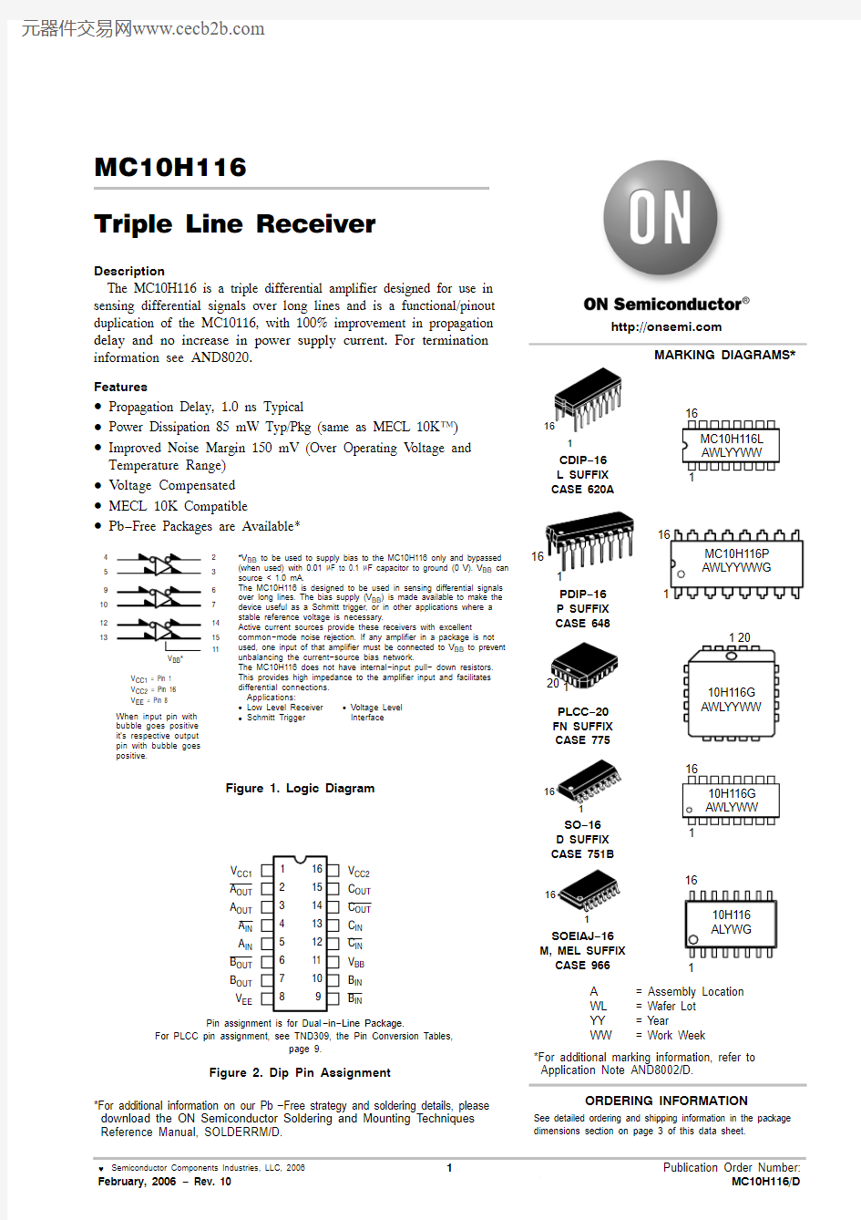
Figure 1. Logic Diagram
*V BB to be used to supply bias to the MC10H116 only and bypassed (when used) with 0.01 m F to 0.1 m F capacitor to ground (0 V). V BB can source < 1.0 mA.
The MC10H116 is designed to be used in sensing differential signals over long lines. The bias supply (V BB ) is made available to make the device useful as a Schmitt trigger, or in other applications where a stable reference voltage is necessary.
Active current sources provide these receivers with excellent
common ?mode noise rejection. If any amplifier in a package is not used, one input of that amplifier must be connected to V BB to prevent unbalancing the current ?source bias network.
The MC10H116 does not have internal ?input pull ? down resistors.This provides high impedance to the amplifier input and facilitates differential connections.Applications:
?Low Level Receiver ?Voltage Level ?Schmitt Trigger Interface
Figure 2. Dip Pin Assignment
V CC1A OUT A OUT A IN A IN B OUT B OUT V EE
V CC2C OUT C OUT C IN C IN V BB B IN B IN
161514131211109
12345678
5411
321097613
121514When input pin with bubble goes positive it’s respective output pin with bubble goes positive.
V CC1 = Pin 1V CC2 = Pin 16V EE = Pin 8BB Pin assignment is for Dual ?in ?Line Package.
For PLCC pin assignment, see TND309, the Pin Conversion Tables,
page 9.
*For additional information on our Pb ?Free strategy and soldering details, please download the ON Semiconductor Soldering and Mounting Techniques Reference Manual, SOLDERRM/D.
https://www.doczj.com/doc/8112111236.html,
See detailed ordering and shipping information in the package dimensions section on page 3 of this data sheet.
ORDERING INFORMATION
Table 1. MAXIMUM RATINGS
Symbol Characteristic Rating Unit V EE Power Supply (V CC = 0)?8.0 to 0Vdc V I Input Voltage (V CC = 0)0 to V EE Vdc
I out Output Current? Continuous
? Surge 50
100
mA
T A Operating Temperature Range0 to +75°C
T stg Storage Temperature Range? Plastic
? Ceramic ?55 to +150
?55 to +165
°C
°C
Maximum ratings are those values beyond which device damage can occur. Maximum ratings applied to the device are individual stress limit values (not normal operating conditions) and are not valid simultaneously. If these limits are exceeded, device functional operation is not implied, damage may occur and reliability may be affected.
Table 2. ELECTRICAL CHARACTERISTICS (V EE = ?5.2 V ±5%) (Note 2)
0°25°75°
Symbol Characteristic Min Max Min Max Min Max Unit
I E Power Supply Current?23?21?23mA
I inH Input Current High?150?95?95m A
I CBO Input Leakage Current? 1.5? 1.0? 1.0m A
V BB Reference Voltage?1.38?1.27?1.35?1.25?1.31?1.19Vdc
V OH High Output Voltage?1.02?0.84?0.98?0.81?0.92?0.735Vdc
V OL Low Output Voltage?1.95?1.63?1.95?1.63?1.95?1.60Vdc
V IH High Input Voltage (Note 1)?1.17?0.84?1.13?0.81?1.07?0.735Vdc
V IL Low Input Voltage (Note 1)?1.95?1.48?1.95?1.48?1.95?1.45Vdc
V CMR Common Mode Range (Note 4)???2.85 to ?0.8??Vdc
V PP Input Sensitivity (Note 3)??150 typ??mV PP
1.When V BB is used as the reference voltage.
2.Each MECL 10H? series circuit has been designed to meet the specifications shown in the test table, after thermal equilibrium has been
established. The circuit is in a test socket or mounted on a printed circuit board and transverse air flow greater than 500 linear fpm is maintained. Outputs are terminated through a 50?ohm resistor to ?2.0 V.
3.Differential input not to exceed 1.0 Vdc.
4.150 mV p?p differential input required to obtain full logic swing on output.
Table 3. AC CHARACTERISTICS
0°25°75°
Symbol Characteristic Min Max Min Max Min Max Unit
t pd Propagation Delay0.4 1.30.4 1.30.45 1.45ns
t r Rise Time0.5 1.50.5 1.60.5 1.7ns
t f Fall Time0.5 1.50.5 1.60.5 1.7ns NOTE:Device will meet the specifications after thermal equilibrium has been established when mounted in a test socket or printed circuit board with maintained transverse airflow greater than 500 lfpm. Electrical parameters are guaranteed only over the declared
operating temperature range. Functional operation of the device exceeding these conditions is not implied. Device specification limit values are applied individually under normal operating conditions and not valid simultaneously.
ORDERING INFORMATION
Device Package Shipping?
MC10H116D SO?1648 Units / Rail
48 Units / Rail
MC10H116DG SO?16
(Pb?Free)
MC10H116DR2SO?162500 / Tape & Reel
2500 / Tape & Reel
MC10H116DR2G SO?16
(Pb?Free)
MC10H116FN PLCC?2046 Units / Rail
46 Units/Rail
MC10H116FNG PLCC?20
(Pb?Free)
MC10H116FNR2PLCC?20500 / Tape & Reel
500 / Tape & Reel
MC10H116FNR2G PLCC?20
(Pb?Free)
MC10H116L CD1P?1625 Units / Rail
MC10H116M SOEIAJ?1650 Units / Rail
50 Units / Rail
MC10H116MG SOEIAJ?16
(Pb?Free)
MC10H116MEL SOEIAJ?162000 / Tape & Reel
2000 / Tape & Reel
MC10H116MELG SOEIAJ?16
(Pb?Free)
MC10H116P PD1P?1625 Units / Rail
MC10H116PG PD1P?16
25 Units / Rail
(Pb?Free)
?For information on tape and reel specifications,including part orientation and tape sizes, please refer to our Tape and Reel Packaging Specifications Brochure, BRD8011/D.
PACKAGE DIMENSIONS
S
L?M
S 0.010 (0.250) N
S
T 20 LEAD PLLC CASE 775?02ISSUE E
NOTES:
1.DIMENSIONS AND TOLERANCING PER ANSI Y14.5M,198
2.
2.DIMENSIONS IN INCHES.
3.DATUMS ?L ?, ?M ?, AND ?N ? DETERMINED WHERE TOP OF LEAD SHOULDER EXITS PLASTIC BODY AT MOLD PARTING LINE.
4.DIMENSION G1, TRUE POSITION TO BE MEASURED AT DATUM ?T ?, SEATING PLANE.
5.DIMENSIONS R AND U DO NOT INCLUDE MOLD FLASH.ALLOWABLE MOLD FLASH IS 0.010 (0.250) PER SIDE.
6.DIMENSIONS IN THE PACKAGE TOP MAY BE SMALLER THAN THE PACKAGE BOTTOM BY UP TO 0.012 (0.300).DIMENSIONS R AND U ARE DETERMINED AT THE OUTERMOST EXTREMES OF THE PLASTIC BODY EXCLUSIVE OF MOLD FLASH, TIE BAR BURRS, GATE BURRS AND INTERLEAD FLASH, BUT INCLUDING ANY MISMATCH BETWEEN THE TOP AND BOTTOM OF THE PLASTIC BODY .
7.DIMENSION H DOES NOT INCLUDE DAMBAR PROTRUSION OR INTRUSION. THE DAMBAR
PROTRUSION(S) SHALL NOT CAUSE THE H DIMENSION TO BE GREATER THAN 0.037 (0.940). THE DAMBAR
INTRUSION(S) SHALL NOT CAUSE THE H DIMENSION TO BE SMALLER THAN 0.025 (0.635).
DIM MIN MAX MIN MAX MILLIMETERS
INCHES A 0.3850.3959.7810.03B 0.3850.3959.7810.03C 0.1650.180 4.20 4.57E 0.0900.110 2.29 2.79F 0.0130.0190.330.48G 0.050 BSC 1.27 BSC H 0.0260.0320.660.81J 0.020???0.51???K 0.025???0.64???R 0.3500.3568.899.04U 0.3500.3568.899.04V 0.0420.048 1.07 1.21W 0.0420.048 1.07 1.21X 0.0420.056 1.07 1.42Y ???0.020???0.50Z 2 10 2 10 G10.3100.3307.888.38K1
0.040???
1.02???
____
PACKAGE DIMENSIONS
CDIP ?16L SUFFIX
CERAMIC DIP PACKAGE
CASE 620A ?01ISSUE O
NOTES:
1.DIMENSIONING AND TOLERANCING PER ASME Y14.5M, 1994.
2.CONTROLLING DIMENSION: INCH.
3.DIMENSION L TO CENTER OF LEAD WHEN FORMED PARALLEL.
4.DIMENSION F MAY NARROW TO 0.76 (0.030)WHERE THE LEAD ENTERS THE CERAMIC BODY.
5THIS DRAWING REPLACES OBSOLETE CASE OUTLINE 620?10.
DIM MIN MAX MIN MAX MILLIMETERS
INCHES A 0.7500.78519.0519.93B 0.2400.295 6.107.49C ???0.200??? 5.08D 0.0150.0200.390.50E 0.050 BSC 1.27 BSC F 0.0550.065 1.40 1.65G 0.100 BSC 2.54 BSC H 0.0080.0150.210.38K 0.1250.170 3.18 4.31L 0.300 BSC 7.62 BSC M 0 15 0 15 N
0.0200.040
0.51 1.01
____NOTES:
1.DIMENSIONING AND TOLERANCING PER ANSI Y14.5M, 198
2.
2.CONTROLLING DIMENSION: INCH.
3.DIMENSION L TO CENTER OF LEADS WHEN FORMED PARALLEL.
4.DIMENSION B DOES NOT INCLUDE MOLD FLASH.
5.ROUNDED CORNERS OPTIONAL.
DIM MIN MAX MIN MAX MILLIMETERS
INCHES A 0.7400.77018.8019.55B 0.2500.270 6.35 6.85C 0.1450.175 3.69 4.44D 0.0150.0210.390.53F 0.0400.70 1.02 1.77G 0.100 BSC 2.54 BSC H 0.050 BSC 1.27 BSC J 0.0080.0150.210.38K 0.1100.130 2.80 3.30L 0.2950.3057.507.74M 0 10 0 10 S
0.0200.040
0.51 1.01
____
PACKAGE DIMENSIONS
SO ?16D SUFFIX
NOTES:
1.DIMENSIONING AND TOLERANCING PER ANSI Y14.5M, 198
2.
2.CONTROLLING DIMENSION: MILLIMETER.
3.DIMENSIONS A AND B DO NOT INCLUDE MOLD PROTRUSION.
4.MAXIMUM MOLD PROTRUSION 0.15 (0.006)PER SIDE.
5.DIMENSION D DOES NOT INCLUDE DAMBAR PROTRUSION. ALLOWABLE DAMBAR
PROTRUSION SHALL BE 0.127 (0.005) TOTAL IN EXCESS OF THE D DIMENSION AT MAXIMUM MATERIAL CONDITION.
S
B
M
0.25 (0.010)A
S
T DIM MIN MAX MIN MAX INCHES
MILLIMETERS A 9.8010.000.3860.393B 3.80 4.000.1500.157C 1.35 1.750.0540.068D 0.350.490.0140.019F 0.40 1.250.0160.049G 1.27 BSC 0.050 BSC J 0.190.250.0080.009K 0.100.250.0040.009M 0 7 0 7 P 5.80 6.200.2290.244R
0.250.50
0.0100.019
____SOEIAJ ?16CASE 966?01ISSUE A
NOTES:
1.DIMENSIONING AND TOLERANCING PER ANSI Y14.5M, 198
2.
ON Semiconductor and are registered trademarks of Semiconductor Components Industries, LLC (SCILLC). SCILLC reserves the right to make changes without further notice to any products herein. SCILLC makes no warranty, representation or guarantee regarding the suitability of its products for any particular purpose, nor does SCILLC assume any liability arising out of the application or use of any product or circuit, and specifically disclaims any and all liability, including without limitation special, consequential or incidental damages.“Typical” parameters which may be provided in SCILLC data sheets and/or specifications can and do vary in different applications and actual performance may vary over time. All operating parameters, including “Typicals” must be validated for each customer application by customer’s technical experts. SCILLC does not convey any license under its patent rights nor the rights of others. SCILLC products are not designed, intended, or authorized for use as components in systems intended for surgical implant into the body, or other applications intended to support or sustain life, or for any other application in which the failure of the SCILLC product could create a situation where personal injury or death may occur. Should Buyer purchase or use SCILLC products for any such unintended or unauthorized application, Buyer shall indemnify and hold SCILLC and its officers, employees, subsidiaries, affiliates,and distributors harmless against all claims, costs, damages, and expenses, and reasonable attorney fees arising out of, directly or indirectly, any claim of personal injury or death associated with such unintended or unauthorized use, even if such claim alleges that SCILLC was negligent regarding the design or manufacture of the part. SCILLC is an Equal Opportunity/Affirmative Action Employer. This literature is subject to all applicable copyright laws and is not for resale in any manner.
PUBLICATION ORDERING INFORMATION
MECL 10H and MECL 10K are trademarks of Motorola, Inc.