1Chapter 4 Problem Set
Chapter 4
Problems
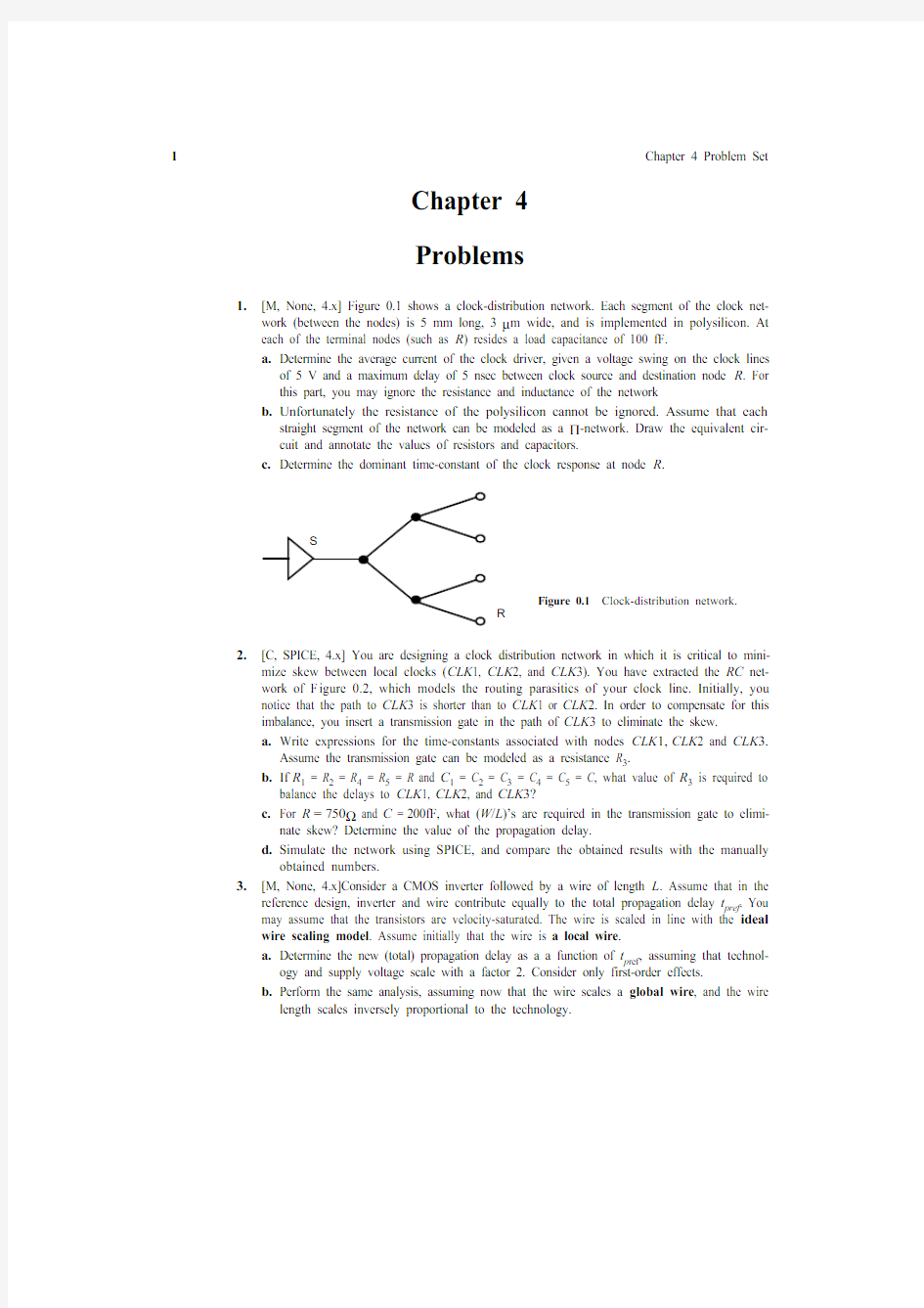
1.[M, None, 4.x] Figure 0.1 shows a clock-distribution network. Each segment of the clock net-
work (between the nodes) is 5 mm long, 3 μm wide, and is implemented in polysilicon. At
each of the terminal nodes (such as R ) resides a load capacitance of 100 fF.
a.Determine the average current of the clock driver, given a voltage swing on the clock lines
of 5 V and a maximum delay of 5 nsec between clock source and destination node R . For
this part, you may ignore the resistance and inductance of the network
b.Unfortunately the resistance of the polysilicon cannot be ignored. Assume that each
straight segment of the network can be modeled as a Π-network. Draw the equivalent cir-
cuit and annotate the values of resistors and capacitors.
c.Determine the dominant time-constant of the clock response at node R .
2.
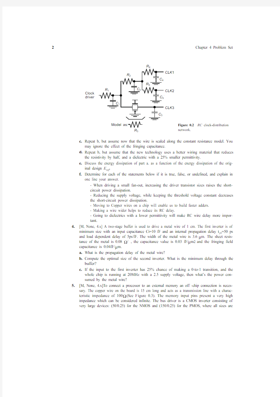
[C, SPICE, 4.x] You are designing a clock distribution network in which it is critical to mini-mize skew between local clocks (CLK 1, CLK 2, and CLK 3). You have extracted the RC net-work of F igure 0.2, which models the routing parasitics of your clock line. Initially, you notice that the path to CLK 3 is shorter than to CLK 1 or CLK 2. In order to compensate for this imbalance, you insert a transmission gate in the path of CLK 3 to eliminate the skew.a.Write expressions for the time-constants associated with nodes CLK 1,CLK 2 and CLK 3.Assume the transmission gate can be modeled as a resistance R 3.b.If R 1 = R 2 = R 4 = R 5 = R and C 1 = C 2 = C 3 = C 4 = C 5 = C , what value of R 3 is required to balance the delays to CLK 1, CLK 2, and CLK 3?c.For R =750Ω and C =200fF, what (W /L )’s are required in the transmission gate to elimi-nate skew? Determine the value of the propagation delay.d.Simulate the network using SPICE, and compare the obtained results with the manually obtained numbers.3.[M, None, 4.x]Consider a CMOS inverter followed by a wire of length L . Assume that in the
reference design, inverter and wire contribute equally to the total propagation delay t pref . You
may assume that the transistors are velocity-saturated. The wire is scaled in line with the ideal
wire scaling model . Assume initially that the wire is a local wire .
a.Determine the new (total) propagation delay as a a function of t p ref , assuming that technol-
ogy and supply voltage scale with a factor 2. Consider only first-order effects.
b.Perform the same analysis, assuming now that the wire scales a global wire , and the wire length scales inversely proportional to the technology.
Figure 0.1Clock-distribution network.
S
R
2Chapter 4 Problem Set
c.Repeat b, but assume now that the wire is scaled along the constant resistance model. You may ignore the effect of the fringing capacitance.
d.Repeat b, but assume that the new technology uses a better wiring material that reduces the resistivity by half, and a dielectric with a 25% smaller permittivity.
e.Discuss the energy dissipation of part a. as a function of the energy dissipation of the orig-inal design E ref .
f.Determine for each of the statements below if it is true, false, or undefined, and explain in one line your answer. - When driving a small fan-out, increasing the driver transistor sizes raises the short-circuit power dissipation. - Reducing the supply voltage, while keeping the threshold voltage constant decreases the short-circuit power dissipation.- Moving to Copper wires on a chip will enable us to build faster adders.- Making a wire wider helps to reduce its RC delay.- Going to dielectrics with a lower permittivity will make RC wire delay more impor-tant.4.
[M, None, 4.x] A two-stage buffer is used to drive a metal wire of 1 cm. The first inverter is of minimum size with an input capacitance Ci=10 fF and an internal propagation delay t p0=50 ps and load dependent delay of 5ps/fF. The width of the metal wire is 3.6 μm. The sheet resis-tance of the metal is 0.08 Ω/, the capacitance value is 0.03 fF/μm 2and the fringing field capacitance is 0.04fF/μm.a.What is the propagation delay of the metal wire?https://www.doczj.com/doc/8e9440837.html,pute the optimal size of the second inverter. What is the minimum delay through the buffer?c.If the input to the first inverter has 25% chance of making a 0-to-1 transition, and the whole chip is running at 20MHz with a 2.5 supply voltage, then what’s the power con-sumed by the metal wire?5.[M, None, 4.x]To connect a processor to an external memory an off -chip connection is neces-
sary. The copper wire on the board is 15 cm long and acts as a transmission line with a charac-
teristic impedance of 100Ω.(See F igure 0.3). The memory input pins present a very high
impedance which can be considered infinite. The bus driver is a CMOS inverter consisting of
very large devices: (50/0.25) for the NMOS and (150/0.25) for the PMOS, where all sizes are
Clock CLK 1CLK 2CLK 3R 1
R 2
R 5
R 4
R 3Model as:
Figure 0.2RC clock-distribution network.driver C 1
C 3
C 4
C 5C 2
Digital Integrated Circuits - 2nd Ed3 in μm. The minimum size device, (0.25/0.25) for NMOS and (0.75/0.25) for PMOS, has the
on resistance 35 kΩ.
a.Determine the time it takes for a change in the signal to propagate from source to destina-
tion (time of flight). The wire inductance per unit length equals 75*10-8 H/m.
b.Determine how long it will take the output signal to stay within 10% of its final value. You
can model the driver as a voltage source with the driving device acting as a series resis-
tance. Assume a supply and step voltage of 2.5V. Hint: draw the lattice diagram for the
transmission line.
c.Resize the dimensions of the driver to minimize the total delay.
L=15cm
Memory
Z=100Ω
Figure 0.3The driver, the connecting copper wire and the
memory block being accessed.
6.[M, None, 4.x] A two stage buffer is used to drive a metal wire of 1 cm. The first inverter is a
minimum size with an input capacitance C i=10 fF and a propagation delay t p0=175 ps when
loaded with an identical gate. The width of the metal wire is 3.6 μm. The sheet resistance of
the metal is 0.08 Ω/, the capacitance value is 0.03 fF/μm2 and the fringing field capacitance
is 0.04 fF/μm.
a.What is the propagation delay of the metal wire?
https://www.doczj.com/doc/8e9440837.html,pute the optimal size of the second inverter. What is the minimum delay through the
buffer?
7.[M, None, 4.x] For the RC tree given in Figure 0.4 calculate the Elmore delay from node A to
node B using the values for the resistors and capacitors given in the below in Table 0.1.
Figure 0.4RC tree for calculating the delay
4Chapter 4 Problem Set
Table 0.1Values of the components in the RC tree of Figure 0.4
Resistor Value(Ω)Capacitor Value(fF)
R10.25C1250
R20.25C2750
R30.50C3250
R4100C4250
R50.25C51000
R6 1.00C6250
R70.75C7500
R81000C8250
8.[M, SPICE, 4.x] In this problem the various wire models and their respective accuracies will
be studied.
https://www.doczj.com/doc/8e9440837.html,pute the 0%-50% delay of a 500um x 0.5um wire with resistance of 0.08 Ω/,with
area capacitance of 30aF/um2, and fringing capacitance of 40aF/um. Assume the driver
has a 100Ω resistance and negligible output capacitance.
?Using a lumped model for the wire.
?Using a PI model for the wire, and the Elmore equations to find tau. (see Chapter 4, figure
4.26).
?Using the distributed RC line equations from Chapter 4, section 4.4.4.
https://www.doczj.com/doc/8e9440837.html,pare your results in part a. using spice (be sure to include the source resistance). For
each simulation, measure the 0%-50% time for the output
?First, simulate a step input to a lumped R-C circuit.
?Next, simulate a step input to your wire as a PI model.
?Unfortunately, our version of SPICE does not support the distributed RC model as described in your book (Chapter 4, section 4.5.1). Instead, simulate a step input to your
wire using a PI3 distributed RC model.
9.[M, None, 4.x] A standard CMOS inverter drives an aluminum wire on the first metal layer.
Assume Rn=4kΩ, Rp=6kΩ. Also, assume that the output capacitance of the inverter is negli-
gible in comparison with the wire capacitance. The wire is .5um wide, and the resistivity is
0.08 Ω/..
a.What is the "critical length" of the wire?
b.What is the equivalent capacitance of a wire of this length? (For your capacitance calcula-
tions, use Table 4.2 of your book , assume there’s field oxide underneath and nothing
above the aluminum wire)
Digital Integrated Circuits - 2nd Ed
510.[M, None, 4.x] A 10cm long lossless transmission line on a PC board (relative dielectric con-
stant = 9, relative permeability = 1) with characteristic impedance of 50Ω is driven by a 2.5V
pulse coming from a source with 150Ω resistance.
a.If the load resistance is infinite, determine the time it takes for a change at the source to
reach the load (time of flight).
Now a 200Ω load is attached at the end of the transmission line.
b.What is the voltage at the load at t = 3ns?
c.Draw lattice diagram and sketch the voltage at the load as a function of time. Determine
how long does it take for the output to be within 1 percent of its final value.
11.[C, SPICE, 4.x] Assume V DD =1.5V . Also, use short-channel transistor models forhand analy-
sis.
a.The Figure 0.5 shows an output driver feeding a 0.2 pF effective fan-out of CMOS gates through a transmission line. Size the two transistors of the driver to optimize the delay.Sketch waveforms of V S and V L , assuming a square wave input. Label critical voltages and times.
b.Size down the transistors by m times (m is to be treated as a parameter). Derive a first order expression for the time it takes for V L to settle down within 10% of its final voltage https://www.doczj.com/doc/8e9440837.html,pare the obtained result with the case where no inductance is associated with the wire.Please draw the waveforms of V L for both cases, and comment.
https://www.doczj.com/doc/8e9440837.html,e the transistors as in part a). Suppose C L is changed to 20pF. Sketch waveforms of V S and V L , assuming a square wave input. Label critical voltages and instants.
d.Assume now that the transmission line is lossy. Perform Hspice simulation for three cases:R=100 Ω/cm; R=2.5 Ω/cm; R=0.5 Ω/cm. Get the waveforms of V S , V L and the middle point of the lin
e. Discuss the results.12.
[M, None, 4.x] Consider an isolated 2mm long and 1μm wide M1(Metal1)wire over a silicon substrate driven by an inverter that has zero resistance and parasitic output capccitance. How will the wire delay change for the following cases? Explain your reasoning in each case.a.If the wire width is doubled.b.If the wire length is halved.c.If the wire thickness is doubled.d.If thickness of the oxide between the M1 and the substrate is doubled.13.[E, None, 4.x] In an ideal scaling model, where all dimensions and voltages scale with a fac-
tor of S >1 :L=350nH/m 10cm C=150pF/m in
V DD
V DD V S V L
C L =0.2pF Figure 0.5Transmission line between two inverters
6Chapter 4 Problem Set
a.How does the delay of an inverter scale?
b.If a chip is scaled from one technology to another where all wire dimensions,including the
vertical one and spacing, scale with a factor of S, how does the wire delayscale? How does
the overall operating frequency of a chip scale?
c.Repeat b) for the case where everything scales, except the vertical dimension of wires (it
stays constant).
第三章、器件 一、超深亚微米工艺条件下MOS 管主要二阶效应: 1、速度饱和效应:主要出现在短沟道NMOS 管,PMOS 速度饱和效应不显著。主要原因是 TH G S V V -太大。在沟道电场强度不高时载流子速度正比于电场强度(μξν=) ,即载流子迁移率是常数。但在电场强度很高时载流子的速度将由于散射效应而趋于饱和,不再随电场 强度的增加而线性增加。此时近似表达式为:μξυ=(c ξξ<),c s a t μξυυ==(c ξξ≥) ,出现饱和速度时的漏源电压D SAT V 是一个常数。线性区的电流公式不变,但一旦达到DSAT V ,电流即可饱和,此时DS I 与GS V 成线性关系(不再是低压时的平方关系)。 2、Latch-up 效应:由于单阱工艺的NPNP 结构,可能会出现VDD 到VSS 的短路大电流。 正反馈机制:PNP 微正向导通,射集电流反馈入NPN 的基极,电流放大后又反馈到PNP 的基极,再次放大加剧导通。 克服的方法:1、减少阱/衬底的寄生电阻,从而减少馈入基极的电流,于是削弱了正反馈。 2、保护环。 3、短沟道效应:在沟道较长时,沟道耗尽区主要来自MOS 场效应,而当沟道较短时,漏衬结(反偏)、源衬结的耗尽区将不可忽略,即栅下的一部分区域已被耗尽,只需要一个较小的阈值电压就足以引起强反型。所以短沟时VT 随L 的减小而减小。 此外,提高漏源电压可以得到类似的效应,短沟时VT 随VDS 增加而减小,因为这增加了反偏漏衬结耗尽区的宽度。这一效应被称为漏端感应源端势垒降低。
4、漏端感应源端势垒降低(DIBL): VDS增加会使源端势垒下降,沟道长度缩短会使源端势垒下降。VDS很大时反偏漏衬结击穿,漏源穿通,将不受栅压控制。 5、亚阈值效应(弱反型导通):当电压低于阈值电压时MOS管已部分导通。不存在导电沟道时源(n+)体(p)漏(n+)三端实际上形成了一个寄生的双极性晶体管。一般希望该效应越小越好,尤其在依靠电荷在电容上存储的动态电路,因为其工作会受亚阈值漏电的严重影响。 绝缘体上硅(SOI) 6、沟长调制:长沟器件:沟道夹断饱和;短沟器件:载流子速度饱和。 7、热载流子效应:由于器件发展过程中,电压降低的幅度不及器件尺寸,导致电场强度提高,使得电子速度增加。漏端强电场一方面引起高能热电子与晶格碰撞产生电子空穴对,从而形成衬底电流,另一方面使电子隧穿到栅氧中,形成栅电流并改变阈值电压。 影响:1、使器件参数变差,引起长期的可靠性问题,可能导致器件失效。2、衬底电流会引入噪声、Latch-up、和动态节点漏电。 解决:LDD(轻掺杂漏):在漏源区和沟道间加一段电阻率较高的轻掺杂n-区。缺点是使器件跨导和IDS减小。 8、体效应:衬底偏置体效应、衬底电流感应体效应(衬底电流在衬底电阻上的压降造成衬偏电压)。 二、MOSFET器件模型 1、目的、意义:减少设计时间和制造成本。 2、要求:精确;有物理基础;可扩展性,能预测不同尺寸器件性能;高效率性,减少迭代次数和模拟时间 3、结构电阻:沟道等效电阻、寄生电阻 4、结构电容: 三、特征尺寸缩小 目的:1、尺寸更小;2、速度更快;3、功耗更低;4、成本更低、 方式: 1、恒场律(全比例缩小),理想模型,尺寸和电压按统一比例缩小。 优点:提高了集成密度 未改善:功率密度。 问题:1、电流密度增加;2、VTH小使得抗干扰能力差;3、电源电压标准改变带来不便;4、漏源耗尽层宽度不按比例缩小。 2、恒压律,目前最普遍,仅尺寸缩小,电压保持不变。 优点:1、电源电压不变;2、提高了集成密度 问题:1、电流密度、功率密度极大增加;2、功耗增加;3、沟道电场增加,将产生热载流子效应、速度饱和效应等负面效应;4、衬底浓度的增加使PN结寄生电容增加,速度下降。 3、一般化缩小,对今天最实用,尺寸和电压按不同比例缩小。 限制因素:长期使用的可靠性、载流子的极限速度、功耗。
Digital IC:数字集成电路是将元器件和连线集成于同一半导体芯片上而制成的数字逻辑电路或系统 第一章引论 1、数字IC芯片制造步骤 设计:前端设计(行为设计、体系结构设计、结构设计)、后端设计(逻辑设计、电路设计、版图设计) 制版:根据版图制作加工用的光刻版 制造:划片:将圆片切割成一个一个的管芯(划片槽) 封装:用金丝把管芯的压焊块(pad)与管壳的引脚相连 测试:测试芯片的工作情况 2、数字IC的设计方法 分层设计思想:每个层次都由下一个层次的若干个模块组成,自顶向下每个层次、每个模块分别进行建模与验证 SoC设计方法:IP模块(硬核(Hardcore)、软核(Softcore)、固核(Firmcore))与设计复用Foundry(代工)、Fabless(芯片设计)、Chipless(IP设计)“三足鼎立”——SoC发展的模式 3、数字IC的质量评价标准(重点:成本、延时、功耗,还有能量啦可靠性啦驱动能力啦之类的) NRE (Non-Recurrent Engineering) 成本 设计时间和投入,掩膜生产,样品生产 一次性成本 Recurrent 成本 工艺制造(silicon processing),封装(packaging),测试(test) 正比于产量 一阶RC网路传播延时:正比于此电路下拉电阻和负载电容所形成的时间常数 功耗:emmmm自己算 4、EDA设计流程 IP设计系统设计(SystemC)模块设计(verilog) 综合 版图设计(.ICC) 电路级设计(.v 基本不可读)综合过程中用到的文件类型(都是synopsys): 可以相互转化 .db(不可读).lib(可读) 加了功耗信息
集成电路设计复习题 绪论 1.画出集成电路设计与制造的主要流程框架。 2.集成电路分类情况如何? 集成电路设计 1.层次化、结构化设计概念,集成电路设计域和设计层次 2.什么是集成电路设计?集成电路设计流程。 (三个设计步骤:系统功能设计逻辑和电路设计版 图设计) 3.模拟电路和数字电路设计各自的特点和流程 4.版图验证和检查包括哪些内容?如何实现? 5.版图设计规则的概念,主要内容以及表示方法。为什么需要指定版图设计规则? 6.集成电路设计方法分类? (全定制、半定制、PLD) 7.标准单元/ 门阵列的概念,优点/缺点,设计流程 8.PLD设计方法的特点,FPGA/CPLD的概念 9.试述门阵列和标准单元设计方法的概念和它们之间的异同点。 10.标准单元库中的单元的主要描述形式有哪些?分别在IC设计的什么阶段应用? 11.集成电路的可测性设计是指什么? Soc设计复习题 1. 什么是SoC? 2. SoC设计的发展趋势及面临的挑战? 3. SoC设计的特点? 4. SoC设计与传统的ASIC设计最大的不同是什么? 5. 什么是软硬件协同设计? 6. 常用的可测性设计方法有哪些? 7. IP 的基本概念和IP分类 8. 什么是可综合RTL代码? 9. 么是同步电路,什么是异步电路,各有什么特点? 10. 逻辑综合的概念。 11. 什么是触发器的建立时间( Setup Time ),试画图进行说明。 12. 什么是触发器的保持时间( Hold Time ),试画图进行说明。 13. 什么是验证,什么是测试,两者有何区别? 14. 试画图简要说明扫描测试原理。
绪论 1、画出集成电路设计与制造的主要流程框架。 2、集成电路分类情况如何? 双极型 数字模拟混合电路按应用领域分类 集成电路设计 1.层次化、结构化设计概念,集成电路设计域和设计层次分层分级设计和模块化设计.将一个复杂的集成电路系统的设计问题分解为复杂性较低的设计级别,集成电路MSI 按规模分 LSI 类VLSI ULSI GSI 数字电 按功能分类模拟电 路组合逻辑电路 路时序逻辑电路 路线性电路 路非线性电路 单片集成 按结构分类 混合集 成 SSI PMOS 电M路OS 型NMOS CMOS B iMOS B iMOS 型 B iCMOS 电 厚路膜混合集 成 电路 薄路膜混合集 成 电路
CH1 1.按规模划分,集成电路的发展已经经历了哪几代?它的发展遵循了一条业界著名的定律,请说出是什么定律? 晶体管-分立元件-SSI-MSI-LSI-VLSI-ULSI-GSI-SOC。MOORE定律 2.什么是无生产线集成电路设计?列出无生产线集成电路设计的特点和环境。 拥有设计人才和技术,但不拥有生产线。特点:电路设计,工艺制造,封装分立运行。 环境:IC产业生产能力剩余,人们需要更多的功能芯片设计 3.多项目晶圆(MPW)技术的特点是什么?对发展集成电路设计有什么意义? MPW:把几到几十种工艺上兼容的芯片拼装到一个宏芯片上,然后以步行的方式排列到一到多个晶圆上。意义:降低成本。 4.集成电路设计需要哪四个方面的知识? 系统,电路,工具,工艺方面的知识 CH2 1.为什么硅材料在集成电路技术中起着举足轻重的作用? 原材料来源丰富,技术成熟,硅基产品价格低廉 2.GaAs和InP材料各有哪些特点? P10,11 3.怎样的条件下金属与半导体形成欧姆接触?怎样的条件下金属与半导体形成肖特基接触? 接触区半导体重掺杂可实现欧姆接触,金属与掺杂半导体接触形成肖特基接触 4.说出多晶硅在CMOS工艺中的作用。P13 5.列出你知道的异质半导体材料系统。 GaAs/AlGaAs, InP/ InGaAs, Si/SiGe, 6.SOI材料是怎样形成的,有什么特点? SOI绝缘体上硅,可以通过氧隔离或者晶片粘结技术完成。特点:电极与衬底之间寄生电容大大减少,器件速度更快,功率更低 7. 肖特基接触和欧姆型接触各有什么特点? 肖特基接触:阻挡层具有类似PN结的伏安特性。欧姆型接触:载流子可以容易地利用量子遂穿效应相应自由传输。 8. 简述双极型晶体管和MOS晶体管的工作原理。P19,21 CH3 1.写出晶体外延的意义,列出三种外延生长方法,并比较各自的优缺点。 意义:用同质材料形成具有不同掺杂种类及浓度而具有不同性能的晶体层。外延方法:液态生长,气相外延生长,金属有机物气相外延生长 2.写出掩膜在IC制造过程中的作用,比较整版掩膜和单片掩膜的区别,列举三种掩膜的制造方法。P28,29 3.写出光刻的作用,光刻有哪两种曝光方式?作用:把掩膜上的图形转换成晶圆上的器件结构。曝光方式有接触与非接触两种。 4.X射线制版和直接电子束直写技术替代光刻技术有什么优缺点? X 射线(X-ray)具有比可见光短得多的波长,可用来制作更高分辨率的掩膜版。电子束
集成电路设计实习Integrated Circuits Design Labs I t t d Ci it D i L b 单元实验三(第二次课) 模拟电路单元实验-差分放大器版图设计 2007-2008 Institute of Microelectronics Peking University
实验内容、实验目的、时间安排 z实验内容: z完成差分放大器的版图 z完成验证:DRC、LVS、后仿真 z目的: z掌握模拟集成电路单元模块的版图设计方法 z时间安排: z一次课完成差分放大器的版图与验证 Institute of Microelectronics, Peking University集成电路设计实习-单元实验三Page1
实验步骤 1.完成上节课设计放大器对应的版图 对版图进行、检查 2.DRC LVS 3.创建后仿真电路 44.后仿真(进度慢的同学可只选做部分分析) z DC分析:直流功耗等 z AC分析:增益、GBW、PM z Tran分析:建立时间、瞬态功耗等 Institute of Microelectronics, Peking University集成电路设计实习-单元实验三Page2
Display Option z Layout->Options ->Display z请按左图操作 Institute of Microelectronics, Peking University集成电路设计实习-单元实验三Page3
由Schematic创建Layout z Schematic->Tools->Design Synthesis->Layout XL->弹出窗口 ->Create New->OK >选择Create New>OK z Virtuoso XL->Design->Gen From Source->弹出窗口 z选择所有Pin z设置Pin的Layer z Update Institute of Microelectronics, Peking University集成电路设计实习-单元实验三Page4
集成电路设计练习题2009 1、说明一个半导体集成电路成本的组成。 2、简述CMOS工艺流程。简述CMOS集成电路制造的过程中需要重复进行的工艺步骤。 3、描述你对集成电路工艺的认识。列举几种集成电路典型工艺。工艺上常提到0.25,0.18指的是什么?简述CMOS工艺技术的发展趋势。 4、你知道的集成电路设计的表达方式有哪几种? 5、现有一用户需要一种集成电路产品,要求该产品能够实现如下功能:y=lnx 其中,x为4位二进制整数输入信号。y为二进制小数输出,要求保留两位小数。电源电压为3~5v 假设公司接到该项目后,交由你来负责该产品的设计,试讨论该产品的设计全程。 6、请谈谈对一个系统设计的总体思路。针对这个思路,你觉得应该具备哪些方面的知识? 7、描述你对集成电路设计流程的认识。 8、集成电路前端设计流程,后端设计流程,相关的工具。 9、从RTL synthesis到tape out之间的设计flow,并列出其中各步使用的tool. 10、简述FPGA等可编程逻辑器件设计流程。 11、简述半定制数字电路的设计流程。 12、简要说明并比较数字集成电路几种不同的实现方法。 13、什么是集成电路的设计规则。 14、同步电路和异步电路的区别是什么? 15、画出CMOS电路的晶体管级电路图,实现Y=AB+C(D+E) 16、在CMOS电路中,要有一个单管作为开关管精确传递模拟低电平,这个单管你会用P管还是N 管,为什么? 17、硅栅COMS工艺中N阱中做的是P管还是N管,N阱的阱电位的连接有什么要求? 18、名词解释:VLSI, CMOS, EDA, VHDL, DRC, LVS, DFT, STA 19、画出CMOS与非门的电路,并画出波形图简述其功能。
问答: Point out design objects in the figure such as :design, cell, reference, port, pin, net, then write a command to set 5 to net A Design: top Reference: ADD DFF Cell: U1 U2 Port: A B clk sum Pin: A B D Q Net: A B SIN Set_load 5 [get_nets A] why do we not choose to operate all our digital circuits at these low supply voltages? 答:1)不加区分地降低电源电压虽然对减少能耗能正面影响,但它绝对会使门的延时加大 2)一旦电源电压和本征电压(阈值电压)变得可比拟,DC特性对器件参数(如晶体管 阈值)的变化就变得越来越敏感 3)降低电源电压意味着减少信号摆幅。虽然这通常可以帮助减少系统的内部噪声(如串扰引起的噪声),但它也使设计对并不减少的外部噪声源更加敏感) 问道题: 1.CMOS静态电路中,上拉网络为什么用PMOS,下拉网络为什么用NMOS管 2.什么是亚阈值电流,当减少VT时,V GS =0时的亚阈值电流是增加还是减少? 3.什么是速度饱和效应 4.CMOS电压越低,功耗就越少?是不是数字电路电源电压越低越好,为什么? 5.如何减少门的传输延迟? P203 6.CMOS电路中有哪些类型的功耗? 7.什么是衬垫偏置效应。 8.gate-to-channel capacitance C GC,包括哪些部分 VirSim有哪几类窗口 3-6. Given the data in Table 0.1 for a short channel NMOS transistor with V DSAT = 0.6 V and k′=100 μA/V2, calculate V T0, γ, λ, 2|φf|, and W / L:
集成电路设计习题答案-章 CH1 1( 按规模划分,集成电路的发展已经经历了哪几代,它的发展遵循了一条业界著名的定 律,请说出是什么定律, 晶体管-分立元件-SSI-MSI-LSI-VLSI-ULSI-GSI-SOC。MOORE定律 2( 什么是无生产线集成电路设计,列出无生产线集成电路设计的特点和环境。 拥有设计人才和技术,但不拥有生产线。特点:电路设计,工艺制造,封装分立运行。 环境:IC产业生产能力剩余,人们需要更多的功能芯片设计 3( 多项目晶圆(MPW)技术的特点是什么,对发展集成电路设计有什么意义, MPW:把几到几十种工艺上兼容的芯片拼装到一个宏芯片上,然后以步行的方式排列到一到多个晶圆上。意义:降低成本。 4( 集成电路设计需要哪四个方面的知识, 系统,电路,工具,工艺方面的知识 CH2 1( 为什么硅材料在集成电路技术中起着举足轻重的作用? 原材料来源丰富,技术成熟,硅基产品价格低廉 2(GaAs和InP材料各有哪些特点? P10,11 3(怎样的条件下金属与半导体形成欧姆接触,怎样的条件下金属与半导体形成肖特基接触, 接触区半导体重掺杂可实现欧姆接触,金属与掺杂半导体接触形成肖特基接触4(说出多晶硅在CMOS工艺中的作用。 P13
5(列出你知道的异质半导体材料系统。 GaAs/AlGaAs, InP/ InGaAs, Si/SiGe, 6(SOI材料是怎样形成的,有什么特点? SOI绝缘体上硅,可以通过氧隔离或者晶片粘结技术完成。特点:电极与衬底之 间寄生电容大大减少,器件速度更快,功率更低 7. 肖特基接触和欧姆型接触各有什么特点, 肖特基接触:阻挡层具有类似PN结的伏安特性。欧姆型接触:载流子可以容易 地利用量子遂穿效应相应自由传输。 8. 简述双极型晶体管和MOS晶体管的工作原理。P19,21 CH3 1( 写出晶体外延的意义,列出三种外延生长方法,并比较各自的优缺点。 意义:用同质材料形成具有不同掺杂种类及浓度而具有不同性能的晶体层。外 延方法: 液态生长,气相外延生长,金属有机物气相外延生长 2(写出掩膜在IC制造过程中的作用,比较整版掩膜和单片掩膜的区别,列举 三种掩膜的制造方法。P28,29 3(写出光刻的作用,光刻有哪两种曝光方式, 作用:把掩膜上的图形转换成晶 圆上的器件结构。曝光方式有接触与非接触两种。 4(X射线制版和直接电子束直写技术替代光刻技术有什么优缺点, X 射线(X-ray)具有比可见光短得多的波长,可用来制作更高分辨率的掩膜 版。电子束 扫描法,,由于高速电子的波长很短,分辨率很高 5( 说出半导体工艺中掺杂的作用,举出两种掺杂方法,并比较其优缺点。 热扩散掺杂和离子注入法。与热扩散相比,离子注入法的优点如下:1.掺杂的 过程可通过调整杂质剂量与能量来精确控制杂质分布。2.可进行小剂量的掺杂。3.
1、 CMOS analog circuit design by P.E.ALLEN 评定:理论性90 实用性70 编写 100 精彩内容:运放的设计流程、比较器、 开关电容 这本书在国内非常流行,中文版也 翻译的很好,是很多人的入门教材。 建议大家读影印版,因为ic 领域 的绝大部分文献是以英文写成的。 如果你只能读中文版,你的学习资料 将非常有限。笔者对这本书的评价 并不高,认为该书理论有余,实用性 不足,在内容的安排上也有不妥的地 方,比如没有安排专门的章节讲述反 馈,在小信号的计算方面也没有巧方法。本书最精彩的部分应该就是运放的设计流程了。这是领域里非常重要的问题,像Allen 教授这样将设计流程一步一步表述出来在其他书里是没有的。这正体现了Allen 教授的治学风格:苛求理论的完整性系统性。但是,作为一项工程技术,最关键的是要解决问题,是能够拿出一套实用的经济的保险的方案。所以,读者会发现,看完最后一章关于ADC/DAC 的内容,似乎是面面俱到,几种结构的ADC 都提到了,但是当读者想要根据需求选择并设计一种ADC/DAC 时,却无从下手。书中关于比较器的内容也很精彩,也体现了Allen 教授求全的风格。不过,正好其它教科书里对比较器的系统讲述较少,该书正好弥补了这一缺陷。Allen 教授是开关电容电路和滤波器电路的专家。书中的相关章节很适合作为开关电容电路的入门教材。该书的排版、图表等书籍编写方面的工作也做的很好。像Allen 这样的理论派教授不管在那所大学里,大概都会很快的获得晋升吧。另外,Allen 教授的学生Rincon Moca 教授写的关于LDO 的书非常详尽,值得一读。 2、 CMOS Circuit Design Layout and Simulation CMOS Mixed-Signal Circuit Design by R.J.Baker 评定:理论性80 实用性100 编写80 精彩内容:数据转换器的建模和测量、hspice 网表这本书的风格和Allen 的书刚好相反: 理论的系统性不强,但是极为实用,甚至给出 大量的电路仿真网表和hspice 仿真图线。 这本书的中文版翻译的也很好。最近出了第二 版,翻译人员换了,不知道翻译的水平如何。 不过,第二版好贵啊~~ Baker 教授在工业界 的实战经验丰富,曾经参加过多年的军方项目 的研发,接收器,锁相环,数据转换器,DRAM 等曾设计过。所以,书中的内容几乎了包含 了数字、模拟的所有重要电路,Baker 教授
1.集成电路的发展过程经历了哪些发展阶段?划分集成电路的标准是什么? 集成电路的发展过程: ?小规模集成电路(Small Scale IC,SSI) ?中规模集成电路(Medium Scale IC,MSI) ?大规模集成电路(Large Scale IC,LSI) ?超大规模集成电路(Very Large Scale IC,VLSI) ?特大规模集成电路(Ultra Large Scale IC,ULSI) ?巨大规模集成电路(Gigantic Scale IC,GSI) 划分集成电路规模的标准 2.超大规模集成电路有哪些优点? 1. 降低生产成本 VLSI减少了体积和重量等,可靠性成万倍提高,功耗成万倍减少. 2.提高工作速度 VLSI内部连线很短,缩短了延迟时间.加工的技术越来越精细.电路工作速度的提高,主要是依靠减少尺寸获得. 3. 降低功耗 芯片内部电路尺寸小,连线短,分布电容小,驱动电路所需的功率下降. 4. 简化逻辑电路 芯片内部电路受干扰小,电路可简化. 5.优越的可靠性 采用VLSI后,元件数目和外部的接触点都大为减少,可靠性得到很大提高。 6.体积小重量轻 7.缩短电子产品的设计和组装周期 一片VLSI组件可以代替大量的元器件,组装工作极大的节省,生产线被压缩,加快了生产速度. 3.简述双阱CMOS工艺制作CMOS反相器的工艺流程过程。 1、形成N阱 2、形成P阱 3、推阱 4、形成场隔离区 5、形成多晶硅栅 6、形成硅化物 7、形成N管源漏区 8、形成P管源漏区 9、形成接触孔10、形成第一层金属11、形成第一层金属12、形成穿通接触孔13、形成第二层金属14、合金15、形成钝化层16、测试、封装,完成集成电路的制造工艺 4.在VLSI设计中,对互连线的要求和可能的互连线材料是什么? 互连线的要求 低电阻值:产生的电压降最小;信号传输延时最小(RC时间常数最小化) 与器件之间的接触电阻低 长期可靠工作 可能的互连线材料 金属(低电阻率),多晶硅(中等电阻率),高掺杂区的硅(注入或扩散)(中等电阻率)
《模拟集成电路设计原理》期末考试 一.填空题(每空1分,共14分) 1、与其它类型的晶体管相比,MOS器件的尺寸很容易按____比例____缩小,CMOS电路被证明具有_ 较低__的制造成本。 2、放大应用时,通常使MOS管工作在_ 饱和_区,电流受栅源过驱动电压控制,我们定义_跨导_来 表示电压转换电流的能力。 3、λ为沟长调制效应系数,对于较长的沟道,λ值____较小___(较大、较小)。 4、源跟随器主要应用是起到___电压缓冲器___的作用。 5、共源共栅放大器结构的一个重要特性就是_输出阻抗_很高,因此可以做成___恒定电流源_。 6、由于_尾电流源输出阻抗为有限值_或_电路不完全对称_等因素,共模输入电平的变化会引起差动输 出的改变。 7、理想情况下,_电流镜_结构可以精确地复制电流而不受工艺和温度的影响,实际应用中,为了抑制 沟长调制效应带来的误差,可以进一步将其改进为__共源共栅电流镜__结构。 8、为方便求解,在一定条件下可用___极点—结点关联_法估算系统的极点频率。 9、与差动对结合使用的有源电流镜结构如下图所示,电路的输入电容C in为__ C F(1-A)__。 10、λ为沟长调制效应系数,λ值与沟道长度成___反比__(正比、反比)。 二.名词解释(每题3分,共15分) 1、阱 解:在CMOS工艺中,PMOS管与NMOS管必须做在同一衬底上,其中某一类器件要做在一个“局部衬底”上,这块与衬底掺杂类型相反的“局部衬底”叫做阱。 2、亚阈值导电效应 解:实际上,V GS=V TH时,一个“弱”的反型层仍然存在,并有一些源漏电流,甚至当V GS Digital Integrated Circuits – A Design Perspective 2/e Jan M. Rabaey, Anantha Chandrakasan, Borivoje Nikoli? Chapter 11 and 6 Design Project: 32-bit Arithmetic Logic Unit (Phase 1) 1.Designing a 32-bit atithmetic-logic unit – Background Arithmetic-logic units are the heart of any microprocessor. This semester, we will design the critical part of a 32-bit ALU. 1.1.High level structure The high-level block diagram of a high-performance ALU is shown in Figure 1. ALU’s have four major parts: ?Arithmetic block: This block is used to perform arithmetic operations such as addition, subtraction and comparison. The core of the arithmetic block is an adder. In the architecture presented in Figure 1, the adder uses carry look-ahead and sum-select techniques (the blocks labeled CARRYGEN, SUMGEN and SUMSEL). ?Logic block: This block is used to perform simple bitwise logic operations such as AND (masking), OR and XOR (the block labeled LU in Figure 1) ?Multiplexers: These blocks are used to select the appropriate inputs for the arithmetic and logic blocks. Usually more than two buses arrive at the inputs of the ALU (9 buses in Figure 1, selected by 9:1 MUX’s). Sometimes these multiplexers are used to perform some simple logic operations. The 5:1 MUX is a programmable shifter: its inputs contain 模拟集成电路设计软件实验教程 月4年2006 1 目录 实验一自上而下(Top-Down)的电路设计 (3) Lab 1.1 启动软件 (3) Lab 1.2 自上而下的系统级仿真 (3) Lab 1.3 电路图输入 (7) Lab 1.4 模块的创建 (10) Lab 1.5 电源的创建 (12) Lab 1.6 建立运放测试电路 (14) 实验二使用Spectre Direct进行模拟仿真 (17) Lab 2.1 运行仿真 (17) Lab 2.2 使用激励模板 (28) Lab 2.3 波形窗的使用 (32) Lab 2.4 保存仿真状态 (36) Lab 2.5 将仿真结果注释在电路图窗口 (37) 2 实验一自上而下(Top-Down)的电路设计Lab 1.1 启动软件 实验目的: 掌握如何启动模拟电路设计环境. 实验步骤: 1.进入Linux界面后,点击鼠标右键,选中New Terminal,则会弹出一个交互终端. 2.进入教程所在目录后,输入命令cd Artist446 (注意:cd后必须有空格;命令行大小写敏感) 3.在同一个交互终端内,输入命令icms &,在屏幕底部会出现一个命令交互窗(Command Interpreter Window,CIW).如果出现What's New窗口,可使用File-Close命令关闭. Lab 1.2 自上而下的系统级仿真 实验目的: 掌握如何对含AHDL模块的模块级设计进行仿真. 实验步骤: 1.在CIW中选择Tool-Library Manager,会弹出库管理器(Library Manager). 2.在库管理器中,用鼠标左键选中training,则cell中会显示出training库中所有的cell;在training 的所有cell中用左键选中peakTestv;用鼠标中键(或右键)打开(open)view中的schematic.将会出现如下图所示的测试电路: 3 点击左当该模块四周出现一高亮黄色虚线框时,将鼠标置于图中peakDetectv模块上,3. . ,则模块四周线框变为白色实线框键选中该模块EditDesign-Hierarchy-Descend 设置Name将View ,,弹出Descend对话框4.选择: peakDetectv模块的电路图OK.为schematic,然后点击则出现 2002 年版权,复旦大学专用集成电路与系统国家重点实验室(设计流程1) 数字集成电路设计流程介绍 唐长文 2002年7月8日 2002 年版权,复旦大学专用集成电路与系统国家重点实验室(设计流程2) 内容 一、设计流程介绍1、流程图及设计步骤2、EDA软件 二、硬件描述语言简介 1、传统自下向上的设计方法 2、基于硬件描述语言的自顶向下的设计方法 3、硬件描述语言--VHDL介绍 4、VHDL语言设计实例 三、数字系统的结构设计-行为级或RTL级设计1、系统规范2、系统框架 3、系统源代码设计 4、系统行为级仿真 四、数字系统的电路设计--门级电路设计1、FPGA逻辑综合2、ASIC逻辑综合3、综合后仿真 五、数字系统的版图设计1、FPGA器件实现 2、基于标准单元ASIC版图的自动化生成 3、版图后仿真 六、版图验证和管子级仿真1、DRC&LVS 2、Star_sim管子级仿真 一、设计流程介绍 C语言仿真Matlab仿真COSSAP仿真 2002 年版权,复旦大学专用集成电路与系统国家重点实验室(设计流程4) 数字集成电路设计主要分为四大步:1、行为级、RTL 级源代码设计2、电路设计-门级电路设计(1)FPGA 逻辑综合(2)ASIC 逻辑综合3、版图设计 (1)FPGA 版图布局布线设计(器件实现) (2)ASIC 版图布局布线设计(基于标准单元库)4、版图验证(DRC&LVS) ?设计的步骤 2002 年版权,复旦大学专用集成电路与系统国家重点实验室 (设计流程5) ?EDA 软件 (1)FPGA 设计需要的软件源代码设计和仿真9Active-HDL FPGA 逻辑综合 9Synopsys FPGA Express 、Synplicity Synplify 、 Examplar LeonardoSpectrum 、XST(Xilinx Synthesis Tech)FPGA 器件实现 9Xilinx Foundation ISE 、Altera MaxplusII Hspice/Spectre 介绍 罗豪 2008.9.22 2009-12-7共88页1 模拟集成电路的设计流程 1.交互式电路图输入 2.电路仿真 全定制 3.版图设计 4.版图的验证(DRC LVS) 5.寄生参数提取 6.后仿真 7.流片 2009-12-7 共88页 各种仿真器简介 ?SPICE: 由UC Berkeley 开发。用于非线性DC分析,非线性瞬态分析和线性的AC分析。 ?H spice: 作为业界标准的电路仿真工具,它自带了许多器件模型,包括小尺寸的MOSFET和MESFET。Cadence提 供了hspice的基本元件库并提供了与Hspice的全面的接口。 ?Spectre: 由Cadence开发的电路仿真器,在SPICE的基础上进行了改进,使得计算的速度更快,收敛性能更好。 2009-12-7 共88页3 高精度电路仿真器 1、Spectre/SpectreRF(cadence) ? 2、Hspice/HspiceRF(avanti) ? 3、Ads(Agilent 主要针对RF) ? 4、eldo(Mentor Graphics) ? 5、saber(Synopsys) ? 2009-12-7 共88页4 Cadenc软件简介 Cadence 提供了一个大型的EDA 软件包,它包括: ?ASIC 设计 全定制IC设计工具Virtuoso Schematic Composer 电路仿真工具Analog Design Environment ?FPGA 设计 ?PCB设计 2009-12-7 共88页5 2010级研究生《模拟集成电路分析与设计》复习自己的解答 一、Questions : 1.What is the problem of simple differential circuit? How to solve this problem? Answer: If V in, CM is low output will be clipped. Solve method: use differential pair. 2.Describe advantages and drawbacks of differential signals comparing with single-ended signal. Answer: Advantages: Higher immunity to environment noise(对环境噪声更具抗干扰能力); Reduce coupled noise in transmission line(减少相邻信号线传输时受的干扰); Reject supply noise; Increase output voltage swing; Simpler biasing; Higher linearity Drawbacks: occupy twice areas 3. Why analog design needed in Optical Receivers? Answer: High frequency signals are not suitable for transmitting over long distance in the traditional cable due to the severe interference and considerable attenuation because of the limited bandwidth of the cable. In this case, the electrical high frequency signals are converted into the optical signals first by the laser diode, then these optic signals are transmitted by an optical fiber, which has extremely wide band and very low loss. In the other end, the optical signals are converted into electrical signals again by the photodiode.书(中)P3;(英)P4 4. Which two figures play most important role in technology nodes scaling down? Please describe in detail. Answer: Minimum channel length often represents the technology nodes. Oxide thickness often affects the threshold voltage and the power supply. 5. If there is a small mismatch between M1 and M2, how do the parameters of the transistors affect the common mode rejection ratio (CMRR) of a differential pair?(中)P101 6. Write the input pole of the circuit in Fig. 1. Answer: The input pole: ωin =1/[R S (1+A)C F ] 7. When both NMOS and PMOS devices are needed to be placed on one chip, what is needed? Answer: N-Well or P-Well is needed. 8. What is the problem for the circuit in Fig. 2? Any suggestions to solve it? Answer: Small-signal drain current of M1 is “wasted”. Solve method: Use differential pair with active current mirror to combine the small-signal current together. )arg ()21(242121e l too not is m ism atch if R g g g g R g g g g A A CMRR SS m m m m SS m m m m DM CM DM DM +?≈?++== -- 华中科技大学文华学院 2009~2010学年度第一学期《模拟集成电路设计原理》期末考试A卷课程性质:必修使用范围:本科 考试时间:2009年11月27日考试方式:开卷 学号专业班级学生姓名成绩题号一二三四五总分 得分 一.填空题(每空1分,共14分) 1、与其它类型的晶体管相比,MOS器件的尺寸很容易按____比例____缩小,CMOS电路被证明具有_ 较低__的制造成本。 2、放大应用时,通常使MOS管工作在_ 饱和_区,电流受栅源过驱动电压控制,我们定义_跨导_来 表示电压转换电流的能力。 3、λ为沟长调制效应系数,对于较长的沟道,λ值____较小___(较大、较小)。 4、源跟随器主要应用是起到___电压缓冲器___的作用。 5、共源共栅放大器结构的一个重要特性就是_输出阻抗_很高,因此可以做成___恒定电流源_。 6、由于_尾电流源输出阻抗为有限值_或_电路不完全对称_等因素,共模输入电平的变化会引起差动输 出的改变。 7、理想情况下,_电流镜_结构可以精确地复制电流而不受工艺和温度的影响,实际应用中,为了抑制 沟长调制效应带来的误差,可以进一步将其改进为__共源共栅电流镜__结构。 8、为方便求解,在一定条件下可用___极点—结点关联_法估算系统的极点频率。 9、与差动对结合使用的有源电流镜结构如下图所示,电路的输入电容C in为__ C F(1-A)__。 10、λ为沟长调制效应系数,λ值与沟道长度成___反比__(正比、反比)。 二.名词解释(每题3分,共15分) 1、阱 解:在CMOS 工艺中,PMOS 管与NMOS 管必须做在同一衬底上,其中某一类器件要做在一个“局部衬底”上,这块与衬底掺杂类型相反的“局部衬底”叫做阱。 2、亚阈值导电效应 解:实际上,V GS =V TH 时,一个“弱”的反型层仍然存在,并有一些源漏电流,甚至当V GS 数字集成电路——电路系统与设计 项目
模拟集成电路设计软件使用教程
数字集成电路设计流程介绍
模拟集成电路的设计流程
2010级硕士模拟集成电路分析与设计期末复习题-解答
模拟集成电路设计A卷+B卷+标答(郭婷)
相关主题
文本预览