General Description
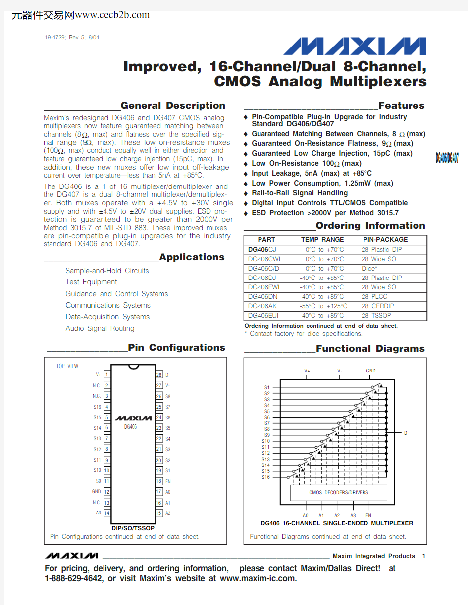
Maxim’s redesigned DG406 and DG407 CMOS analog multiplexers now feature guaranteed matching between channels (8?, max) and flatness over the specified sig-nal range (9?, max). These low on-resistance muxes (100?, max) conduct equally well in either direction and feature guaranteed low charge injection (15pC, max). In addition, these new muxes offer low input off-leakage current over temperature—less than 5nA at +85°C.
The DG406 is a 1 of 16 multiplexer/demultiplexer and the DG407 is a dual 8-channel multiplexer/demultiplex-er. Both muxes operate with a +4.5V to +30V single supply and with ±4.5V to ±20V dual supplies. ESD pro-tection is guaranteed to be greater than 2000V per Method 3015.7 of MIL-STD 883. These improved muxes are pin-compatible plug-in upgrades for the industry standard DG406 and DG407.
________________________Applications
Sample-and-Hold Circuits Test Equipment
Guidance and Control Systems Communications Systems Data-Acquisition Systems Audio Signal Routing
____________________________Features
?Pin-Compatible Plug-In Upgrade for Industry Standard DG406/DG407
?Guaranteed Matching Between Channels, 8?(max)?Guaranteed On-Resistance Flatness, 9?(max)?Guaranteed Low Charge Injection, 15pC (max)?Low On-Resistance 100?(max)?Input Leakage, 5nA (max) at +85°C
?Low Power Consumption, 1.25mW (max)?Rail-to-Rail Signal Handling
?Digital Input Controls TTL/CMOS Compatible ?ESD Protection >2000V per Method 3015.7
DG406/DG407
Improved, 16-Channel/Dual 8-Channel,
CMOS Analog Multiplexers
________________________________________________________________Maxim Integrated Products
1
_________________Pin Configurations
19-4729; Rev 5; 8/04
Ordering Information continued at end of data sheet.* Contact factory for dice specifications.
Ordering Information
_______________Functional Diagrams
For pricing, delivery, and ordering information,please contact Maxim/Dallas Direct!at 1-888-629-4642, or visit Maxim’s website at https://www.doczj.com/doc/8619133445.html,.
D G 406/D G 407
Improved, 16-Channel/Dual 8-Channel,CMOS Analog Multiplexers 2_______________________________________________________________________________________
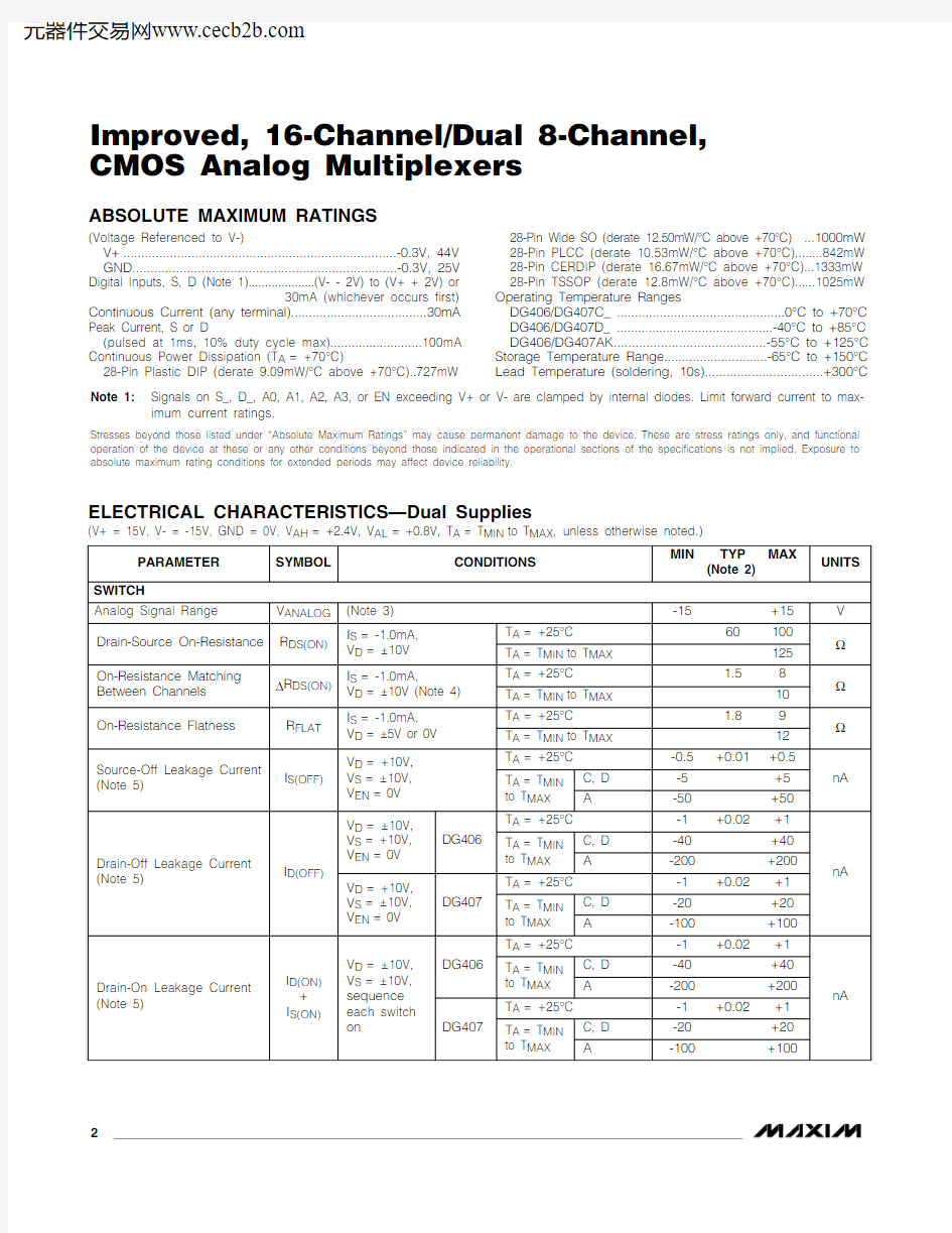
ABSOLUTE MAXIMUM RATINGS
ELECTRICAL CHARACTERISTICS—Dual Supplies
(V+ = 15V, V- = -15V, GND = 0V, V AH = +2.4V, V AL = +0.8V, T A = T MIN to T MAX , unless otherwise noted.)
Stresses beyond those listed under “Absolute Maximum Ratings” may cause permanent damage to the device. These are stress ratings only, and functional operation of the device at these or any other conditions beyond those indicated in the operational sections of the specifications is not implied. Exposure to absolute maximum rating conditions for extended periods may affect device reliability.
(Voltage Referenced to V-)
V+............................................................................-0.3V, 44V GND.........................................................................-0.3V, 25V Digital Inputs, S, D (Note 1)....................(V- - 2V) to (V+ + 2V) or
30mA (whichever occurs first)
Continuous Current (any terminal)......................................30mA Peak Current, S or D
(pulsed at 1ms, 10% duty cycle max)..........................100mA Continuous Power Dissipation (T A = +70°C)
28-Pin Plastic DIP (derate 9.09mW/°C above +70°C)..727mW 28-Pin Wide SO (derate 12.50mW/°C above +70°C)...1000mW 28-Pin PLCC (derate 10.53mW/°C above +70°C)........842mW 28-Pin CERDIP (derate 16.67mW/°C above +70°C)...1333mW 28-Pin TSSOP (derate 12.8mW/°C above +70°C)......1025mW Operating Temperature Ranges
DG406/DG407C_ ...............................................0°C to +70°C DG406/DG407D_ ............................................-40°C to +85°C DG406/DG407AK..........................................-55°C to +125°C Storage Temperature Range.............................-65°C to +150°C Lead Temperature (soldering, 10s).................................+300°C
Note 1:
Signals on S_, D_, A0, A1, A2, A3, or EN exceeding V+ or V- are clamped by internal diodes. Limit forward current to max-imum current ratings.
DG406/DG407
Improved, 16-Channel/Dual 8-Channel,
CMOS Analog Multiplexers
_______________________________________________________________________________________3
ELECTRICAL CHARACTERISTICS—Dual Supplies (continued)
(V+ = 15V, V- = -15V, GND = 0V, V AH = +2.4V, V AL = +0.8V, T A = T MIN to T MAX , unless otherwise noted.)
D G 406/D G 407
Improved, 16-Channel/Dual 8-Channel,CMOS Analog Multiplexers 4_______________________________________________________________________________________
ELECTRICAL CHARACTERISTICS—Single Supply
(V+ = 12V, V- = 0V, GND = 0V, V AH = +2.4V, V AL = +0.8V, T A = T MIN to T MAX , unless otherwise noted.)
Note 2:The algebraic convention where the most negative value is a minimum and the most positive value a maximum is used in
this data sheet.
Note 3:Guaranteed by design.
Note 4:?R ON = R ON(MAX)- R ON(MIN).On-resistance match between channels and flatness are guaranteed only with specified
voltages. Flatness is defined as the difference between the maximum and minimum value of on-resistance as measured at the extremes of the specified analog signal range.
Note 5:Leakage parameters are 100% tested at the maximum-rated hot temperature and guaranteed by correlation at +25°C.Note 6:Off-isolation = 20log V D /V S , where V D = output and V S = input to off switch.
DG406/DG407
Improved, 16-Channel/Dual 8-Channel,
CMOS Analog Multiplexers
_______________________________________________________________________________________5
120140
160ON-RESISTANCE vs. V D (DUAL SUPPLIES)
100
0204060-20
20-1515-10
10
-5
5
080V D (V)
r D S (O N ) (?)
120ON-RESISTANCE vs. V D
AND TEMPERATURE (DUAL SUPPLIES)
1000
204060-1515
-1010-55080V D (V)
r D S (O N ) (?)
280320
360
400
ON-RESISTANCE vs. V D (SINGLE SUPPLY)
24040
8012016015
20
105
200V D (V)
r D S (O N ) (?)
120140160
ON-RESISTANCE vs. V D AND TEMPERATURE (SINGLE SUPPLY)
10002040601510
5
80V D (V)
r D S (O N ) (?)
30CHARGE INJECTION vs. V D
20-30-20-100-15
15
-10
10
-5
5
010V D (V)
Q j (p C )
100.0001
-55125
OFF LEAKAGE vs. TEMPERATURE
1
TEMPERATURE (°C)
O F F L E A K A G E (n A )
250.010.001-35-15
65
0.11001000
45
851055
100.0001
-55125
ON LEAKAGE vs. TEMPERATURE
1TEMPERATURE (°C)
O N L E A K A G E (n A )
250.01
0.001-35-15
650.11001000
45851055
100
0.001
-55125
SUPPLY CURRENT vs. TEMPERATURE
10
TEMPERATURE (°C)
I +, I - (μA )
250.1
0.01
-35-15
65
1
45
851055
__________________________________________Typical Operating Characteristics
(T A = +25°C, unless otherwise noted.)
__________Applications Information
Operation with Supply Voltages
Other than ±15V
Using supply voltages other than ±15V reduces the analog signal range. The DG406/DG407 switches oper-ate with ±4.5V to ±20V bipolar supplies or with a +4.5V to +30V single supply; connect V- to GND when operat-ing with a single supply. Also, both device types can operate with unbalanced supplies such as +24V and -5V. The Typical Operating Characteristics graphs show typical on-resistance with 20V, 15V, 10V, and 5V supplies. (Switching times increase by a factor of two or more for operation at 5V.)
Overvoltage Protection
Proper power-supply sequencing is recommended for all CMOS devices. Do not exceed the absolute maxi-mum ratings because stresses beyond the listed rat-ings may cause permanent damage to the devices.Always sequence V+ on first, then V-, followed by the logic inputs and analog signals. If power-supply sequencing is not possible, add two small signal diodes in series with supply pins for overvoltage pro-tection (Figure 1). Adding diodes reduces the analog
signal range to 1V above V+ and 1V below V-, but low switch resistance and low leakage characteristics are unaffected. Device operation is unchanged, and the difference between V+ and V- should not exceed +44V.
D G 406/D G 407
Improved, 16-Channel/Dual 8-Channel,CMOS Analog Multiplexers 6_______________________________________________________________________________________
Bidirectional Output
D
28
Address Inputs A3–A014–17Enable Inputs
EN 18Bidirectional Analog Inputs S1–S819–26Negative Supply Voltage Input V-27Ground GND 12Bidirectional Analog Inputs S16–S94–11DG406PIN No Connection. Not internally connected.
N.C.2, 3, 13Positive Supply Voltage Input V+1FUNCTION
NAME
_____________________________________________________________Pin Descriptions
Diodes
DG406/DG407
Improved, 16-Channel/Dual 8-Channel,
CMOS Analog Multiplexers
_______________________________________________________________________________________
7
______________________________________________Test Circuits/Timing Diagrams
Figure 2. Transition Time
D G 406/D G 407
Improved, 16-Channel/Dual 8-Channel,CMOS Analog Multiplexers 8_______________________________________________________________________________________
_________________________________Test Circuits/Timing Diagrams (continued)
Figure 5. Charge Injection
DG406/DG407
Improved, 16-Channel/Dual 8-Channel,
CMOS Analog Multiplexers
_______________________________________________________________________________________9
_________________________________Test Circuits/Timing Diagrams (continued)
Figure 8. Source/Drain Capacitance
D G 406/D G 407
Improved, 16-Channel/Dual 8-Channel,CMOS Analog Multiplexers 10______________________________________________________________________________________
________Pin Configurations/Functional Diagrams/Truth Tables (continued)
A2A1A0EN ON Switch X 0000111100001111
X 0011001100110011
X 010101010101010101111111111111111
None 12345678910111213141516
DG406
LOGIC “0” V AL ≤ 0.8V, LOGIC “1” = V AH ≥ 2.4V
A3X 0000000011111111
A2
A1A0EN ON Switch X 00001111
X 00110011
X 01010101
011111111
None 12345678
DG407
LOGIC “0” V AL ≤ 0.8V, LOGIC “1” = V AH ≥ 2.4V
DG406/DG407
Improved, 16-Channel/Dual 8-Channel,
High-Performance, CMOS Analog Multiplexers
______________________________________________________________________________________11
_Ordering Information (continued)
* Contact factory for dice specifications.
__Functional Diagrams (continued)
D G 406/D G 407
Improved, 16-Channel/Dual 8-Channel,CMOS Analog Multiplexers 12______________________________________________________________________________________
__________________________________________________________Chip Topographies
GND
S1 S2 S3 S4 S5 S6 S7 S8
EN
A0
A1
A2
A3
N.C.
0.184"(4.67mm)0.078"(1.98mm)
S9S10S11S12S13S14S15S16N.C.
V-D V+
GND S1A S2A S3A S4A S5A S6A S7A S8A
EN
A0
A1
A2
N.C.N.C.
0.184"(4.67mm)0.078"(1.98mm)
S1B S2B S3B S4B S5B S6B S7B S8B DB
V-DA V+
DG406 TRANSISTOR COUNT: 269
SUBSTRATE IS INTERNALLY CONNECTED TO V+
DG407 TRANSISTOR COUNT: 269
SUBSTRATE IS INTERNALLY CONNECTED TO V+
DG406
DG407
N.C. = NO INTERNAL CONNECTION
DG406/DG407
Improved, 16-Channel/Dual 8-Channel,
High-Performance, CMOS Analog Multiplexers
Maxim cannot assume responsibility for use of any circuitry other than circuitry entirely embodied in a Maxim product. No circuit patent licenses are implied. Maxim reserves the right to change the circuitry and specifications without notice at any time.
Maxim Integrated Products, 120 San Gabriel Drive, Sunnyvale, CA 94086 408-737-7600 ____________________13?2004 Maxim Integrated Products
Printed USA
is a registered trademark of Maxim Integrated Products.
Package Information
(The package drawing(s) in this data sheet may not reflect the most current specifications. For the latest package outline information go to https://www.doczj.com/doc/8619133445.html,/packages .)