500 MHz, Triple 16 × 5
Video Crosspoint Switch
AD8177 Rev. 0
Information furnished by Analog Devices is believed to be accurate and reliable. However, no
responsibility is assumed by Analog Devices for its use, nor for any infringements of patents or other rights of third parties that may result from its use. Specifications subject to change without notice. No license is granted by implication or otherwise under any patent or patent rights of Analog Devices. T rademarks and registered trademarks are the property of their respective owners. One Technology Way, P.O. Box 9106, Norwood, MA 02062-9106, U.S.A. Tel: 781.329.4700 https://www.doczj.com/doc/9112110271.html, Fax: 781.461.3113 ?2007 Analog Devices, Inc. All rights reserved.
FEATURES
High channel count, triple 16 × 5 high speed, nonblocking switch array
Pin compatible with AD8175/AD8176 (16 × 9 switch arrays) and AD8178 (16 × 5 switch array)
Differential or single-ended operation
Supports sync-on common-mode and sync-on color operating modes
Decoded HV sync outputs available
G = +2 operation (differential input to differential output) Flexible power supplies: +5 V or ±2.5 V
Logic ground for convenient control interface
Serial or parallel programming of switch array
High impedance output disable allows connection of multiple devices with minimal loading on output bus Adjustable output CM and black level through external pins Excellent ac performance (to support 1600 × 1200 @ 85 Hz) Bandwidth: 500 MHz
Slew rate: 1800 V/μs
Settling time: 4 ns to 1%
Low power of 2.3 W
Low all-hostile crosstalk
?88 dB @ 5 MHz
?46 dB @ 500 MHz
Wide input common-mode range of 4 V
Reset pin allows disabling of all outputs
Fully populated 26 × 26 ball PBGA package
(27 mm × 27 mm, 1 mm ball pitch)
Convenient grouping of RGB signals for easy routing APPLICATIONS
RGB video switching
KVM
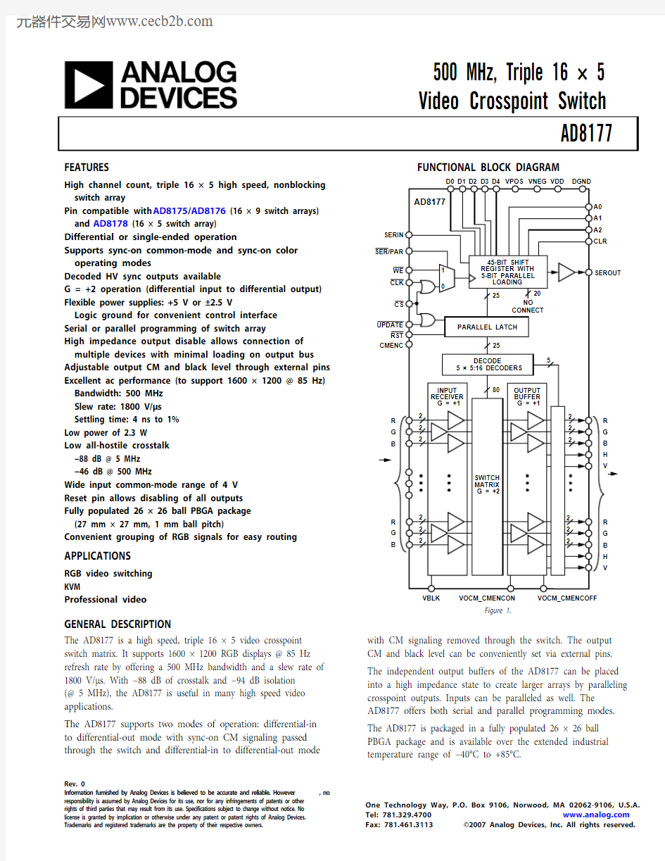
Professional video FUNCTIONAL BLOCK DIAGRAM
VBLK VOCM_CMENCON VOCM_CMENCOFF
5
x
R
G
B
,
H
C
H
A
N
N
E
L
6
6
5
-
1
Figure 1.
GENERAL DESCRIPTION
The AD8177 is a high speed, triple 16 × 5 video crosspoint switch matrix. It supports 1600 × 1200 RGB displays @ 85 Hz refresh rate by offering a 500 MHz bandwidth and a slew rate of 1800 V/μs. With ?88 dB of crosstalk and ?94 dB isolation (@ 5 MHz), the AD8177 is useful in many high speed video applications.
The AD8177 supports two modes of operation: differential-in to differential-out mode with sync-on CM signaling passed through the switch and differential-in to differential-out mode with CM signaling removed through the switch. The output CM and black level can be conveniently set via external pins. The independent output buffers of the AD8177 can be placed into a high impedance state to create larger arrays by paralleling crosspoint outputs. Inputs can be paralleled as well. The
AD8177 offers both serial and parallel programming modes. The AD8177 is packaged in a fully populated 26 × 26 ball PBGA package and is available over the extended industrial temperature range of ?40°C to +85°C.
AD8177
Rev. 0 | Page 2 of 40
TABLE OF CONTENTS
Features..............................................................................................1 Applications.......................................................................................1 Functional Block Diagram..............................................................1 General Description.........................................................................1 Revision History...............................................................................2 Specifications.....................................................................................3 Timing Characteristics (Serial Mode).......................................5 Timing Characteristics (Parallel Mode)....................................6 Absolute Maximum Ratings............................................................7 Thermal Resistance......................................................................7 Power Dissipation.........................................................................7 ESD Caution..................................................................................7 Pin Configuration and Function Descriptions..............................8 Truth Table and Logic Diagram...............................................17 Equivalent Circuits.........................................................................19 Typical Performance Characteristics...........................................21 Theory of Operation......................................................................26 Applications Information..............................................................27 Operating Modes........................................................................27 Programming..............................................................................28 Differential and Single-Ended Operation...............................30 Outline Dimensions.......................................................................39 Ordering Guide.. (39)
REVISION HISTORY
7/07—Revision 0: Initial Version
AD8177
Rev. 0 | Page 3 of 40
SPECIFICATIONS
V S = ±2.5 V at T A = 25°C, G = +2, R L = 100 Ω (each output), VBLK = 0 V , output CM voltage = 0 V , differential I/O mode, unless otherwise noted. Table 1.
Parameter Conditions Min Typ Max Unit DYNAMIC PERFORMANCE ?3 dB Bandwidth 200 mV p-p 500 MHz 2 V p-p 450 MHz Gain Flatness 0.1 dB, 200 mV p-p 25 MHz Propagation Delay 2 V p-p 1.3 ns Settling Time 1%, 2 V step 4 ns Slew Rate, Differential Output 2 V step 1800 V/μs 2 V step, 10% to 90% 1500 V/μs Slew Rate, RGB Common Mode 1 V step, 10% to 90% 300 V/μs Slew Rate, HV Outputs Rail-to-rail, TTL load 400 V/μs NOISE/DISTORTION PERFORMANCE Crosstalk, All Hostile f = 5 MHz ?88 dB f = 10 MHz ?82 dB f = 100 MHz ?58 dB f = 500 MHz ?46 dB Off Isolation, Input to Output f = 5 MHz, R L = 100 Ω, one channel ?94 dB Input Voltage Noise 0.01 MHz to 100 MHz 40 nV/√Hz DC PERFORMANCE Gain Error 1 % Gain Matching R, G, B same channel 0.5 % Gain Temperature Coefficient 40 ppm/°C OUTPUT CHARACTERISTICS Output Offset Voltage CMENC on or off 10 mV Temperature coefficient 31 μV/°C
Output Offset Voltage,
RGB Common Mode
CMENC on or off 10 mV Temperature coefficient ?7.6 μV/°C Output Impedance Enabled, differential 1.5 Ω Disabled, differential 2.7 kΩ Output Disable Capacitance Disabled 2 pF Output Leakage Current Disabled 1 μA Output Voltage Range No load, differential 4 V p-p Output Current Short circuit 45 mA INPUT CHARACTERISTICS
Input Voltage Range,
Differential Mode
2 V p-p Input Voltage Range,
Common Mode V IN = 1 V p-p, differential ±2.25 V CMR, RGB Input ΔV OUT, DM /ΔV IN, CM , ΔV IN, CM = ±0.5 V, CMENC off –62 dB ΔV OUT, DM /ΔV IN, CM , ΔV IN, CM = ±0.5 V, CMENC on ?45 dB CM Gain, RGB Input ΔV OUT, CM /ΔV IN, CM , ΔV IN, CM = ±0.5 V CMENC off ?70 dB ΔV OUT, CM /ΔV IN, CM , ΔV IN, CM = ±0.5 V, CMENC on 0 dB Input Capacitance Any switch configuration 2 pF Input Resistance Differential 3.33 kΩ Input Offset Current 1 μA
AD8177
Rev. 0 | Page 4 of 40
AD8177
Rev. 0 | Page 5 of 40
TIMING CHARACTERISTICS (SERIAL MODE)
06605-002
Figure 2. Timing Diagram, Serial Mode
Table 4. H and V Logic Levels, V DD = 3.3 V
V OH
V OL
I OH
I OL
2.7 V min
0.5 V max
–3 mA max
3 mA max
Table 5. RST Logic Levels, V DD = 3.3 V
V IH
V IL
I IH
I IL
2.0 V min
0.6 V max
?60 μA max
?120 μA max
Table 6. CS Logic Levels, V DD = 3.3 V
V OH
V OL
I IH
I OL
2.0 V min
0.6 V max
100 μA max
40 μA max
AD8177
Rev. 0 | Page 6 of 40
TIMING CHARACTERISTICS (PARALLEL MODE)
06605-003
Figure 3. Timing Diagram, Parallel Mode
Table 9. H and V Logic Levels, V DD = 3.3 V
V OH
V OL
I OH
I OL
2.7 V min
0.5 V max
–3 mA max
3 mA max
Table 10. RST Logic Levels, V DD = 3.3 V
V IH
V IL
I IH
I IL
2.0 V min
0.6 V max
?60 μA max
?120 μA max
Table 11. CS Logic Levels, V DD = 3.3 V
V OH
V OL
I IH
I OL
2.0 V min
0.6 V max
100 μA max
40 μA max
AD8177
Rev. 0 | Page 7 of 40
ABSOLUTE MAXIMUM RATINGS
Table 12.
Parameter Rating Analog Supply Voltage (V POS – V NEG ) 6 V Digital Supply Voltage (V DD – D GND ) 6 V Ground Potential Difference (V NEG – D GND )
+0.5 V to ?2.5 V Maximum Potential Difference
(V DD – V NEG )
8 V Common-Mode Analog Input Voltage (V NEG – 0.5 V)
to (V POS + 0.5 V) Differential Analog Input Voltage ±2 V Digital Input Voltage V DD Output Voltage (Disabled Analog Output) (V POS – 1 V) to (V NEG + 1 V) Output Short-Circuit Duration Momentary Storage Temperature Range ?65°C to +125°C Operating Temperature Range ?40°C to +85°C Lead Temperature (Soldering, 10 sec) 300°C Junction Temperature 150°C Stresses above those listed under Absolute Maximum Ratings may cause permanent damage to the device. This is a stress rating only; functional operation of the device at these or any other conditions above those indicated in the operational
section of this specification is not implied. Exposure to absolute maximum rating conditions for extended periods may affect device reliability.
THERMAL RESISTANCE
θJA is specified for the worst-case conditions, that is, a device soldered in a circuit board for surface-mount packages.
Table 13. Thermal Resistance
Package Type θJA Unit PBGA 15 °C/W
POWER DISSIPATION
The AD8177 is operated with ±2.5 V or +5 V supplies and can drive loads down to 100 Ω, resulting in a large range of possible power dissipations. For this reason, extra care must be taken
derating the operating conditions based on ambient temperature.
Packaged in a 676-lead PBGA the AD8177 junction-to-ambient thermal impedance (θJA ) is 15°C/W . For long-term reliability, the maximum allowed junction temperature of the die should not exceed 150°C. Temporarily exceeding this limit may cause
a shift in parametric performance due to a change in stresses exerted on the die by the package. Exceeding a junction
temperature of 175°C for an extended period can result in
device failure. The following curve shows the range of allowed internal die power dissipations that meet these conditions over the ?40°C to +85°C ambient temperature range. When using Table 13, do not include external load power in the maximum power calculation, but do include load current dropped on the die output transistors.
06605-004
AMBIENT TEMPERATURE (°C)M A X I M U M P O W E R (W )
345678910
15
25354555657585
Figure 4. Maximum Die Power Dissipation vs. Ambient Temperature
ESD CAUTION
AD8177
Rev. 0 | Page 8 of 40
PIN CONFIGURATION AND FUNCTION DESCRIPTIONS
A A
B B
C C
D D
E E
F F
G G
H H J J K K L L M M N N P P R R T T U U V V W W Y Y AA AA AB AB AC AC AD AD AE AE
AF
AF
2625242322212019181716151413121110
987654321
06605-005
Figure 5. Pin Configuration, Package Bottom View
AD8177
Rev. 0 | Page 9 of 40
A A
B B
C C
D D
E E
F F
G G
H H J J K K L L M M N N P P R R T T U U V V W W Y Y AA AA AB AB AC AC AD AD AE AE
AF
AF
123456789101112131415161718
1920212223242526
06605-006
Figure 6. Pin Configuration, Package Top View
AD8177
Rev. 0 | Page 10 of 40
Table 14. Ball Grid Function Descriptions
Ball No. Mnemonic Description
A1 VNEG Negative Analog Power Supply. A2 VNEG Negative Analog Power Supply. A3 VNEG Negative Analog Power Supply. A4 INB12 Input Number 12, Negative Phase. A5 IPR12 Input Number 12, Positive Phase. A6 VPOS Positive Analog Power Supply. A7 INB11 Input Number 11, Negative Phase. A8 IPR11 Input Number 11, Positive Phase. A9 VNEG Negative Analog Power Supply. A10 INB10 Input Number 10, Negative Phase. A11 IPR10 Input Number 10, Positive Phase. A12 VPOS Positive Analog Power Supply. A13 INB9 Input Number 9, Negative Phase. A14 IPR9 Input Number 9, Positive Phase. A15 VNEG Negative Analog Power Supply. A16 INB8 Input Number 8, Negative Phase. A17 IPR8 Input Number 8, Positive Phase. A18 VPOS Positive Analog Power Supply. A19 ONB4 Output Number 4, Negative Phase. A20 OPR4 Output Number 4, Positive Phase. A21 VNEG Negative Analog Power Supply. A22 NC No Connect. A23 NC No Connect.
A24 VNEG Negative Analog Power Supply. A25 VNEG Negative Analog Power Supply. A26 VNEG Negative Analog Power Supply. B1 VNEG Negative Analog Power Supply. B2 VNEG Negative Analog Power Supply. B3 VNEG Negative Analog Power Supply. B4 IPB12 Input Number 12, Positive Phase. B5 INR12 Input Number 12, Negative Phase. B6 VPOS Positive Analog Power Supply. B7 IPB11 Input Number 11, Positive Phase. B8 INR11 Input Number 11, Negative Phase. B9 VNEG Negative Analog Power Supply. B10 IPB10 Input Number 10, Positive Phase. B11 INR10 Input Number 10, Negative Phase. B12 VPOS Positive Analog Power Supply. B13 IPB9 Input Number 9, Positive Phase. B14 INR9 Input Number 9, Negative Phase. B15 VNEG Negative Analog Power Supply. B16 IPB8 Input Number 8, Positive Phase. B17 INR8 Input Number 8, Negative Phase. B18 VPOS Positive Analog Power Supply. B19 OPB4 Output Number 4, Positive Phase. B20 ONR4 Output Number 4, Negative Phase. B21 VNEG Negative Analog Power Supply. B22 NC No Connect. B23 NC No Connect.
B24 VNEG Negative Analog Power Supply. B25 VNEG
Negative Analog Power Supply.
Ball No. Mnemonic Description
B26 VNEG Negative Analog Power Supply. C1 VNEG Negative Analog Power Supply. C2 VNEG Negative Analog Power Supply. C3 VNEG Negative Analog Power Supply. C4 ING12 Input Number 12, Negative Phase. C5 IPG12 Input Number 12, Positive Phase. C6 VPOS Positive Analog Power Supply. C7 ING11 Input Number 11, Negative Phase. C8 IPG11 Input Number 11, Positive Phase. C9 VNEG Negative Analog Power Supply. C10 ING10 Input Number 10, Negative Phase. C11 IPG10 Input Number 10, Positive Phase. C12 VPOS Positive Analog Power Supply. C13 ING9 Input Number 9, Negative Phase. C14 IPG9 Input Number 9, Positive Phase. C15 VNEG Negative Analog Power Supply. C16 ING8 Input Number 8, Negative Phase. C17 IPG8 Input Number 8, Positive Phase. C18 VPOS Positive Analog Power Supply. C19 ONG4 Output Number 4, Negative Phase. C20 OPG4 Output Number 4, Positive Phase. C21 VNEG Negative Analog Power Supply. C22 NC No Connect. C23 NC No Connect.
C24 VNEG Negative Analog Power Supply. C25 VNEG Negative Analog Power Supply. C26 VNEG Negative Analog Power Supply. D1 IPR13 Input Number 13, Positive Phase. D2 INR13 Input Number 13, Negative Phase. D3 IPG13 Input Number 13, Positive Phase. D4 VPOS Positive Analog Power Supply. D5 VPOS Positive Analog Power Supply. D6 VPOS Positive Analog Power Supply. D7 VPOS Positive Analog Power Supply. D8 VPOS Positive Analog Power Supply. D9 VPOS Positive Analog Power Supply. D10 VPOS Positive Analog Power Supply. D11 VPOS Positive Analog Power Supply. D12 VPOS Positive Analog Power Supply. D13 VPOS Positive Analog Power Supply. D14 VPOS Positive Analog Power Supply. D15 VPOS Positive Analog Power Supply. D16 VPOS Positive Analog Power Supply. D17 VPOS Positive Analog Power Supply. D18 VPOS Positive Analog Power Supply. D19 V4 Output Number 4, V Sync. D20 H4 Output Number 4, H Sync. D21 VPOS Positive Analog Power Supply. D22 NC No Connect. D23 NC No Connect.
D24 VNEG
Negative Analog Power Supply.
AD8177
Rev. 0 | Page 11 of 40
Ball No. Mnemonic Description
F25 VPOS Positive Analog Power Supply. F26 VPOS Positive Analog Power Supply. G1 VPOS Positive Analog Power Supply. G2 VPOS Positive Analog Power Supply. G3 VPOS Positive Analog Power Supply. G4 VPOS Positive Analog Power Supply. G5 VPOS Positive Analog Power Supply. G6 VPOS Positive Analog Power Supply. G7 VPOS Positive Analog Power Supply. G8 VPOS Positive Analog Power Supply. G9 VPOS Positive Analog Power Supply. G10 VPOS Positive Analog Power Supply. G11 VPOS Positive Analog Power Supply. G12 VPOS Positive Analog Power Supply. G13 VPOS Positive Analog Power Supply. G14 VPOS Positive Analog Power Supply. G15 VPOS Positive Analog Power Supply. G16 VPOS Positive Analog Power Supply. G17 VPOS Positive Analog Power Supply. G18 VPOS Positive Analog Power Supply. G19 VPOS Positive Analog Power Supply. G20 VPOS Positive Analog Power Supply. G21 VPOS Positive Analog Power Supply. G22 VPOS Positive Analog Power Supply. G23 V3 Output Number 3, V Sync.
G24 ONG3 Output Number 3, Negative Phase. G25 OPB3 Output Number 3, Positive Phase. G26 ONB3 Output Number 3, Negative Phase. H1 IPR14 Input Number 14, Positive Phase. H2 INR14 Input Number 14, Negative Phase. H3 IPG14 Input Number 14, Positive Phase. H4 VPOS Positive Analog Power Supply. H5 VPOS Positive Analog Power Supply. H6 VPOS Positive Analog Power Supply. H7 VPOS Positive Analog Power Supply. H8 VNEG Negative Analog Power Supply. H9 VNEG Negative Analog Power Supply. H10 VNEG Negative Analog Power Supply. H11 VNEG Negative Analog Power Supply. H12 VNEG Negative Analog Power Supply. H13 VNEG Negative Analog Power Supply. H14 VNEG Negative Analog Power Supply. H15 VNEG Negative Analog Power Supply. H16 VNEG Negative Analog Power Supply. H17 VNEG Negative Analog Power Supply. H18 VNEG Negative Analog Power Supply. H19 VNEG Negative Analog Power Supply. H20 VNEG Negative Analog Power Supply. H21 VPOS Positive Analog Power Supply. H22 VPOS Positive Analog Power Supply. H23 H3 Output Number 3, H Sync.
H24
OPG3
Output Number 3, Positive Phase.
AD8177
Rev. 0 | Page 12 of 40
Ball No. Mnemonic Description
H25 ONR3 Output Number 3, Negative Phase. H26 OPR3 Output Number 3, Positive Phase. J1 INB14 Input Number 14, Negative Phase. J2 IPB14 Input Number 14, Positive Phase. J3 ING14 Input Number 14, Negative Phase. J4 VPOS Positive Analog Power Supply. J5 VPOS Positive Analog Power Supply. J6 VPOS Positive Analog Power Supply. J7 VPOS Positive Analog Power Supply. J8 VNEG Negative Analog Power Supply. J9 VNEG Negative Analog Power Supply. J10 VNEG Negative Analog Power Supply. J11 VNEG Negative Analog Power Supply. J12 VNEG Negative Analog Power Supply. J13 VNEG Negative Analog Power Supply. J14 VNEG Negative Analog Power Supply. J15 VNEG Negative Analog Power Supply. J16 VNEG Negative Analog Power Supply. J17 VNEG Negative Analog Power Supply. J18 VNEG Negative Analog Power Supply. J19 VNEG Negative Analog Power Supply. J20 VNEG Negative Analog Power Supply. J21 VPOS Positive Analog Power Supply. J22 VPOS Positive Analog Power Supply. J23 VPOS Positive Analog Power Supply. J24 VNEG Negative Analog Power Supply. J25 VNEG Negative Analog Power Supply. J26 VNEG Negative Analog Power Supply. K1 VNEG Negative Analog Power Supply. K2 VNEG Negative Analog Power Supply. K3 VNEG Negative Analog Power Supply. K4 VPOS Positive Analog Power Supply. K5 VPOS Positive Analog Power Supply. K6 VPOS Positive Analog Power Supply. K7 VPOS Positive Analog Power Supply. K8 VNEG Negative Analog Power Supply. K9 VNEG Negative Analog Power Supply. K10 VNEG Negative Analog Power Supply. K11 VNEG Negative Analog Power Supply. K12 VNEG Negative Analog Power Supply. K13 VNEG Negative Analog Power Supply. K14 VNEG Negative Analog Power Supply. K15 VNEG Negative Analog Power Supply. K16 VNEG Negative Analog Power Supply. K17 VNEG Negative Analog Power Supply. K18 VNEG Negative Analog Power Supply. K19 VNEG Negative Analog Power Supply. K20 VNEG Negative Analog Power Supply. K21 VPOS Positive Analog Power Supply. K22 VPOS Positive Analog Power Supply. K23 NC No Connect. K24 NC No Connect. Ball No. Mnemonic
Description
K25 NC No Connect. K26 NC No Connect.
L1 IPR15 Input Number 15, Positive Phase. L2 INR15 Input Number 15, Negative Phase. L3 IPG15 Input Number 15, Positive Phase. L4 VPOS Positive Analog Power Supply. L5 VPOS Positive Analog Power Supply. L6 VPOS Positive Analog Power Supply. L7 VPOS Positive Analog Power Supply. L8 VNEG Negative Analog Power Supply. L9 VNEG Negative Analog Power Supply. L10 VNEG Negative Analog Power Supply. L11 VNEG Negative Analog Power Supply. L12 VNEG Negative Analog Power Supply. L13 VNEG Negative Analog Power Supply. L14 VNEG Negative Analog Power Supply. L15 VNEG Negative Analog Power Supply. L16 VNEG Negative Analog Power Supply. L17 VNEG Negative Analog Power Supply. L18 VNEG Negative Analog Power Supply. L19 VNEG Negative Analog Power Supply. L20 VNEG Negative Analog Power Supply. L21 VPOS Positive Analog Power Supply. L22 VPOS Positive Analog Power Supply. L23 NC No Connect. L24 NC No Connect. L25 NC No Connect. L26 NC No Connect.
M1 INB15 Input Number 15, Negative Phase. M2 IPB15 Input Number 15, Positive Phase. M3 ING15 Input Number 15, Negative Phase. M4 VPOS Positive Analog Power Supply. M5 VPOS Positive Analog Power Supply. M6 VPOS Positive Analog Power Supply. M7 VPOS Positive Analog Power Supply. M8 VNEG Negative Analog Power Supply. M9 VNEG Negative Analog Power Supply. M10 VNEG Negative Analog Power Supply. M11 VNEG Negative Analog Power Supply. M12 VNEG Negative Analog Power Supply. M13 VNEG Negative Analog Power Supply. M14 VNEG Negative Analog Power Supply. M15 VNEG Negative Analog Power Supply. M16 VNEG Negative Analog Power Supply. M17 VNEG Negative Analog Power Supply. M18 VNEG Negative Analog Power Supply. M19 VNEG Negative Analog Power Supply. M20 VNEG Negative Analog Power Supply. M21 VPOS Positive Analog Power Supply. M22 VPOS Positive Analog Power Supply. M23 VPOS Positive Analog Power Supply. M24 VPOS Positive Analog Power Supply.
AD8177
Rev. 0 | Page 13 of 40
Ball No.
Mnemonic Description
M25 VPOS Positive Analog Power Supply. M26 VPOS Positive Analog Power Supply. N1 VPOS Positive Analog Power Supply. N2 VPOS Positive Analog Power Supply. N3 VPOS Positive Analog Power Supply. N4 VPOS Positive Analog Power Supply. N5 VOCM_ CMENCON Output CM Reference with CM Encoding On.
N6 VPOS Positive Analog Power Supply. N7 VPOS Positive Analog Power Supply. N8 VNEG Negative Analog Power Supply. N9 VNEG Negative Analog Power Supply. N10 VNEG Negative Analog Power Supply. N11 VNEG Negative Analog Power Supply. N12 VNEG Negative Analog Power Supply. N13 VNEG Negative Analog Power Supply. N14 VNEG Negative Analog Power Supply. N15 VNEG Negative Analog Power Supply. N16 VNEG Negative Analog Power Supply. N17 VNEG Negative Analog Power Supply. N18 VNEG Negative Analog Power Supply. N19 VNEG Negative Analog Power Supply. N20 VNEG Negative Analog Power Supply. N21 VPOS Positive Analog Power Supply. N22 VPOS Positive Analog Power Supply. N23 V2 Output Number 2, V Sync.
N24 ONG2 Output Number 2, Negative Phase. N25 OPB2 Output Number 2, Positive Phase. N26 ONB2 Output Number 2, Negative Phase. P1 VPOS Positive Analog Power Supply. P2 VPOS Positive Analog Power Supply. P3 VPOS Positive Analog Power Supply. P4 VPOS Positive Analog Power Supply. P5 VBLK Output Blank Level.
P6 VPOS Positive Analog Power Supply. P7 VPOS Positive Analog Power Supply. P8 VNEG Negative Analog Power Supply. P9 VNEG Negative Analog Power Supply. P10 VNEG Negative Analog Power Supply. P11 VNEG Negative Analog Power Supply. P12 VNEG Negative Analog Power Supply. P13 VNEG Negative Analog Power Supply. P14 VNEG Negative Analog Power Supply. P15 VNEG Negative Analog Power Supply. P16 VNEG Negative Analog Power Supply. P17 VNEG Negative Analog Power Supply. P18 VNEG Negative Analog Power Supply. P19 VNEG Negative Analog Power Supply. P20 VNEG Negative Analog Power Supply. P21 VPOS Positive Analog Power Supply. P22 VPOS Positive Analog Power Supply. P23 H2 Output Number 2, H Sync.
P24
OPG2
Output Number 2, Positive Phase.
Ball No. Mnemonic Description
P25 ONR2 Output Number 2, Negative Phase. P26 OPR2 Output Number 2, Positive Phase. R1 IPR7 Input Number 7, Positive Phase. R2 INR7 Input Number 7, Negative Phase. R3 IPG7 Input Number 7, Positive Phase. R4 VPOS Positive Analog Power Supply. R5
VOCM_ CMENCOFF
Output Reference with CM Encoding Off.
R6 VPOS Positive Analog Power Supply. R7 VPOS Positive Analog Power Supply. R8 VNEG Negative Analog Power Supply. R9 VNEG Negative Analog Power Supply. R10 VNEG Negative Analog Power Supply. R11 VNEG Negative Analog Power Supply. R12 VNEG Negative Analog Power Supply. R13 VNEG Negative Analog Power Supply. R14 VNEG Negative Analog Power Supply. R15 VNEG Negative Analog Power Supply. R16 VNEG Negative Analog Power Supply. R17 VNEG Negative Analog Power Supply. R18 VNEG Negative Analog Power Supply. R19 VNEG Negative Analog Power Supply. R20 VNEG Negative Analog Power Supply. R21 VPOS Positive Analog Power Supply. R22 VPOS Positive Analog Power Supply. R23 VPOS Positive Analog Power Supply. R24 VNEG Negative Analog Power Supply. R25 VNEG Negative Analog Power Supply. R26 VNEG Negative Analog Power Supply. T1 INB7 Input Number 7, Negative Phase. T2 IPB7 Input Number 7, Positive Phase. T3 ING7 Input Number 7, Negative Phase. T4 VPOS Positive Analog Power Supply. T5 VPOS Positive Analog Power Supply. T6 VPOS Positive Analog Power Supply. T7 VPOS Positive Analog Power Supply. T8 VNEG Negative Analog Power Supply. T9 VNEG Negative Analog Power Supply. T10 VNEG Negative Analog Power Supply. T11 VNEG Negative Analog Power Supply. T12 VNEG Negative Analog Power Supply. T13 VNEG Negative Analog Power Supply. T14 VNEG Negative Analog Power Supply. T15 VNEG Negative Analog Power Supply. T16 VNEG Negative Analog Power Supply. T17 VNEG Negative Analog Power Supply. T18 VNEG Negative Analog Power Supply. T19 VNEG Negative Analog Power Supply. T20 VNEG Negative Analog Power Supply. T21 VPOS Positive Analog Power Supply. T22 VPOS Positive Analog Power Supply. T23 NC No Connect. T24 NC
No Connect.
AD8177
Rev. 0 | Page 14 of 40
Ball No. Mnemonic Description
T25 NC No Connect. T26 NC No Connect.
U1 VNEG Negative Analog Power Supply. U2 VNEG Negative Analog Power Supply. U3 VNEG Negative Analog Power Supply. U4 VPOS Positive Analog Power Supply. U5 VPOS Positive Analog Power Supply. U6 VPOS Positive Analog Power Supply. U7 VPOS Positive Analog Power Supply. U8 VNEG Negative Analog Power Supply. U9 VNEG Negative Analog Power Supply. U10 VNEG Negative Analog Power Supply. U11 VNEG Negative Analog Power Supply. U12 VNEG Negative Analog Power Supply. U13 VNEG Negative Analog Power Supply. U14 VNEG Negative Analog Power Supply. U15 VNEG Negative Analog Power Supply. U16 VNEG Negative Analog Power Supply. U17 VNEG Negative Analog Power Supply. U18 VNEG Negative Analog Power Supply. U19 VNEG Negative Analog Power Supply. U20 VNEG Negative Analog Power Supply. U21 VPOS Positive Analog Power Supply. U22 VPOS Positive Analog Power Supply. U23 NC No Connect. U24 NC No Connect. U25 NC No Connect. U26 NC No Connect.
V1 IPR6 Input Number 6, Positive Phase. V2 INR6 Input Number 6, Negative Phase. V3 IPG6 Input Number 6, Positive Phase. V4 VPOS Positive Analog Power Supply. V5 VPOS Positive Analog Power Supply. V6 VPOS Positive Analog Power Supply. V7 VPOS Positive Analog Power Supply. V8 VNEG Negative Analog Power Supply. V9 VNEG Negative Analog Power Supply. V10 VNEG Negative Analog Power Supply. V11 VNEG Negative Analog Power Supply. V12 VNEG Negative Analog Power Supply. V13 VNEG Negative Analog Power Supply. V14 VNEG Negative Analog Power Supply. V15 VNEG Negative Analog Power Supply. V16 VNEG Negative Analog Power Supply. V17 VNEG Negative Analog Power Supply. V18 VNEG Negative Analog Power Supply. V19 VNEG Negative Analog Power Supply. V20 VNEG Negative Analog Power Supply. V21 VPOS Positive Analog Power Supply. V22 VPOS Positive Analog Power Supply. V23 VPOS Positive Analog Power Supply. V24 VPOS Positive Analog Power Supply. Ball No. Mnemonic Description
V25 VPOS Positive Analog Power Supply. V26 VPOS Positive Analog Power Supply. W1 INB6 Input Number 6, Negative Phase. W2 IPB6 Input Number 6, Positive Phase. W3 ING6 Input Number 6, Negative Phase. W4 VPOS Positive Analog Power Supply. W5 VPOS Positive Analog Power Supply. W6 VPOS Positive Analog Power Supply. W7 VPOS Positive Analog Power Supply. W8 VNEG Negative Analog Power Supply. W9 VNEG Negative Analog Power Supply. W10 VNEG Negative Analog Power Supply. W11 VNEG Negative Analog Power Supply. W12 VNEG Negative Analog Power Supply. W13 VNEG Negative Analog Power Supply. W14 VNEG Negative Analog Power Supply. W15 VNEG Negative Analog Power Supply. W16 VNEG Negative Analog Power Supply. W17 VNEG Negative Analog Power Supply. W18 VNEG Negative Analog Power Supply. W19 VNEG Negative Analog Power Supply. W20 VNEG Negative Analog Power Supply. W21 VPOS Positive Analog Power Supply. W22 VPOS Positive Analog Power Supply. W23 V1 Output Number 1, V Sync.
W24 ONG1 Output Number 1, Negative Phase. W25 OPB1 Output Number 1, Positive Phase. W26 ONB1 Output Number 1, Negative Phase. Y1 VPOS Positive Analog Power Supply. Y2 VPOS Positive Analog Power Supply. Y3 VPOS Positive Analog Power Supply. Y4 VPOS Positive Analog Power Supply. Y5 VPOS Positive Analog Power Supply. Y6 VPOS Positive Analog Power Supply. Y7 VPOS Positive Analog Power Supply. Y8 VPOS Positive Analog Power Supply. Y9 VPOS Positive Analog Power Supply. Y10 VPOS Positive Analog Power Supply. Y11 VPOS Positive Analog Power Supply. Y12 VPOS Positive Analog Power Supply. Y13 VPOS Positive Analog Power Supply. Y14 VPOS Positive Analog Power Supply. Y15 VPOS Positive Analog Power Supply. Y16 VPOS Positive Analog Power Supply. Y17 VPOS Positive Analog Power Supply. Y18 VPOS Positive Analog Power Supply. Y19 VPOS Positive Analog Power Supply. Y20 VPOS Positive Analog Power Supply. Y21 VPOS Positive Analog Power Supply. Y22 VPOS Positive Analog Power Supply. Y23 H1 Output Number 1, H Sync.
Y24 OPG1 Output Number 1, Positive Phase.
AD8177
Rev. 0 | Page 15 of 40
Ball No. Mnemonic Description
AB25 VNEG Negative Analog Power Supply. AB26 VNEG Negative Analog Power Supply. AC1 INB5 Input Number 5, Negative Phase. AC2 IPB5 Input Number 5, Positive Phase. AC3 ING5 Input Number 5, Negative Phase. AC4 VPOS Positive Analog Power Supply. AC5 VPOS Positive Analog Power Supply. AC6 VPOS Positive Analog Power Supply. AC7 VPOS Positive Analog Power Supply. AC8 VPOS Positive Analog Power Supply. AC9 VPOS Positive Analog Power Supply. AC10 VPOS Positive Analog Power Supply. AC11 VPOS Positive Analog Power Supply. AC12 VPOS Positive Analog Power Supply. AC13 VPOS Positive Analog Power Supply. AC14 VPOS Positive Analog Power Supply. AC15 VPOS Positive Analog Power Supply. AC16 VPOS Positive Analog Power Supply. AC17 VPOS Positive Analog Power Supply. AC18 VPOS Positive Analog Power Supply. AC19 H0 Output Number 0, H Sync. AC20 V0 Output Number 0, V Sync. AC21 VPOS Positive Analog Power Supply. AC22 NC No Connect. AC23 NC No Connect.
AC24 VNEG Negative Analog Power Supply. AC25 VNEG Negative Analog Power Supply. AC26 VNEG Negative Analog Power Supply. AD1 VNEG Negative Analog Power Supply. AD2 VNEG Negative Analog Power Supply. AD3 VNEG Negative Analog Power Supply. AD4 IPG4 Input Number 4, Positive Phase. AD5 ING4 Input Number 4, Negative Phase. AD6 VNEG Negative Analog Power Supply. AD7 IPG3 Input Number 3, Positive Phase. AD8 ING3 Input Number 3, Negative Phase. AD9 VPOS Positive Analog Power Supply. AD10 IPG2 Input Number 2, Positive Phase. AD11 ING2 Input Number 2, Negative Phase. AD12 VNEG Negative Analog Power Supply. AD13 IPG1 Input Number 1, Positive Phase. AD14 ING1 Input Number 1, Negative Phase. AD15 VPOS Positive Analog Power Supply. AD16 IPG0 Input Number 0, Positive Phase. AD17 ING0 Input Number 0, Negative Phase. AD18 VNEG Negative Analog Power Supply. AD19 OPG0 Output Number 0, Positive Phase. AD20 ONG0 Output Number 0, Negative Phase. AD21 VPOS Positive Analog Power Supply. AD22 NC No Connect. AD23 NC No Connect.
AD24 VNEG
Negative Analog Power Supply.
AD8177
Rev. 0 | Page 16 of 40
Ball No. Mnemonic Description
AD25 VNEG Negative Analog Power Supply. AD26 VNEG Negative Analog Power Supply. AE1 VNEG Negative Analog Power Supply. AE2 VNEG Negative Analog Power Supply. AE3 VNEG Negative Analog Power Supply. AE4 INR4 Input Number 4, Negative Phase. AE5 IPB4 Input Number 4, Positive Phase. AE6 VNEG Negative Analog Power Supply. AE7 INR3 Input Number 3, Negative Phase. AE8 IPB3 Input Number 3, Positive Phase. AE9 VPOS Positive Analog Power Supply. AE10 INR2 Input Number 2, Negative Phase. AE11 IPB2 Input Number 2, Positive Phase. AE12 VNEG Negative Analog Power Supply. AE13 INR1 Input Number 1, Negative Phase. AE14 IPB1 Input Number 1, Positive Phase. AE15 VPOS Positive Analog Power Supply. AE16 INR0 Input Number 0, Negative Phase. AE17 IPB0 Input Number 0, Positive Phase. AE18 VNEG Negative Analog Power Supply. AE19 ONR0 Output Number 0, Negative Phase. AE20 OPB0 Output Number 0, Positive Phase. AE21 VPOS Positive Analog Power Supply. AE22 NC No Connect. AE23 NC No Connect.
AE24 VNEG Negative Analog Power Supply. AE25 VNEG Negative Analog Power Supply. Ball No. Mnemonic Description
AE26 VNEG Negative Analog Power Supply. AF1 VNEG Negative Analog Power Supply. AF2 VNEG Negative Analog Power Supply. AF3 VNEG Negative Analog Power Supply. AF4 IPR4 Input Number 4, Positive Phase. AF5 INB4 Input Number 4, Negative Phase. AF6 VNEG Negative Analog Power Supply. AF7 IPR3 Input Number 3, Positive Phase. AF8 INB3 Input Number 3, Negative Phase. AF9 VPOS Positive Analog Power Supply. AF10 IPR2 Input Number 2, Positive Phase. AF11 INB2 Input Number 2, Negative Phase. AF12 VNEG Negative Analog Power Supply. AF13 IPR1 Input Number 1, Positive Phase. AF14 INB1 Input Number 1, Negative Phase. AF15 VPOS Positive Analog Power Supply. AF16 IPR0 Input Number 0, Positive Phase. AF17 INB0 Input Number 0, Negative Phase. AF18 VNEG Negative Analog Power Supply. AF19 OPR0 Output Number 0, Positive Phase. AF20 ONB0 Output Number 0, Negative Phase. AF21 VPOS Positive Analog Power Supply. AF22 NC No Connect. AF23 NC No Connect.
AF24 VNEG Negative Analog Power Supply. AF25 VNEG Negative Analog Power Supply. AF26 VNEG Negative Analog Power Supply.
AD8177 TRUTH TABLE AND LOGIC DIAGRAM
1 X = don’t care.
Rev. 0 | Page 17 of 40
AD8177
Rev. 0 | Page 18 of 40
06605-029
(E R O U T
Figure 7. Logic Diagram
元器件交易网https://www.doczj.com/doc/9112110271.html,
AD8177
Rev. 0 | Page 19 of 40
EQUIVALENT CIRCUITS
2
06605-007
Figure 8. Enabled Output (see also ESD Protection Map, Figure 19)
06605-008
Figure 9. Disabled Output (see also ESD Protection Map, Figure 19)
066
05-009
Figure 10. Receiver, Differential (see also ESD Protection Map, Figure 19)
?
?
06605-010
Figure 11. Receiver Simplified Equivalent Circuit When Driving Differentially
2.5k ?
06605-011
Figure 12. Receiver Simplified Equivalent Circuit
When Driving Single-Ended
10k ?
10k
?
VBLK,
VOCM_CMENCOFF
06605-012
Figure 13. VBLK and VOCM_CMENCOFF Inputs (see also ESD Protection Map, Figure 19)
3.33k
?
3.33k ?
VOCM_CMENCON
06605-013
Figure 14. VOCM_CMENCON Input (see also ESD Protection Map, Figure 19)
06605-014
Figure 15. RST
Input (see also ESD Protection Map, Figure 19)
06605-015
Figure 16. Logic Input (see also ESD Protection Map, Figure 19)
06605-048
Figure 17. CS Input (see also ESD Protection Map, Figure 19)
AD8177
Rev. 0 | Page 20 of 40
SEROUT,H, V
06605-016
Figure 18. SEROUT, H, V Logic Outputs (see also ESD Protection Map, Figure 19)
CLK, RST,SER/PAR,WE,
UPDATE,SERIN,SEROUT,A[2:0],D[4:0],CMENC,IPn, INn,
OPn, ONn, VBLK,VOCM_CMENCOFF VOCM_CMENCON
06605-017
Figure 19. ESD Protection Map