
HT1015-1
1.5V Low Power LDO
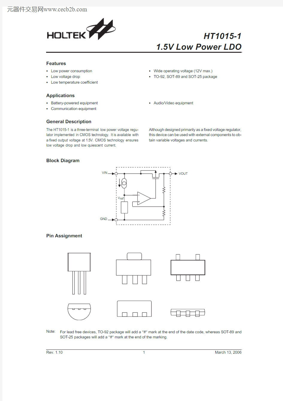
Block Diagram
Pin Assignment
Note:
For lead free devices,TO-92package will add a 2#2mark at the end of the date code,whereas SOT-89and SOT-25packages will add a 2#2mark at the end of the marking.
Rev.1.101March 13,2006
Applications
·Battery-powered equipment ·Communication equipment
·Audio/Video equipment
General Description
The HT1015-1is a three-terminal low power voltage regu-lator implemented in CMOS technology.It is available with a fixed output voltage at 1.5V.CMOS technology ensures low voltage drop and low quiescent current.
Although designed primarily as a fixed voltage regulator,this device can be used with external components to ob-tain variable voltages and currents.
Features
·Low power consumption ·Low voltage drop
·Low temperature coefficient
·Wide operating voltage (12V max.)·TO-92,SOT-89and SOT-25package
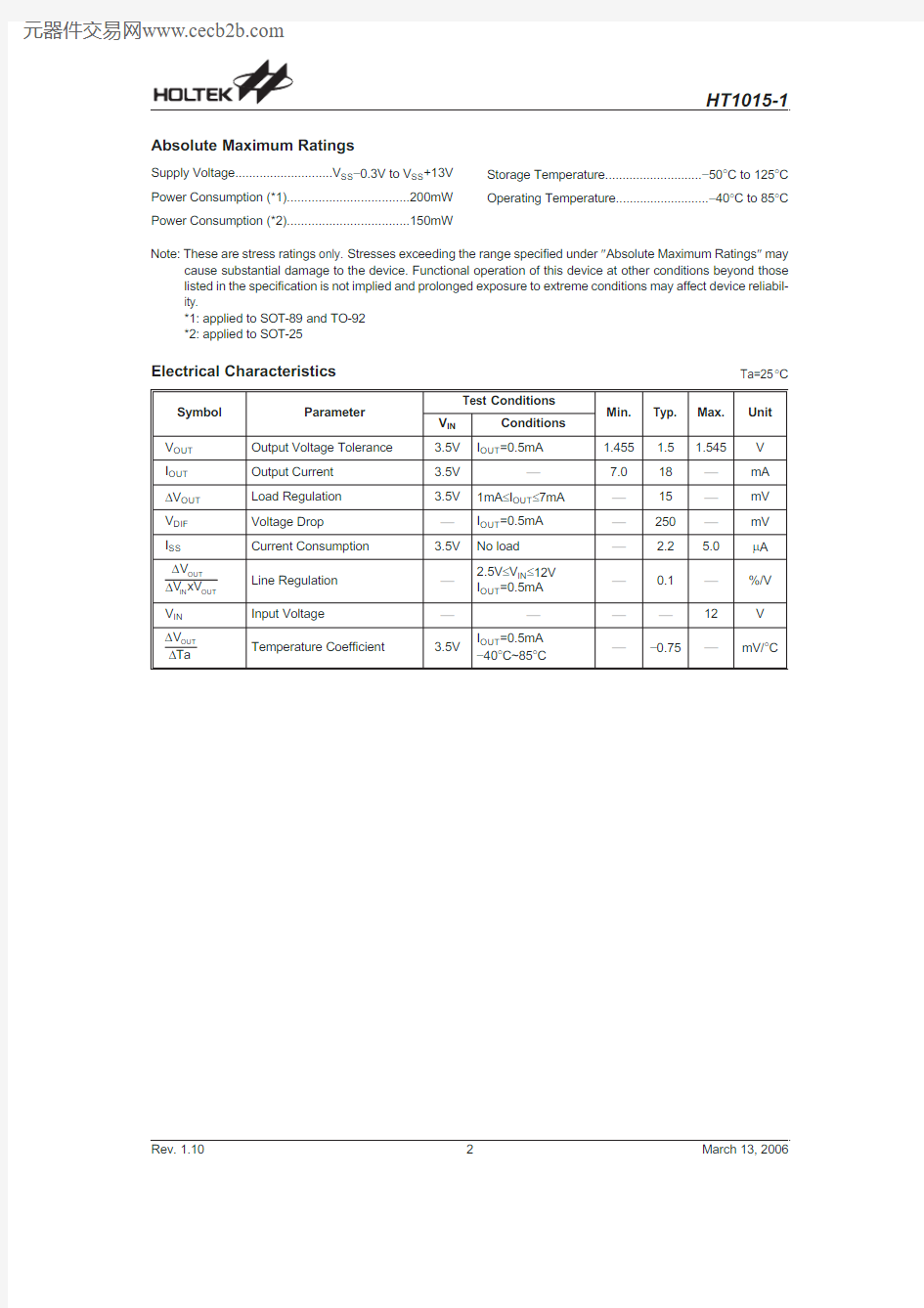
Absolute Maximum Ratings
Supply Voltage............................V SS-0.3V to V SS+13V Storage Temperature............................-50°C to125°C Power Consumption(*1)...................................200mW Operating Temperature...........................-40°C to85°C Power Consumption(*2)...................................150mW
Note:These are stress ratings only.Stresses exceeding the range specified under2Absolute Maximum Ratings2may cause substantial damage to the device.Functional operation of this device at other conditions beyond those listed in the specification is not implied and prolonged exposure to extreme conditions may affect device reliabil-ity.
*1:applied to SOT-89and TO-92
*2:applied to SOT-25
Electrical Characteristics Ta=25°C
Rev.1.102March13,2006
Application Circuits
Basic Circuit
High Output Current Positive Voltage Regulator
Short-Circuit Protection Using External Transistors
Increased Output Voltage Circuits
V=V(1+R2
R1
)+I R2
OUT1XX SS
Rev.1.103March13,2006
V=V+V
OUT1XX D1 Constant Current Regulator
I=V
R
+I
OUT
XX
A
SS
Dual Supply
Rev.1.104March13,2006
Package Information
3-pin TO-92Outline Dimensions
Symbol
Dimensions in mil
Min.Nom.Max.
A170?200
B170?200
C500??
D11?20
E90?110
F45?55
G45?65
H130?160
I8?18
a4°?6°
Rev.1.105March13,2006
Symbol
Dimensions in mm
Min.Nom.Max.
A1? 1.3
A1??0.1
A20.7?0.9
b0.35?0.5
C0.1?0.25
D 2.7? 3.1
E 1.4? 1.8
e? 1.9?
H 2.6?3
L0.37??
q1°?9°
Rev.1.106March13,2006
Symbol
Dimensions in mil
Min.Nom.Max.
A173?181
B64?72
C90?102
D35?47
E155?167
F14?19
G17?22
H?59?
I55?63
J14?17
Rev.1.107March13,2006
Product Tape and Reel Specifications
TO-92Reel Dimensions(Unit:mm)
Rev.1.108March13,2006
Reel Dimensions
SOT-89
Symbol Description Dimensions in mm
A Reel Outer Diameter180±1.0
B Reel Inner Diameter62±1.5
C Spindle Hole Diameter12.75+0.15
D Key Slit Width 1.9±0.15
T1Space Between Flange12.4+0.2
T2Reel Thickness17-0.4
SOT-25
Symbol Description Dimensions in mm
A Reel Outer Diameter178±1
B Reel Inner Diameter62±1
C Spindle Hole Diameter13±0.2
D Key Slit Width 2.5±0.25
T1Space Between Flange8.4+1.5
T2Reel Thickness11.4+1.5
Rev.1.109March13,2006
Carrier Tape Dimensions
TO-92
Symbol Description Dimensions in mm I1Taped Lead Length(2.5)
P Component Pitch12.7±1.0
P0Perforation Pitch12.7±0.3
P2Component to Perforation(Length Direction) 6.35±0.4
F1Lead Spread 2.5+0.4
-0.1
F2Lead Spread 2.5+0.4
-0.1
D h Component Alignment0±0.1
W Carrier Tape Width 18.0+1.0
-0.5
W0Hold-down Tape Width 6.0±0.5
W1Perforation Position9.0±0.5
W2Hold-down Tape Position(0.5)
H0Lead Clinch Height16.0±0.5
H1Component Height Less than24.7
D0Perforation Diameter 4.0±0.2
t Taped Lead Thickness0.7±0.2
H Component Base Height19.0±0.5
Note:Thickness less than0.38±0.05mm~0.5mm
P0Accumulated pitch tolerance:±1mm/20pitches.
()Bracketed figures are for consultation only
Rev.1.1010March13,2006
SOT-89
Symbol Description Dimensions in mm
W Carrier Tape Width 12.0+0.3
-0.1
P Cavity Pitch8.0±0.1
E Perforation Position 1.75±0.1
F Cavity to Perforation(Width Direction) 5.5±0.05
D Perforation Diameter 1.5+0.1
D1Cavity Hole Diameter 1.5+0.1
P0Perforation Pitch 4.0±0.1
P1Cavity to Perforation(Length Direction) 2.0±0.10
A0Cavity Length 4.8±0.1
B0Cavity Width 4.5±0.1
K0Cavity Depth 1.8±0.1
t Carrier Tape Thickness0.30±0.013
C Cover Tape Width9.3
SOT-25
Symbol Description Dimensions in mm W Carrier Tape Width8±0.3
P Cavity Pitch4
E Perforation Position 1.75
F Cavity to Perforation(Width Direction) 3.5±0.05
D Perforation Diameter 1.5+0.1
D1Cavity Hole Diameter 1.5+0.1
P0Perforation Pitch4
P1Cavity to Perforation(Length Direction)2
A0Cavity Length 3.15
B0Cavity Width 3.2
K0Cavity Depth 1.4
t Carrier Tape Thickness0.2±0.03
C Cover Tape Width 5.3
Rev.1.1011March13,2006
Holtek Semiconductor Inc.(Headquarters)
No.3,Creation Rd.II,Science Park,Hsinchu,Taiwan
Tel:886-3-563-1999
Fax:886-3-563-1189
https://www.doczj.com/doc/9715853441.html,
Holtek Semiconductor Inc.(Taipei Sales Office)
4F-2,No.3-2,YuanQu St.,Nankang Software Park,Taipei115,Taiwan
Tel:886-2-2655-7070
Fax:886-2-2655-7373
Fax:886-2-2655-7383(International sales hotline)
Holtek Semiconductor Inc.(Shanghai Sales Office)
7th Floor,Building2,No.889,Yi Shan Rd.,Shanghai,China200233
Tel:021-6485-5560
Fax:021-6485-0313
https://www.doczj.com/doc/9715853441.html,
Holtek Semiconductor Inc.(Shenzhen Sales Office)
43F,SEG Plaza,Shen Nan Zhong Road,Shenzhen,China518031
Tel:0755-8346-5589
Fax:0755-8346-5590
ISDN:0755-8346-5591
Holtek Semiconductor Inc.(Beijing Sales Office)
Suite1721,Jinyu Tower,A129West Xuan Wu Men Street,Xicheng District,Beijing,China100031
Tel:010-6641-0030,6641-7751,6641-7752
Fax:010-6641-0125
Holmate Semiconductor,Inc.(North America Sales Office)
46712Fremont Blvd.,Fremont,CA94538
Tel:510-252-9880
Fax:510-252-9885
https://www.doczj.com/doc/9715853441.html,
Copyrightó2006by HOLTEK SEMICONDUCTOR INC.
The information appearing in this Data Sheet is believed to be accurate at the time of publication.However,Holtek as-sumes no responsibility arising from the use of the specifications described.The applications mentioned herein are used solely for the purpose of illustration and Holtek makes no warranty or representation that such applications will be suitable without further modification,nor recommends the use of its products for application that may present a risk to human life due to malfunction or otherwise.Holtek¢s products are not authorized for use as critical components in life support devices or systems.Holtek reserves the right to alter its products without prior notification.For the most up-to-date information, please visit our web site at https://www.doczj.com/doc/9715853441.html,.
Rev.1.1012March13,2006