DVFL2800S Series
HIGH RELIABILITY HYBRID
DC-DC CONVERTERS
DESCRIPTION
The DVFL series of high reliability DC-DC converters
is operable over the full military (-55 °C to +125 °C) temperature range with no power derating. Unique to the DVFL series is a magnetic feedback circuit that is radiation immune. Operating at a nominal fixed frequency of 500 kHz, these regulated, isolated units utilize well-controlled undervoltage lockout circuitry to eliminate slow start-up problems. The current sharing function allows a maximum of five units to be connected in parallel to boost the total
output power to 5 times. The output voltage is
trimmable up to +10% or down –20%.
These converters are designed and manufactured in
a facility qualified to ISO9001 and certified to MIL-PRF-38534 and MIL-STD-883.
This product may incorporate one or more of the
following U.S. patents:
5,784,266
5,790,389
5,963,438 5,999,433 6,005,780 6,084,792 6,118,673 FEATURES
? High Reliability ? Parallel Up to 5 Units With Current Sharing ? Output Voltage Trim Up +10% or Down –20% ? Wide Input Voltage Range: 16 to 40 Volts per MIL-STD-704 ? Up to 120 Watts Output Power ? Radiation Immune Magnetic Feedback Circuit ? NO Use of Optoisolators ? Undervoltage Lockout ? Indefinite Short Circuit Protection
? Current Limit Protection
? Industry Standard Pinout
? Input Transient Voltage: 50 Volts for 1 second ? Radiation Hardened Version Available ? Precision Seam Welded Hermetic Package ? High Power Density: > 80 W/in 3 ? Custom Versions Available ? Additional Environmental Screening Available ? Meets MIL-STD-461C and MIL-STD-461D EMC Requirements When Used With a DVME28 EMI Filter
? MIL-PRF-38534 Element Evaluated Components
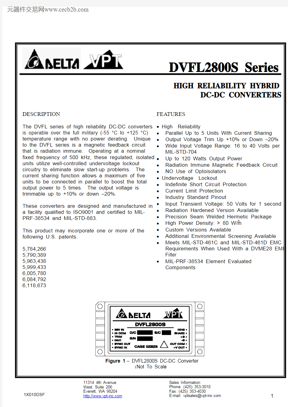
Figure 1 – DVFL2800S DC-DC Converter
(Not To Scale )
DVFL2800S Series
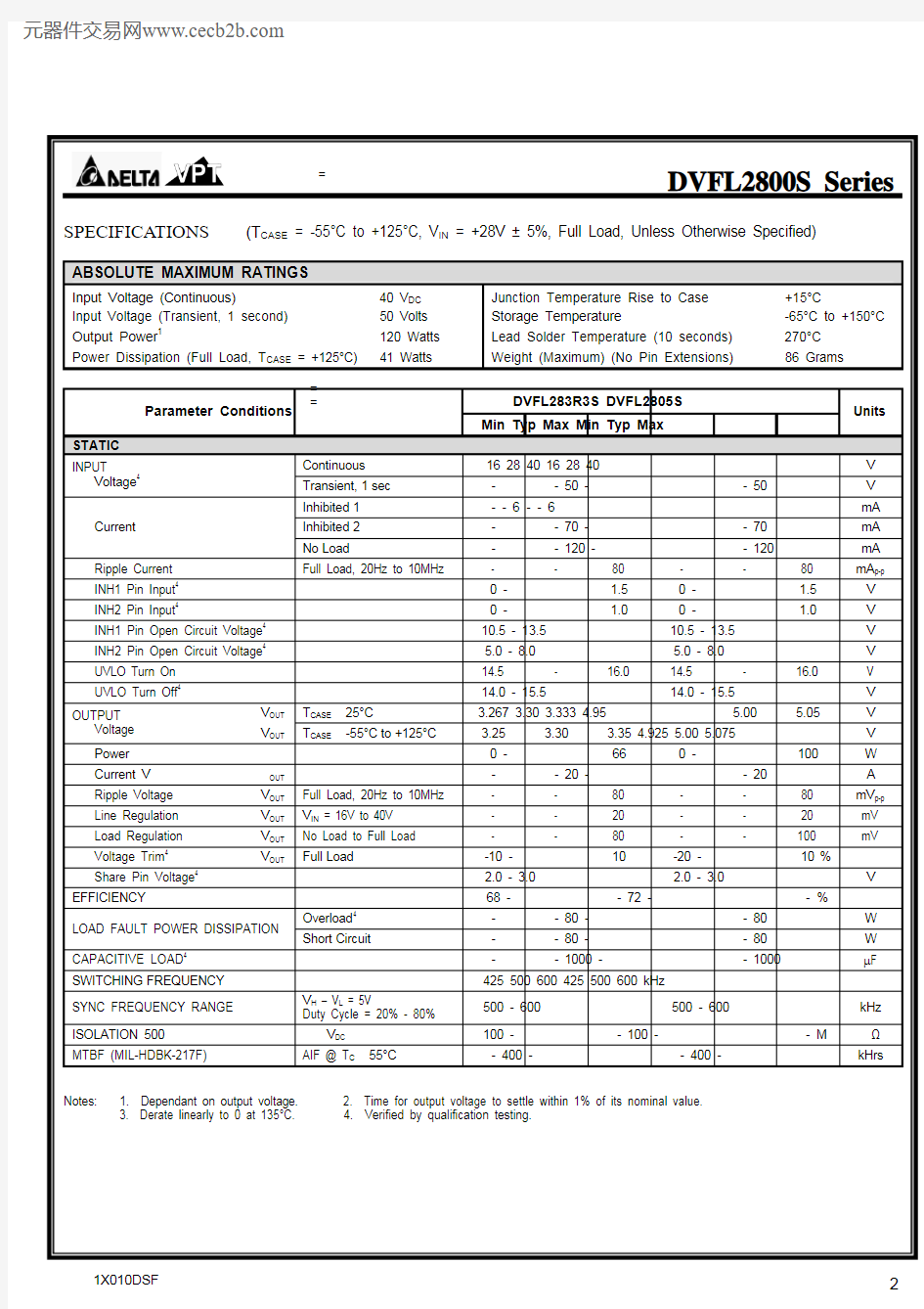
SPECIFICATIONS (T CASE = -55°C to +125°C, V IN = +28V ± 5%, Full Load, Unless Otherwise Specified)
ABSOLUTE MAXIMUM RATINGS
Input Voltage (Continuous)
40 V DC Junction Temperature Rise to Case +15°C
Input Voltage (Transient, 1 second) 50 Volts Storage Temperature
-65°C to +150°C Output Power 1
120 Watts Lead Solder Temperature (10 seconds) 270°C Power Dissipation (Full Load, T CASE = +125°C)
41 Watts
Weight (Maximum) (No Pin Extensions)
86 Grams
DVFL283R3S DVFL2805S
Parameter Conditions Min Typ Max Min Typ Max
Units
STATIC
Continuous 16 28 40 16 28 40 V INPUT
Voltage
4
Transient, 1 sec - - 50 - - 50 V
Inhibited 1 - - 6 - - 6 mA Inhibited 2 - - 70 - - 70 mA
Current
No Load - - 120 - - 120 mA Ripple Current Full Load, 20Hz to 10MHz -
-
80
-
-
80
mA p-p
INH1 Pin Input 4 0 - 1.5 0 - 1.5 V INH2 Pin Input
4
0 - 1.0 0 - 1.0 V
INH1 Pin Open Circuit Voltage 4 10.5 - 13.5 10.5 - 13.5 V INH2 Pin Open Circuit Voltage 4
5.0 - 8.0 5.0 - 8.0 V UVLO Turn On 14.5
-
16.0
14.5
-
16.0
V
UVLO Turn Off 4
14.0 - 15.5 14.0 - 15.5 V V OUT T CASE =
25°C 3.267 3.30 3.333 4.95 5.00 5.05 V
OUTPUT
Voltage
V OUT
T CASE = -55°C to +125°C 3.25 3.30 3.35 4.925 5.00 5.075 V
Power
0 - 66 0 - 100 W
Current V OUT
- - 20 - - 20 A Ripple Voltage V OUT Full Load, 20Hz to 10MHz - - 80 - - 80 mV p-p Line Regulation V OUT V IN = 16V to 40V - - 20 - - 20 mV Load Regulation V OUT No Load to Full Load -
-
80
-
-
100
mV
Voltage Trim
4
V OUT
Full Load -10 - 10 -20 - 10 % Share Pin Voltage
4
2.0 -
3.0 2.0 - 3.0 V EFFICIENCY
68 - - 72 - - % Overload 4
- - 80 - - 80 W LOAD FAULT POWER DISSIPATION Short Circuit
- - 80 - - 80 W CAPACITIVE LOAD
4
- - 1000 - - 1000 μF SWITCHING FREQUENCY
425 500 600 425 500 600 kHz
SYNC FREQUENCY RANGE
V H – V L = 5V
Duty Cycle = 20% - 80% 500 - 600 500 - 600 kHz
ISOLATION 500 V DC 100 - - 100 - - M ? MTBF (MIL-HDBK-217F)
AIF @ T C =
55°C
- 400 - - 400 - kHrs
Notes:
1. Dependant on output voltage.
2. Time for output voltage to settle within 1% of its nominal value.
3. Derate linearly to 0 at 135°C.
4. Verified by qualification testing.
DVFL2800S Series
SPECIFICATIONS (T CASE = -55°C to +125°C, V IN = +28V ± 5%, Full Load, Unless Otherwise Specified)
ABSOLUTE MAXIMUM RATINGS
Input Voltage (Continuous)
40 V DC Junction Temperature Rise to Case +15°C
Input Voltage (Transient, 1 second) 50 Volts Storage Temperature
-65°C to +150°C Output Power 1
120 Watts Lead Solder Temperature (10 seconds) 270°C Power Dissipation (Full Load, T CASE = +125°C)
41 Watts
Weight (Maximum) (No Pin Extensions)
86 Grams
DVFL283R3S DVFL2805S
Parameter Conditions Min Typ Max Min Typ Max
Units
DYNAMIC
Load Step Output Transient V OUT - - 400 - - 400 mV PK Load Step Recovery 2
Half Load to Full Load - - 500 - - 500 μSec Line Step Output Transient 4
V OUT - 300 600 - 300 600 mV PK Line Step Recovery 2, 4
V IN = 16V to 40V - 300 500 - 300 500 μSec Turn On Delay
V OUT
- - 20 - - 20 mSec
Turn On Overshoot
V IN = 0V to 28V
- - 15 - - 25 mV PK
Notes:
1. Dependant on output voltage.
2. Time for output voltage to settle within 1% of its nominal value.
3. Derate linearly to 0 at 135°C.
4. Verified by qualification testing.
DVFL2800S Series
SPECIFICATIONS (T CASE = -55°C to +125°C, V IN = +28V ± 5%, Full Load, Unless Otherwise Specified)
ABSOLUTE MAXIMUM RATINGS
Input Voltage (Continuous)
40 V DC Junction Temperature Rise to Case +15°C
Input Voltage (Transient, 1 second) 50 Volts Storage Temperature
-65°C to +150°C Output Power 1
120 Watts Lead Solder Temperature (10 seconds) 270°C Power Dissipation (Full Load, T CASE = +125°C)
41 Watts
Weight (Maximum) (No Pin Extensions)
86 Grams
DVFL2812S DVFL2815S
Parameter Conditions Min Typ Max Min Typ Max
Units
STATIC
Continuous 16 28 40 16 28 40 V INPUT
Voltage
4
Transient, 1 sec - - 50 - - 50 V
Inhibited 1 - - 6 - - 6 mA Inhibited 2 - - 70 - - 70 mA
Current
No Load - - 120 - - 120 mA Ripple Current Full Load, 20Hz to 10MHz -
-
80
-
-
80
mA p-p
INH1 Pin Input 4 0 - 1.5 0 - 1.5 V INH2 Pin Input
4
0 - 1.0 0 - 1.0 V
INH1 Pin Open Circuit Voltage 4 10.5 - 13.5 10.5 - 13.5 V INH2 Pin Open Circuit Voltage 4
5.0 - 8.0 5.0 - 8.0 V UVLO Turn On 14.5
-
16.0
14.5
-
16.0
V
UVLO Turn Off 4
14.0 - 15.5 14.0 - 15.5 V V OUT T CASE =
25°C
11.88 12.00 12.12 14.85 15.00 15.15 V OUTPUT
Voltage
V OUT
T CASE = -55°C to +125°C 11.82 12.00 12.18 14.775 15.00 15.225 V Power
- - 110 - - 120 W Current V OUT
- - 9.2 - - 8.0 A
Ripple Voltage V OUT Full Load, 20Hz to 10MHz - - 80 - - 80 mV p-p Line Regulation V OUT V IN = 16V to 40V - - 20 - - 20 mV Load Regulation V OUT No Load to Full Load -
-
120
-
-
120
mV
Voltage Trim
4
V OUT
Full Load -20 - 10 -20 - 10 % Share Pin Voltage
4
2.0 -
3.0 2.0 - 3.0 V EFFICIENCY
79 - - 80 - - % Overload
4
- - 80 - - 80 W LOAD FAULT POWER DISSIPATION Short Circuit - - 80 - - 80 W CAPACITIVE LOAD
4
- - 500 - - 500 μF SWITCHING FREQUENCY
425 500 600 425 500 600 kHz
SYNC FREQUENCY RANGE
V H – V L = 5V
Duty Cycle = 20% - 80% 500 - 600 500 - 600 kHz
ISOLATION 500 V DC 100 - - 100 - - M ? MTBF (MIL-HDBK-217F)
AIF @ T C =
55°C
- 400 - - 400 - kHrs
Notes:
1. Dependant on output voltage.
2. Time for output voltage to settle within 1% of its nominal value.
3. Derate linearly to 0 at 135°C.
4. Verified by qualification testing.
DVFL2800S Series
SPECIFICATIONS (T CASE = -55°C to +125°C, V IN = +28V ± 5%, Full Load, Unless Otherwise Specified)
ABSOLUTE MAXIMUM RATINGS
Input Voltage (Continuous)
40 V DC Junction Temperature Rise to Case +15°C
Input Voltage (Transient, 1 second) 50 Volts Storage Temperature
-65°C to +150°C Output Power 1
120 Watts Lead Solder Temperature (10 seconds) 270°C Power Dissipation (Full Load, T CASE = +125°C)
41 Watts
Weight (Maximum) (No Pin Extensions)
86 Grams
DVFL2812S DVFL2815S
Parameter Conditions Min Typ Max Min Typ Max
Units
DYNAMIC
Load Step Output Transient V OUT - - 800 - - 800 mV PK Load Step Recovery 2
Half Load to Full Load - - 500 - - 500 μSec Line Step Output Transient 4
V OUT - 600 1200 - 600 1200 mV PK Line Step Recovery 2, 4
V IN = 16V to 40V - 300 500 - 300 500 μSec Turn On Delay
V OUT
- - 20 - - 20 mSec
Turn On Overshoot
V IN = 0V to 28V
- - 50 - - 50 mV PK
Notes:
1. Dependant on output voltage.
2. Time for output voltage to settle within 1% of its nominal value.
3. Derate linearly to 0 at 135°C.
4. Verified by qualification testing.
DVFL2800S Series SPECIFICATIONS (T CASE = -55°C to +125°C, V IN = +28V ± 5%, Full Load, Unless Otherwise Specified)
ABSOLUTE MAXIMUM RATINGS
Input Voltage (Continuous) 40 V DC Junction Temperature Rise to Case +15°C
Input Voltage (Transient, 1 second) 50 Volts Storage Temperature -65°C to +150°C Output Power1120 Watts Lead Solder Temperature (10 seconds) 270°C
Power Dissipation (Full Load, T CASE = +125°C) 41 Watts Weight (Maximum) (No Pin Extensions) 86 Grams
DVFL285R2S
Parameter Conditions
Min Typ Max
Units
STATIC
Continuous 16 28 40 V
INPUT
Voltage4 Transient, 1 sec - - 50 V
Inhibited 1 - - 6 mA
Inhibited 2 - - 70 mA
Current
No Load - - 120 mA
Ripple Current Full Load, 20Hz to 10MHz - - 80 mA p-p
INH1 Pin Input4 0
-
1.5
V INH2 Pin Input4 0
-
1.0
V INH1 Pin Open Circuit Voltage4 10.5
-
13.5
V INH2 Pin Open Circuit Voltage4 5.0
-
8.0
V UVLO Turn On 14.5 - 16.0 V
UVLO Turn Off4 14.0
-
15.5
V
V OUT T CASE = 25°C 5.148 5.20 5.252 V
OUTPUT
Voltage V
OUT
T CASE = -55°C to +125°C 5.122 5.20 5.278 V
Power -
-
100
W Current V OUT -
-
19.2
A Ripple Voltage V OUT Full Load, 20Hz to 10MHz - - 80 mV p-p
Line Regulation V OUT V IN = 16V to 40V - - 20 mV
Load Regulation V OUT No Load to Full Load - - 100 mV
Voltage Trim4 V OUT Full Load -20 - 10 %
Share Pin Voltage4 2.0
-
3.0
V EFFICIENCY 72
-
-
%
Overload4 - - 80 W
LOAD FAULT POWER DISSIPATION
Short Circuit - - 80 W
CAPACITIVE LOAD4 -
-
1000
μF
SWITCHING
FREQUENCY 425 500 600 kHz
SYNC FREQUENCY RANGE V H – V L = 5V
Duty Cycle = 20% - 80%
500 - 600 kHz
ISOLATION 500
V DC 100 - - M?MTBF (MIL-HDBK-217F) AIF @ T C = 55°C - 400 - kHrs
Notes: 1. Dependant on output voltage. 2. Time for output voltage to settle within 1% of its nominal value.
3. Derate linearly to 0 at 135°C.
4. Verified by qualification testing.
DVFL2800S Series
SPECIFICATIONS (T CASE = -55°C to +125°C, V IN = +28V ± 5%, Full Load, Unless Otherwise Specified)
ABSOLUTE MAXIMUM RATINGS
Input Voltage (Continuous)
40 V DC Junction Temperature Rise to Case +15°C
Input Voltage (Transient, 1 second) 50 Volts Storage Temperature
-65°C to +150°C Output Power 1
120 Watts Lead Solder Temperature (10 seconds) 270°C Power Dissipation (Full Load, T CASE = +125°C)
41 Watts
Weight (Maximum) (No Pin Extensions)
86 Grams
DVFL285R2S
Parameter Conditions Min Typ Max
Units
DYNAMIC
Load Step Output Transient V OUT - - 400 mV PK Load Step Recovery 2
Half Load to Full Load - - 500 μSec Line Step Output Transient 4
V OUT - 300 600 mV PK Line Step Recovery 2, 4
V IN = 16V to 40V - 300 500 μSec
Turn On Delay
V OUT
- - 20 mSec Turn On Overshoot
V IN = 0V to 28V
- - 25 mV PK
Notes: 1. Dependant on output voltage. 2. Time for output voltage to settle within 1% of its nominal value. 3. Derate linearly to 0 at 135°C. 4. Verified by qualification testing.
DVFL2800S Series
BLOCK DIAGRAM
UND ER VOLTAGE SHU TDOWN
PRIMAR Y HOUSEKEEPIN G
SUPPLY
PWM CONTR OL
VOLTAGE AND CUR RENT AMPLIFIER S
SEC ON DARY HOUSEKEEPIN G
SUPPLY
PIN 1
28V IN
PIN 2
IN C OM
Q1
+V OUT PIN 7
PIN 8
OUT COM
INH1
PIN 4
FEEDBACK
MAGNETIC SYN C IN
PIN 6
SYN C OUT
PIN 5
TRIM
PIN 3
+S
PIN 10
-S
PIN 9
SHARE
PIN 11
INH2
PIN 12
Figure 2
CONNECTION DIAGRAM
2
IN COM 4
INH1
1
28V IN
7
+V OUT
8OUT COM
LOAD
+-
28 Vdc
-S
9
+S
10
INH2
12
SYNC IN
6
Figure 3
DVFL2800S Series
INHIBIT DRIVE CONNECTION DIAGRAM
2
IN COM 4
INH11
28V IN OPTIONAL CAPACITOR BIAS 1
12V
30K
OPTOISOLATOR
+-8V
2K BIAS 2
INH2
12OUT COM
8
Figure 4 – Isolated Inhibit Drive and Internal Equivalent Circuit
(Shown with optional capacitor for turn-on delay)
EMI FILTER HOOKUP DIAGRAM
2
IN COM 4
INH1
1
28V IN
7
+V OUT
8
OUT COM
LOAD
+-
28 Vdc
12
28V OUT
7
OUT COM
1
28V IN
6
IN COM
CASE
-S
9
+S
10
INH2
12
SYNC IN
6
28V IN
2
28V IN
3
IN COM
4
IN COM
5
28V OUT
11
28V OUT
10
OUT COM
9
OUT COM
8
DVME28 EMI FILTER
DVFL2800S DC-DC CONVERTER
Figure 5 – Converter with EMI Filter
DVFL2800S Series
PARALLEL CONNECTION DIAGRAMS
2
IN COM 4
INH1
1
28V IN
7
+V OUT
8
OUT COM
LOAD
+-
28 Vdc
12
28V OUT
7
OUT COM 1
28V IN
6
IN COM
CASE
-S
9
+S
10
SYNC IN
6
28V IN
2
28V IN
3
IN COM
4
IN COM
5
28V OUT
11
28V OUT
10
OUT COM
9
OUT COM
8
DVME28 EMI FILTER
DVFL2800S DC-DC CONVERTER
CASE
2
IN COM 4
INH1
1
28V IN
7
+V OUT
8
OUT COM
-S
9
+S
10
SYNC IN
6
DVFL2800S DC-DC CONVERTER
CASE
Figure 6 – Parallel Connection without Current Sharing
DVFL2800S Series
PARALLEL CONNECTION DIAGRAMS
2
IN COM 4
INH1
1
28V IN
7
+V OUT
8
OUT COM
LOAD
+-
28 Vdc
12
28V OUT
7
OUT COM 1
28V IN
6
IN COM
CASE
-S
9
+S
10
SYNC IN
6
28V IN
2
28V IN
3
IN COM
4
IN COM
5
28V OUT
11
28V OUT
10
OUT COM
9
OUT COM
8
DVME28 EMI FILTER
DVFL2800S DC-DC CONVERTER
CASE
5
SYNC OUT
11
SHARE
2
IN COM 4
INH1
1
28V IN
7
+V OUT
8OUT COM
-S
9
+S
10
SYNC IN
6
DVFL2800S DC-DC CONVERTER
CASE
5
SYNC OUT
11
SHARE
2
IN COM 4
INH1
1
28V IN
7
+V OUT
8
OUT COM
-S
9
+S
10
SYNC IN
6
DVFL2800S DC-DC CONVERTER CASE
11
SHARE
Figure 7 – Current Sharing Parallel Connection for Multiple Converters
DVFL2800S Series OUTPUT VOLTAGE TRIM
The output voltage can be trimmed down by
connecting a resistor between the TRIM pin
(PIN 3) and the +V OUT pin (PIN 7), or can
be trimmed up by connecting a resistor
between the TRIM pin (PIN 3) and the OUT
COM pin (PIN 8). The maximum trim range
is +10% up and –20% down. The
appropriate resistor values versus the
output voltage are given in the trim table
below.
Figure 8 – Output Voltage Trim
DVFL283R3S DVFL2805S DVFL285R2S DVFL2812S DVFL2815S
+V OUT (V) R TRIM (?) +V OUT (V) R TRIM (?) +V OUT (V) R TRIM (?) +V OUT (V) R TRIM (?) +V OUT (V) R TRIM (?)
3.60 68.3k 5.5 35k 5.7 35k 13.2 5.8k 16.50 1.7k
3.55 85k 5.4 47.5k 5.6 47.5k 13.0 10k 16.25 5k
3.50 110k 5.3 68.3k 5.5 68.3k 12.8 16.2k 16.00 10k
3.45 151.7k 5.2 110k 5.4 110k 12.6 26.6k 15.75 18.3k
3.40 235k 5.1 235k 5.3 235k 12.4 47.3k 15.50 35k
3.35 485k 5.0 - 5.2 - 12.2 109k
15.25
85k
3.30 -
4.9 225k
5.1 245k 12.0 - 15.00 -
3.25 135k
4.8 100k
5.0 110k 11.8 454k 14.75 475k
3.20 55k
4.7 58.3k 4.9 65k 11.6 213k 14.50 225k
3.15 28.3k
4.6 37.5k 4.8 42.5k 11.4 134k 14.25 142k
3.10 15k
4.5 25k 4.7 29k 11.2 94k 14.00 100k
3.05 7k
4.4 16.7k 4.6 20k 11.0 70.1k 13.75 75k
3.00 1.7k
4.3 10.7k 4.5 13.6k 10.8 54.3k 13.50 58.3k
4.2
6.3k
4.4
8.8k 10.6 42.9k 13.25 46.4k
4.1
2.8k
4.3
5k
10.4 34.4k 13.00 37.5k
4.0 0 4.2
2k
10.2 27.8k 12.75 30.6k
10.0
22.5k
12.50
25k
9.8
18.2k
12.25
20.5k
9.6
14.6k
12.00
16.7k
DVFL2800S Series
EFFICIENCY PERFORMANCE CURVES (T CASE = 25°C, Full Load, Unless Otherwise Specified)
V IN = 16V V IN = 28V V IN = 40V
6570
75
80
85
10
20
30
40
50
60
70
Output P ow er (W)
E f f i c i e n c y (%)
70
75
8085
204060
80100
Output P ow er (W)
E f f i c i e n c y (%)
Figure 9 – DVFL283R3S Figure 10 – DVFL2805S / DVFL285R2S Efficiency (%) vs. Output Power (W)
Efficiency (%) vs. Output Power (W)
7075
80
85
90
30
50
70
90
110
Output P ow er (W)
E f f i c i e n c y (%)
7075
80
85
90
30
50
70
90
110
Output Pow er (W)
E f f i c i e n c y (%)
Figure 11 – DVFL2812S Figure 12 – DVFL2815S Efficiency (%) vs. Output Power (W)
Efficiency (%) vs. Output Power (W)
DVFL2800S Series EMI PERFORMANCE CURVES
(T CASE = 25°C, V IN = +28V ± 5%, Full Load, Unless Otherwise Specified)
Figure 13 – DVFL2800S without EMI Filter
Figure 14 – DVFL2800S with EMI Filter
DVFL2800S Series PACKAGE SPECIFICATIONS
TOP VIEW
PIN FUNCTION
IN
1 28V
COM
2 IN
3 TRIM
4 INH1
OUT
5 SYNC
6 SYNC
IN
OUT
7 +V
COM
8 OUT
9 -S
10 +S
11 SHARE
12 INH2
SIDE VIEW
Figure 15 – Package and Pinout
(Pin Length is ±0.01”, Other Dimensional Limits are ±0.005” Unless Otherwise Stated)
DVFL2800S Series PACKAGE SPECIFICATIONS (DOWN-LEADED)
TOP VIEW
PIN FUNCTION
IN
1 28V
COM
2 IN
3 TRIM
4 INH1
OUT
5 SYNC
6 SYNC
IN
OUT
7 +V
COM
8 OUT
9 -S
10 +S
11 SHARE
12 INH2
SIDE VIEW
Figure 16 – Package and Pinout (With Down-Leaded Pin Extensions Added)
DVFL2800S Series PACKAGE SPECIFICATIONS (UP-LEADED)
TOP VIEW
PIN FUNCTION
IN
1 28V
COM
2 IN
3 TRIM
4 INH1
OUT
5 SYNC
6 SYNC
IN
OUT
7 +V
COM
8 OUT
9 -S
10 +S
11 SHARE
12 INH2
SIDE VIEW
Figure 17 – Package and Pinout (With Up-Leaded Pin Extensions Added)
DVFL2800S Series PACKAGE PIN DESCRIPTION
Pin Function Description
1 28V IN Positive Input Voltage Connection
2 IN COM Input Common Connection
3 TRIM Trim Output Voltage to +10%, -20% of Nominal Value
4 INH1Logic Low = Disabled Output. Connecting the inhibit(1) pin to input common causes converter shutdown.
Logic High = Enabled Output. Unconnected or open collector TTL.
5 SYNC OUT Output Synchronization Signal
6 SYNC IN Input Synchronization Signal
7 +V OUT Positive Output Voltage Connection
8 OUT COM Output Common Connection
9 -S Return
Sense
10 +S Positive
Sense
11 SHARE Current
Share
12 INH2 Logic Low = Disabled Output. Connecting the inhibit(2) pin to output common causes converter shutdown.
Logic High = Enabled Output. Unconnected or open collector TTL.
DVFL2800S Series
ENVIRONMENTAL SCREENING (100% Tested Per MIL-STD-883 as referenced to MIL-PRF-38534)
Notes:
1. 100% R&R testing at –55°C, +25°C, and +125°C with all test data included in product shipment.
2. PIND test Certificate of Compliance included in product shipment.
3. Radiographic test Certificate of Compliance and film(s) included in product shipment.
Screening MIL-STD-883
Standard
(No Suffix)
Extended /ES HB /HB
Class H
/H
Class K /K
Non-Destructive Bond Pull Method 2023 ? ? ? ? ? Internal Visual Method 2017, 2032 Internal Procedure
? ? ? ? ? Temperature Cycling Method 1010, Condition C Method 1010, -55°C to 125°C ? ? ? ? Constant Acceleration Method 2001, 3000g, Y1 Direction Method 2001, 500g, Y1 Direction ? ? ? ? PIND Method 2020, Condition A 2
?
Pre Burn-In Electrical
100% at 25°C ? Burn-In
Method 1015, 320 hours at +125°C Method 1015, 160 hours at +125°C 96 hours at +125°C 24 hours at +125°C ? ? ? ? ? Final Electrical
MIL-PRF-38534, Group A 1 100% at 25°C
? ? ? ? ? Hermeticity
Method 1014, Fine Leak, Condition A Method 1014, Gross Leak, Condition C
Dip (1 x 10⁻³
)
? ? ? ? ? ? ? ? ? Radiography Method 20123 ? External Visual
Method 2009
?
?
?
?
?
DVFL2800S Series ORDERING INFORMATION
DVFL 28 05 S R DL /HB - XXX
1 2 3 4 5 6 7 8
(1) (2) (3) (4)
Product Series Nominal Input
Voltage
Output Voltage Number of Outputs
DVFL 28 28 Volts 3R3
05
5R2
12
15 3.3 Volts
5 Volts
5.2 Volts
12 Volts
15 Volts
S Single
(5) (6) (7) (8)
Rad-Hard Option2 Package Option Screening Code1,3 Additional Screening
Code
None R Standard
100 kRad
None
DL
UL
Standard
Down-Lead
Up-Lead
None
/ES
/HB
/H
/K
Standard
Extended
HB
Class H
Class K
Contact Sales
Notes: 1. Contact the VPT Inc. Sales Department for availability of Class H (/H) or Class K (/K) qualified products.
2. VPT Inc. is not currently qualified to a DSCC certified radiation hardness assurance program.
3. VPT Inc. reserves the right to ship higher screened or SMD products to meet lower screened orders at our
sole discretion unless specifically forbidden by customer contract.
Please contact your sales representative or the VPT Inc. Sales Department for more information concerning additional environmental screening and testing, different input voltage, output voltage, power requirement, source inspection, and/or special element evaluation for space or other higher quality applications.