LMK04100,LMK04101,LMK04102,LMK04110, LMK04111,LMK04131,LMK04133
LMK04100 Family Clock Jitter Cleaner with Cascaded PLLs
Literature Number: SNAS516A
LMK04100 Family INFORMATION
September 19, 2011 Clock Jitter Cleaner with Cascaded PLLs
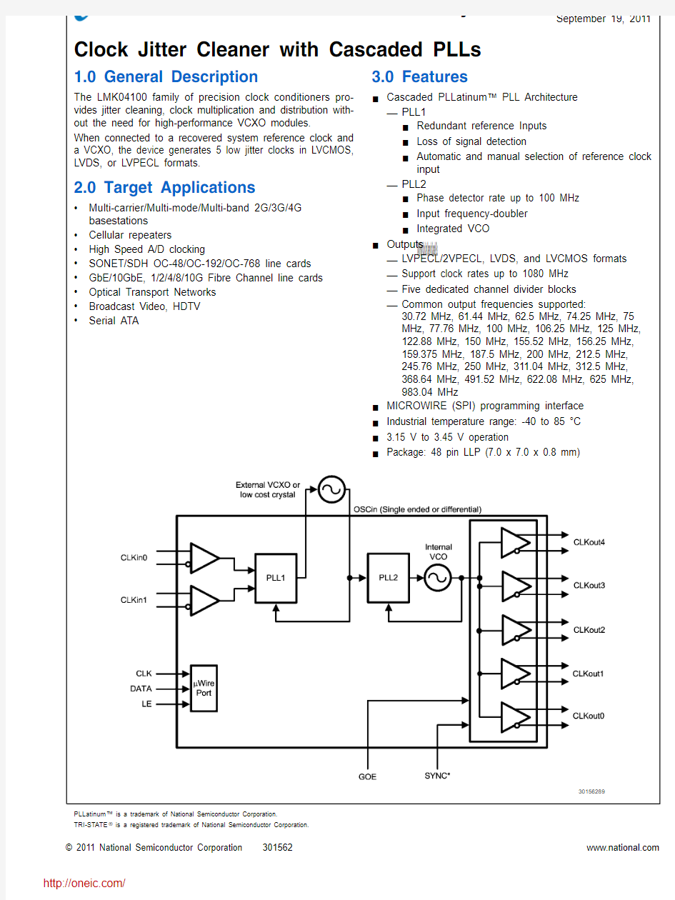
1.0 General Description
The LMK04100 family of precision clock conditioners pro-vides jitter cleaning, clock multiplication and distribution with-out the need for high-performance VCXO modules.
When connected to a recovered system reference clock and a VCXO, the device generates 5 low jitter clocks in LVCMOS, LVDS, or LVPECL formats.
2.0 Target Applications
?Multi-carrier/Multi-mode/Multi-band 2G/3G/4G basestations
?Cellular repeaters
?High Speed A/D clocking
?SONET/SDH OC-48/OC-192/OC-768 line cards
?GbE/10GbE, 1/2/4/8/10G Fibre Channel line cards ?Optical Transport Networks
?Broadcast Video, HDTV
?Serial ATA 3.0 Features
■Cascaded PLLatinum? PLL Architecture
—PLL1
■Redundant reference Inputs
■Loss of signal detection
■Automatic and manual selection of reference clock input
—PLL2
■Phase detector rate up to 100 MHz
■Input frequency-doubler
■Integrated VCO
■Outputs
—LVPECL/2VPECL, LVDS, and LVCMOS formats
—Support clock rates up to 1080 MHz
—Five dedicated channel divider blocks
—Common output frequencies supported:
30.72 MHz, 61.44 MHz, 62.5 MHz, 74.25 MHz, 75
MHz, 77.76 MHz, 100 MHz, 106.25 MHz, 125 MHz,
122.88 MHz, 150 MHz, 155.52 MHz, 156.25 MHz,
159.375 MHz, 187.5 MHz, 200 MHz, 212.5 MHz,
245.76 MHz, 250 MHz, 311.04 MHz, 312.5 MHz,
368.64 MHz, 491.52 MHz, 622.08 MHz, 625 MHz,
983.04 MHz
■MICROWIRE (SPI) programming interface
■Industrial temperature range: -40 to 85 °C
■ 3.15 V to 3.45 V operation
■Package: 48 pin LLP (7.0 x 7.0 x 0.8 mm)
30156289
PLLatinum? is a trademark of National Semiconductor Corporation.
TRI-STATE? is a registered trademark of National Semiconductor Corporation.
? 2011 National Semiconductor https://www.doczj.com/doc/bc2148699.html, K04100 Family Clock Jitter Cleaner with Cascaded PLLs
NSID 2VPECL / LVPECL
OUTPUTS
LVDS OUTPUTS
LVCMOS OUTPUTS
VCO
LMK04100SQ 3 41185 to 1296 MHz LMK04101SQ 3 41430 to 1570 MHz LMK04102SQ 3 41600 to 1750 MHz LMK04110SQ 5 1185 to 1296 MHz LMK04111SQ 5 1430 to 1570 MHz LMK04131SQ 2221430 to 1570 MHz LMK04133SQ
2
2
2
1840 to 2160 MHz
TABLE 2. Device Output Format Information
NSID CLKout0CLKout1CLKout2CLKout3
CLKout4
LMK04100SQ 2VPECL / LVPECL LVCMOS x 2LVCMOS x 22VPECL / LVPECL 2VPECL / LVPEC
LMK04101SQ 2VPECL / LVPECL LVCMOS x 2LVCMOS x 22VPECL / LVPECL 2VPECL / LVPEC
LMK04102SQ 2VPECL / LVPECL
LVCMOS x 2
LVCMOS x 2
2VPECL / LVPECL 2VPECL / LVPEC
LMK04110SQ 2VPECL / LVPECL 2VPECL / LVPECL 2VPECL / LVPECL 2VPECL / LVPECL 2VPECL / LVPEC
LMK04111SQ 2VPECL / LVPECL 2VPECL / LVPECL 2VPECL / LVPECL 2VPECL / LVPECL 2VPECL / LVPEC
LMK04131SQ LVDS 2VPECL / LVPECL LVCMOS x 22VPECL / LVPECL LVDS LMK04133SQ
LVDS
2VPECL / LVPECL
LVCMOS x 2
2VPECL / LVPECL
LVDS
TABLE 3. Example Configurations for Common Frequencies
OSCin (MHz)
VCO Divider
PLL2 N VCO Frequency
(Note 1)
Output Divider
Output Frequency
Application
2523015001262.5GigE 2523015001075SATA 24.88322251244.16877.76SONET 2522412006100PCI Express
26.5625781487.52106.25Fibre Channe
2523015006125GigE 2551215002150SATA 24.88322251244.164155.52SONET 2522512504156.2510 GigE 26.562522512754159.37510-G Fibre Channel 2522515004187.512 GigE 2531612002200PCI Express 26.562531612752212.54-G Fibre Channel 2532015002250GigE 24.88322251244.162311.04SONET 2522512502312.5XGMII 24.88322251244.161622.08SONET 25
2
25
1200
1
625
10 GigE
Note 1:Use VCO Frequency to select proper device option
Table 3 shows a limited list of example frequencies. Multiple output frequencies can be programmed on a single device provid that the VCO frequency and VCO divider values are the same.
https://www.doczj.com/doc/bc2148699.html, 2
L M K 04100
30156201
https://www.doczj.com/doc/bc2148699.html, 04100 Family
1.0 General Description .........................................................................................................................2.0 Target Applications ..........................................................................................................................3.0 Features ........................................................................................................................................TABLE 1. Device Configuration Information ..............................................................................................TABLE 2. Device Output Format Information ............................................................................................TABLE 3. Example Configurations for Common Frequencies ......................................................................4.0 Functional Block Diagram .................................................................................................................5.0 Connection Diagram ........................................................................................................................6.0 Pin Descriptions .............................................................................................................................7.0 Absolute Maximum Ratings ..............................................................................................................8.0 Package Thermal Resistance ............................................................................................................9.0 Recommended Operating Conditions ................................................................................................10.0 Electrical Characteristics ............................................................................................................... 111.0 Serial Data Timing Diagram .......................................................................................................... 112.0 Charge Pump Current Specification Definitions .. (1)
12.1 CHARGE PUMP OUTPUT CURRENT MAGNITUDE VARIATION VS. CHARGE PUMP OUTPUT
VOLTAGE ................................................................................................................................ 112.2 CHARGE PUMP SINK CURRENT VS. CHARGE PUMP OUTPUT SOURCE CURRENT
MISMATCH .............................................................................................................................. 112.3 CHARGE PUMP OUTPUT CURRENT MAGNITUDE VARIATION VS. TEMPERATURE ................ 113.0 Differential Voltage Measurement Terminology (Note 24).................................................................. 114.0 Typical Performance Characteristics . (1)
14.1 CLOCK OUTPUT AC CHARACTERISTICS ............................................................................. 115.0 Features . (2)
15.1 SYSTEM ARCHITECTURE ................................................................................................... 215.2 REDUNDANT REFERENCE INPUTS (CLKin0/CLKin0*, CLKin1/CLKin1*)................................... 215.3 PLL1 CLKinX (X=0,1) LOSS OF SIGNAL (LOS)....................................................................... 215.4 INTEGRATED LOOP FILTER POLES ..................................................................................... 215.5 CLOCK DISTRIBUTION ....................................................................................................... 215.6 CLKout DIVIDE (CLKoutX_DIV, X = 0 to 4).............................................................................. 215.7 GLOBAL CLOCK OUTPUT SYNCHRONIZATION (SYNC*)....................................................... 215.8 GLOBAL OUTPUT ENABLE AND LOCK DETECT .................................................................... 216.0 Functional Description (2)
16.1 ARCHITECTURAL OVERVIEW .............................................................................................. 216.2 PHASE DETECTOR 1 (PD1)................................................................................................. 216.3 PHASE DETECTOR 2 (PD2)................................................................................................. 216.4 PLL2 FREQUENCY DOUBLER .............................................................................................. 216.5 INPUTS / OUTPUTS . (2)
16.5.1 PLL1 Reference Inputs (CLKin0 / CLKin0*, CLKin1 / CLKin1*).......................................... 216.5.2 PLL2 OSCin / OSCin* Port ........................................................................................... 216.5.3 CPout1 / CPout2........................................................................................................ 216.5.4 Fout .......................................................................................................................... 216.5.5 Digital Lock Detect 1 Bypass ........................................................................................ 216.5.6 Bias .. (2)
17.0 General Programming Information (2)
17.1 RECOMMENDED PROGRAMMING SEQUENCE .................................................................... 217.2 DEFAULT DEVICE REGISTER SETTINGS AFTER POWER ON/RESET .................................... 217.3 REGISTER R0 TO R4.. (2)
17.3.1 CLKoutX_DIV: Clock Channel Divide Registers .............................................................. 217.3.2 EN_CLKoutX: Clock Channel Output Enable .................................................................. 217.3.3 CLKoutX/CLKoutX* LVCMOS Mode Control ................................................................... 217.3.4 CLKoutX/CLKoutX* LVPECL Mode Control .................................................................... 217.3.5 CLKoutX_MUX: Clock Output Mux ................................................................................ 217.4 REGISTERS 5, 6.................................................................................................................. 217.5 REGISTER 7.. (2)
17.5.1 RESET bit ................................................................................................................. 217.6 REGISTERS 8, 9.................................................................................................................. 217.7 REGISTER 10 (2)
17.7.1 RC_DLD1_Start: PLL1 Digital Lock Detect Run Control bit ............................................... 217.8 REGISTER 11 (2)
17.8.1 CLKinX_BUFTYPE: PLL1 CLKinX/CLKinX* Buffer Mode Control ...................................... 217.8.2 CLKin_SEL: PLL1 Reference Clock Selection and Revertive Mode Control Bits .................. 317.8.3 CLKinX_LOS ............................................................................................................. 317.8.4 PLL1 Reference Clock LOS Timeout Control (3)
https://www.doczj.com/doc/bc2148699.html,
4
L M K 04100
04100 Family
17.9.1 PLL1_N: PLL1_N Counter (30)
17.9.2 PLL1_R: PLL1_R Counter (31)
17.9.3 PLL1 Charge Pump Current Gain (PLL1_CP_GAIN) and Polarity Control
(PLL1_CP_POL) (31)
17.10 REGISTER 13 (31)
17.10.1 EN_PLL2_XTAL: Crystal Oscillator Option Enable (31)
17.10.2 EN_Fout: Fout Power Down Bit (31)
17.10.3 CLK Global Enable: Clock Global enable bit (31)
17.10.4 POWERDOWN Bit -- Device Power Down (31)
17.10.5 EN_PLL2 REF2X: PLL2 Frequency Doubler control bit (31)
17.10.6 PLL2 Internal Loop Filter Component Values (31)
17.10.7 PLL1 CP TRI-STATE and PLL2 CP TRI-STATE (32)
17.11 REGISTER 14 (32)
17.11.1 OSCin_FREQ: PLL2 Oscillator Input Frequency Register (32)
17.11.2 PLL2_R: PLL2_R Counter (32)
17.11.3 PLL_MUX: LD Pin Selectable Output (32)
17.12 REGISTER 15 (33)
17.12.1 PLL2_N: PLL2_N Counter (33)
17.12.2 PLL2_CP_GAIN: PLL2 Charge Pump Current and Output Control (33)
17.12.3 VCO_DIV: PLL2 VCO Divide Register (33)
18.0 Application Information (34)
18.1 SYSTEM LEVEL DIAGRAM (34)
18.2 LDO BYPASS AND BIAS PIN (35)
18.3 LOOP FILTER (35)
18.4 CURRENT CONSUMPTION / POWER DISSIPATION CALCULATIONS (38)
18.5 POWER SUPPLY CONDITIONING (38)
18.6 THERMAL MANAGEMENT (38)
18.7 OPTIONAL CRYSTAL OSCILLATOR IMPLEMENTATION (OSCin/OSCin*) (39)
18.8 ADDITIONAL OUTPUTS WITH AN LMK04100 FAMILY DEVICE (42)
19.0 Physical Dimensions (43)
20.0 Ordering Information (43)
https://www.doczj.com/doc/bc2148699.html,
5.0 Connection Diagram
48-Pin LLP Package
30156202
https://www.doczj.com/doc/bc2148699.html, 6
L M K 04100
04100 Family Pin Number Name(s)I/O Type Description
1GND GND Ground (For Fout Buffer)
2Fout O ANLG VCO Frequency Output Port
1PWR Power Supply for VCO Output Buffer 3V
CC
4CLKuWire I CMOS Microwire Clock Input
5DATAuWire I CMOS Microwire Data Input
6LEuWire I CMOS Microwire Latch Enable Input
7NC No Connection
2PWR Power Supply for VCO
8V
CC
9LDObyp1ANLG LDO Bypass, bypassed to ground with a 10 μF
capacitor
10LDObyp2ANLG LDO Bypass, bypassed to ground with a 0.1 μF
capacitor
11GOE I CMOS Global Output Enable
12LD O CMOS Lock Detect and PLL multiplexer Output
3PWR Power Supply for CLKout0
13V
CC
14CLKout0O LVDS/LVPECL Clock Channel 0 Output
15CLKout0*O LVDS/LVPECL Clock Channel 0* Output
16DLD_BYP ANLG DLD Bypass, bypassed to ground with a 0.47 μF
capacitor
17GND GND Ground (Digital)
18V
4PWR Power Supply for Digital
CC
5PWR Power Supply for CLKin buffers and PLL1 R-divider 19V
CC
20CLKin0I ANLG Reference Clock Input Port for PLL1 - AC or DC
Coupled (Note 2)
21CLKin0*I ANLG Reference Clock Input Port for PLL1 (complimentary)
- AC or DC Coupled (Note 2)
6PWR Power Supply for PLL1 Phase Detector and Charge 22V
CC
Pump
23CPout1O ANLG Charge Pump1 Output
7PWR Power Supply for PLL1 N-Divider 24V
CC
25CLKin1I ANLG Reference Clock Input Port for PLL1 - AC or DC
Coupled (Note 2)
26CLKin1*I ANLG Reference Clock Input Port for PLL1 (complimentary)
- AC or DC Coupled (Note 2)
27SYNC*I CMOS Global Clock Output Synchronization
28OSCin I ANLG Reference oscillator Input for PLL2 - AC Coupled
29OSCin*I ANLG Reference oscillator Input for PLL2 - AC Coupled
8PWR Power Supply for OSCin Buffer and PLL2 R-Divider 30V
CC
9PWR Power Supply for PLL2 Phase Detector and Charge 31V
CC
Pump
32CPout2O ANLG Charge Pump2 Output
10PWR Power Supply for VCO Divider and PLL2 N-Divider 33V
CC
34CLKin0_LOS O LVCMOS Status of CLKin0 reference clock input
35CLKin1_LOS O LVCMOS Status of CLKin1 reference clock input
36Bias I ANLG Bias Bypass. AC coupled with 1 μF capacitor to Vcc1
11PWR Power Supply for CLKout1
37V
CC
38CLKout1O LVPECL/LVCMOS Clock Channel 1 Output
39CLKout1*O LVPECL/LVCMOS Clock Channel 1* Output
12PWR Power Supply for CLKout2
40V
CC
https://www.doczj.com/doc/bc2148699.html,
41CLKout2O LVPECL/LVCMOS Clock Channel 2 Output 42CLKout2*O LVPECL/LVCMOS
Clock Channel 2* Output 43V CC 13 PWR Power Supply for CLKout344CLKout3O LVPECL Clock Channel 3 Output 45CLKout3*O LVPECL Clock Channel 3* Output 46V CC 14 PWR Power Supply for CLKout447CLKout4O LVDS/LVPECL Clock Channel 4 Output 48CLKout4*O LVDS/LVPECL
Clock Channel 4* Output
DAP
DAP
DIE ATTACH PAD, connect to GND
Note 2:The reference clock inputs may be either AC or DC coupled.
https://www.doczj.com/doc/bc2148699.html, 8
L M K 04100
If Military/Aerospace specified devices are required, please contact the National Semiconductor Sales Office/ Distributors for availability and specifications.
Parameter Symbol Ratings Units Supply Voltage (Note 6)V CC-0.3 to 3.6V Input Voltage V IN-0.3 to (V CC + 0.3)V Storage Temperature Range T STG-65 to 150°C
Lead Temperature (solder 4 sec)T L+260°C Junction Temperature T J125°C
Differential Input Current (CLKinX/X*, OSCin/
OSCin*)I
IN
± 5mA
Note 3:"Absolute Maximum Ratings" indicate limits beyond which damage to the device may occur. Operating Ratings indicate conditions for which the device is intended to be functional, but do not guarantee specific performance limits. For guaranteed specifications and test conditions, see the Electrical Characteristics. The guaranteed specifications apply only to the test conditions listed.
Note 4:This device is a high performance RF integrated circuit with an ESD rating up to 8 KV Human Body Model, up to 300 V Machine Model and up to 1,250 V Charged Device Model and is ESD sensitive. Handling and assembly of this device should only be done at ESD-free workstations.
Note 5:Stresses in excess of the absolute maximum ratings can cause permanent or latent damage to the device. These are absolute stress ratings only. Functional operation of the device is only implied at these or any other conditions in excess of those given in the operation sections of the data sheet. Exposure to absolute maximum ratings for extended periods can adversely affect device reliability.
Note 6:Never to exceed 3.6 V.
8.0 Package Thermal Resistance
Packageθ
JA
θJ-PAD (Thermal Pad) 48-Lead LLP (Note 7)27.4° C/W 5.8° C/W
Note 7:Specification assumes 16 thermal vias connect the die attach pad to the embedded copper plane on the 4-layer JEDEC board. These vias play a key role in improving the thermal performance of the LLP. It is recommended that the maximum number of vias be used in the board layout.
9.0 Recommended Operating Conditions
Parameter Symbol Condition Min Typical Max Unit
Ambient Temperature T
A
V
CC
= 3.3 V-402585°C
Supply Voltage V
CC
3.15 3.3 3.45V
https://www.doczj.com/doc/bc2148699.html,
04100 Family
分销商库存信息:
NATIONAL-SEMICONDUCTOR
LMK04100SQ/NOPB LMK04100SQX/NOPB LMK04101SQ/NOPB LMK04101SQX/NOPB LMK04102SQ/NOPB LMK04102SQX/NOPB LMK04110SQ/NOPB LMK04110SQX/NOPB LMK04111SQ/NOPB LMK04111SQX/NOPB LMK04131SQ/NOPB LMK04131SQX/NOPB LMK04133SQ/NOPB LMK04133SQX/NOPB LMK04100SQE/NOPB LMK04101SQE/NOPB LMK04102SQE/NOPB LMK04110SQE/NOPB LMK04111SQE/NOPB LMK04131SQE/NOPB LMK04133SQE/NOPB