SPEC NO: DS-1594-P1 03/23/00
! FEATURES
" Operating Input Voltage From 4.5V to 36V
" 2.5V, 3.3V, 5V , 12V and Adjustable Output Ver-sion
"
Adjustable Version Output Voltage Range , 1.25V to 30V ± 4% max Over Line and Load Regulation " Available in TO220-5 and TO263-5 Package " Requires Only 4 External Components.
" 150KHz/300KHz Fixed Constant Frequency " Low Power Standby Mode, I Q Typically 80μA " TTL Shutdown Capability.
" Output Overvoltage Protection
" Current Limit and Thermal Shutdown Protection."
1A Guaranteed Output Current
! APPLICATIONS
" Simple High Efficiency Step-down regulator "
On-Card Switching regulators
! DESCRIPTION
The AIC1594 series are step-down monolithic PWM regulators delivering 1A at fixed voltages of 2.5V , 3.3V, 5.0V , 12V and using a external di-vider to adjust output voltage from 1.25V to 30V with excellent line and load regulation.
Switching frequency up to 150KHz/300KHz are achievable thus allowing smaller sized filter com-ponents. Internal current limit and thermal shut-down circuits provide protection from overloads. It also provides output overvoltage and short pro-tection under fault conditions.
The internal precious reference combined with
voltage feedback loop provides optimum output voltage accuracy and fast load transient response.Packages available are in standard SOT89-5and DIP8 for standard assembly and TO263-5,SOP8 for SMD.
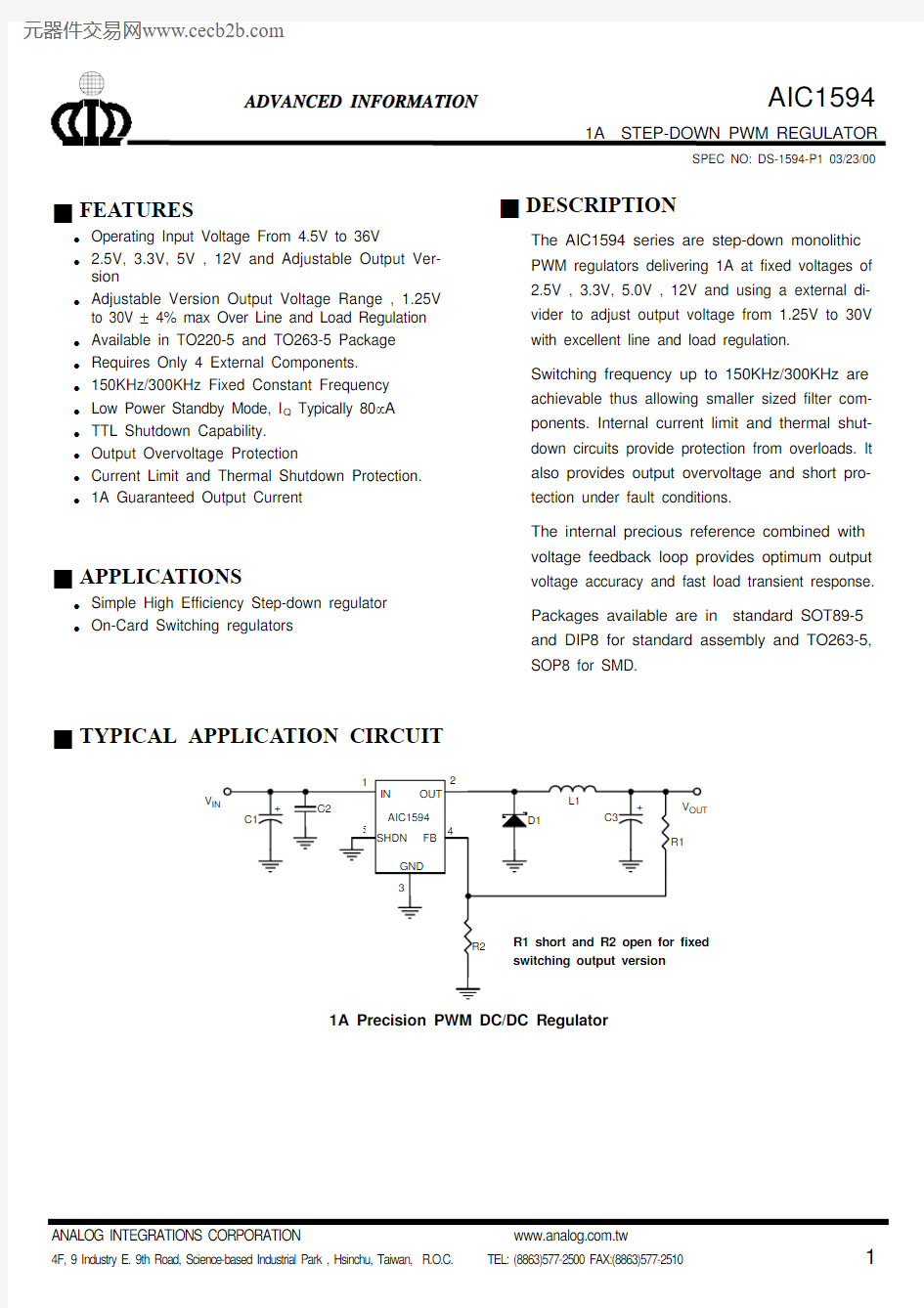
! TYPICAL APPLICATION CIRCUIT
V 1A Precision PWM DC/DC Regulator
SPEC NO: DS-1594-P1 03/23/00 !
Supply Voltage ……………..……………......……………............…………….................36V
FB, SHDN Pin Input Voltage……………..……………......…………………….................25V
Operating Temperature Range…….…………...............…………….………....... 0°C ~ 70°C
Storage Temperature Range……...................……..…….…………………. –65°C ~ 150°C
!TEST CIRCUIT
Refer to Typical Application Circuit.
SPEC NO: DS-1594-P1 03/23/00 !ELECTRICAL CHARACTERISTICS (T J=25°C, V IN=18V)
PARAMETER TEST CONDITIONS MIN.TYP.MAX.UNIT Input Voltage 4.536V Fixed Output Voltage
AIC1594-25 (V IN > 4.5V) 2.5V
AIC1594-33 (V IN > 4.5V) 3.3V
AIC1594-50 (V IN > 7.0V ) 5.0V
AIC1594-12 (V IN > 15V )12.0V Feedback Voltage AIC1594 Adjustable 1.25V Output Voltage Regulation4% Quiescent Current Internal switch off15mA Shutdown Quiescent Current SHDN = 5V (OFF)80μA Logic Input High(Regulator OFF)2V Logic Input Low(Regulator ON )0.8V Oscillator Frequency AIC1594A series150
Oscillator Frequency AIC1594B series300KHz Output Current Limit 1.0 1.5A Over Voltage Protection120% Maximum Duty Cycle100% Efficiency Vo=5V , Io=2A90%
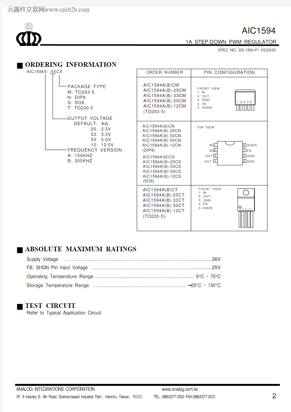
SPEC NO: DS-1594-P1 03/23/00 !PIN DESCRIPTIONS
TO-220-5, TO-263-5
PIN 1: IN Supply voltage input for the IC
switching regulator. A suitable input
bypass capacitor must be present at
this pin to minimize voltage transients
and to supply the switching currents
needed by the regulator.
PIN 2:OUT Internal switch. The voltage at this pin
switches between ( V IN-V SAT) and
approximately –0.5V, with a duty cycle
of approximately V OUT/V IN.
PIN 3: GND Ground requires a short, low noise
connection to ensure good load
regulation.PIN 4: FB Feedback input for fixed-output or
adjustable-output version. Connect di-
rectly to output for fixed operation
version or to a resistor divider for ad-
justable operation versions.
PIN 5:SHDN Allows the switching regulator circuit
to be shutdown using logic level sig-
nals thus dropping the total input sup-
ply current to approximately 80μA.
Drive it high to disable the reference ,
control circuitry , and internal
switches .Drive low or connect to
GND for normal operation.
SO8, DIP8
PIN 1, 2:IN Supply voltage input for the IC switch-
ing regulator. A suitable input bypass
capacitor must be present at this pin to
minimize voltage transients and to
supply the switching currents needed
by the regulator.
PIN 3, 4:OUT Internal switch. The voltage at this pin
switches between ( V IN-V SAT) and ap-
proximately –0.5V, with a duty cycle of
approximately V OUT/VIN.
PIN 5, 6: GNDGround requires a short, low noise
connection to ensure good load regu-
lation.PIN 7: FB Feedback input for fixed-output or ad-
justable-output version. Connect di-
rectly to output for fixed operation ver-
sion or to a resistor divider for adjusta-
ble operation versions.
PIN 8:SHDN Allows the switching regulator cir-
cuit to be shutdown using logic level
signals thus dropping the total input
supply current to approximately 80μA.
Drive it high to disable the reference ,
control circuitry , and internal
switches .Drive low or connect to GND
for normal operation.
SPEC NO: DS-1594-P1 03/23/00
! BLOCK DIAGRAM
IN
FB
! PHYSICAL DIMENSIONS
" 8 LEAD PLASTIC SO (unit: mm)
SYMBOL
MIN MAX A
1.35 1.75A10.100.25B 0.330.51C 0.190.25D 4.80 5.00E
3.80
4.00e 1.27(TYP)
H 5.80 6.20L
0.40
1.27
SPEC NO: DS-1594-P1 03/23/00
" 8 LEAD PLASTIC DIP (unit: mm)
SYMBOL MIN MAX A1
0.381—A2 2.92 4.96b 0.350.56C
0.200.36D 9.0110.16E
7.628.26E1 6.097.12e 2.54 (TYP)
eB —10.92L
2.92
3.81