
Silicon Phototransistor and Photo Darlington in Miniature 0805 SMD Package
OP500, OP501, OP500DA, OP501DA
Description:
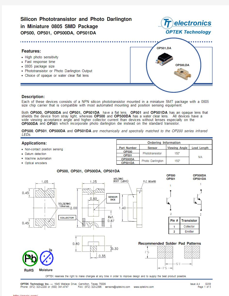
Each of these devices consists of a NPN silicon phototransistor mounted in a miniature SMT package with a 0805 size chip carrier that is compatible with most automated mounting and position sensing equipment.
Both OP500, OP500DA and OP501, OP501DA have a flat lens. OP501 and OP501DA has an opaque lens that shields the device from stray light, whereas OP500 and OP500DA has a water clear lens. All devices have a wide viewing acceptance angle and higher collector current than devices without lenses especially on the OP500DA and OP501 which incorporate photo darlington die instead on the standard transistor.
OP500, OP501, OP500DA and OP501DA are mechanically and spectrally matched to the OP200 series infrared LEDs.
Applications:
? Non-contact position sensing ? Datum detection ? Machine automation ? Optical encoders
Ordering Information
Part Number Sensor Viewing Angle
Lead Length
OP500 Phototransistor 150°
N/A
OP501 OP500DA Photo Darlington
150°
OP501DA
OP500, OP501, OP500DA, OP501DA
OP500 OP501
OP500DA
OP501DA
Recommended Solder Pad Patterns
COLLECTOR
SENSOR DICE
RoHS Moisture
2a
Silicon Phototransistor and Photo Darlington
in Miniature 0805 SMD Package
OP500, OP501, OP500DA, OP501DA
Absolute Maximum Ratings (T A =25°C unless otherwise noted)
Storage Temperature Range -40o C to +100o C Operating Temperature Range -25o C to +85o C
Lead Soldering Temperature (1) 260° C Collector-Emitter Voltage
OP500, OP501
OP500DA, OP501DA 30 V 35 V Emitter-Collector Voltage 5 V Power Dissipation (2) OP500, OP501
OP500DA, OP501DA
75 mW 100 mW
Collector Current OP500, OP501
OP500DA, OP501DA 20 mA 32 mA Notes:
1. Solder time less than 5 seconds at temperature extreme.
2. Derate linearly at 2.17 mW/° C above 25° C.
3. Light source is an unfiltered GaAs LED with a peak emission wavelength of 935 nm and a radiometric intensity level which varies less
than 10% over the entire lens surface of the phototransistor being tested.
4. To calculate typical collector dark current in μA, use the formulate I CEO = 10(0.04 t - ?), where T A is the ambient temperature in ° C.
Electrical Characteristics (T A = 25°C unless otherwise noted)
SYMBOL PARAMETER MIN TYP MAX UNITS TEST CONDITIONS Input Diode I C(ON)
On-State Collector Current
OP500, OP501
OP500DA, OP501DA
0.1 10.0 - - - - mA
V CE = 5.0 V, E E = 0.15 mW/cm 2 (3) V CE = 5.0 V, E E = 0.15 mW/cm 2 (3) V CE(SAT) Collector-Emitter Saturation Voltage OP500, OP501
OP500DA, OP501DA - - - - 0.3 1.0 V
I C = 100 μA, E E = 1.0 mW/cm 2 (3) I C = 1 mA, E E = 0.15 mW/cm 2 (3) I CEO Collector-Emitter Dark Current - -
100
nA
V CC = 5.0 V (4)
V BR(CEO)
Collector-Emitter Breakdown Voltage OP500, OP501
OP500DA, OP501DA
30 35 - - V I C = 100 μA, E E = 0 V BR(ECO)
Emitter-Collector Breakdown Voltage OP500, OP501 OP500DA, OP501DA 5 5
- - - - V
I E = 100 μA, E E = 0 I C = 100 μA, E E = 0 t r, t f Rise and Fall Times OP500, OP501
OP500DA, OP501DA
- 15 50
- 60
μs
I C = 1 mA, R L = 1K ? I C = 1 mA, R L = 1K ?
Silicon Phototransistor and Photo Darlington
in Miniature 0805 SMD Package
OP500, OP501, OP500DA, OP501DA
OP500, OP501
-25
Temperature—(°C)
C o l l e c t o r -E m i t t e r
D a r k C u r r e n t (n A )
I C (O N ) - O n -S t a t e C o l l e c t o r C u r r e n t (m A )
0 1 2 3 4 5
Collector-Emitter Voltage (V)
Relative On-State Collector Current –
Ic (mA)
vs. Collector-Emitter Voltage—V CE (V)
Collector-Emitter Dark Current
vs. Temperature-T A
Silicon Phototransistor and Photo Darlington
in Miniature 0805 SMD Package
OP500, OP501, OP500DA, OP501DA
OP500, OP501
R e l a t i v e C o l l e c t o r C u r r e n t
Relative On-State Collector Current
vs. Irradiance—Ee (mW/cm 2)
0 1.0 2.0 3.0 4.0 Ee—Irradiance (mW/cm 2)
R e l a t i v e C o l l e c t o r C u r r e n t
Relative On-State Collector Current-IC (mA)
vs. Temperature-T A
5.0
6.0
7.0
8.0
OP500DA, OP501DA
Collector-Emitter Dark Current
vs. Temperature-T A
-25
Temperature—(°C)
C o l l e c t o r -E m i t t e r
D a r k C u r r e n t (n A )
I C (O N ) - O n -S t a t e C o l l e c t o r C u r r
e n t (m A )
Relative On-State Collector Current –
Ic (mA)
vs. Collector-Emitter Voltage—V CE (V)
0 0.5 1.0 1.5 2.5 3
Collector-Emitter Voltage (V)
Silicon Phototransistor and Photo Darlington in Miniature 0805 SMD Package
OP500, OP501, OP500DA, OP501DA
R e l a t i v e C o l l e c t o r C u r r e n t —%
0 0.50
1.0
Irradiance- Ee(mW/cm 2)
R e l a t i v e C o l l e c t o r C u r r e n t —%
1.5
2.0
OP500DA, OP501DA
Relative On-State Collector Current
vs. Irradiance—Ee (mW/cm 2)
Relative On-State Collector Current-IC (mA)
分销商库存信息:
OPTEK-TECHNOLOGY
OP501OP500DA OP500 OP501DA