AT89C51的概况
1 AT89C51应用
单片机广泛应用于商业:诸如调制解调器,电动机控制系统,空调控制系统,汽车发动机和其他一些领域。这些单片机的高速处理速度和增强型外围设备集合使得它们适合于这种高速事件应用场合。然而,这些关键应用领域也要求这些单片机高度可靠。健壮的测试环境和用于验证这些无论在元部件层次还是系统级别的单片机的合适的工具环境保证了高可靠性和低市场风险。Intel 平台工程部门开发了一种面向对象的用于验证它的AT89C51 汽车单片机多线性测试环境。这种环境的目标不仅是为AT89C51 汽车单片机提供一种健壮测试环境,而且开发一种能够容易扩展并重复用来验证其他几种将来的单片机。开发的这种环境连接了AT89C51。本文讨论了这种测试环境的设计和原理,它的和各种硬件、软件环境部件的交互性,以及如何使用AT89C51。
1.1 介绍
8 位AT89C51 CHMOS 工艺单片机被设计用于处理高速计算和快速输入/输出。MCS51 单片机典型的应用是高速事件控制系统。商业应用包括调制解调器,电动机控制系统,打印机,影印机,空调控制系统,磁盘驱动器和医疗设备。汽车工业把MCS51 单片机用于发动机控制系统,悬挂系统和反锁制动系统。AT89C51 尤其很好适用于得益于它的处理速度和增强型片上外围功能集,诸如:汽车动力控制,车辆动态悬挂,反锁制动和稳定性控制应用。由于这些决定性应用,市场需要一种可靠的具有低干扰潜伏响应的费用-效能控制器,服务大量时间和事件驱动的在实时应用需要的集成外围的能力,具有在单一程序包中高出平均处理功率的中央处理器。拥有操作不可预测的设备的经济和法律风险是很高的。一旦进入市场,尤其任务决定性应用诸如自动驾驶仪或反锁制动系统,错误将是财力上所禁止的。重新设计的费用可以高达500K 美元,如果产品族享有同样内核或外围设计缺陷的话,费用会更高。另外,部件的替代品领域是极其昂贵的,因为设备要用来把模块典型地焊接成一个总体的价值比各个部件高几倍。为了缓和这些问题,在最坏的环境和电压条件下对这些单片机进行无论在部件级别还是系统级别上的综合测试是必需的。Intel Chandler 平台工程组提供了各种单片机和处理器的系统验证。这种系统的验证处理可以被分解为三个主要部分。系统的类型和应用需求决定了能够在设备上执行的测试类型。
1.2 AT89C51提供以下标准功能:
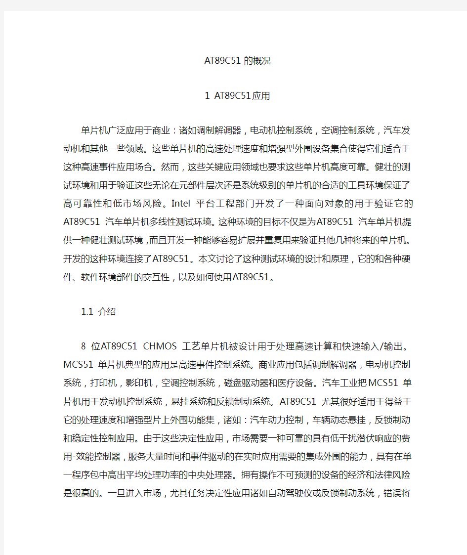
4k 字节FLASH 闪速存储器,128 字节内部RAM,32 个I/O 口线,2 个16 位定时/计数器,一个5 向量两级中断结构,一个全双工串行通信口,片内振荡器及时钟电路。同时,AT89C51 降至0Hz 的静态逻辑操作,并支持两种可选的节电工作模式。空闲方式体制CPU 的工作,但允许RAM,定时/计数器,串行通信口及中断系统继续工作。掉电方式保存RAM 中的内容,但振荡器体制工作并禁止其他所有不见工作直到下一个硬件复位。
图1-2-1 AT89C51 方框图
1.3引脚功能说明
·Vcc:电源电压
·GND:地
·P0 口:P0 口是一组8 位漏极开路型双向I/O 口,也即地址/数据总线复用。作为输出口用时,每位能吸收电流的方式驱动8 个TTL 逻辑门电路,对端口写“1”可作为高阻抗输入端用。在访问外部数据存储器或程序存储器时,这组口线分时转换地址(低8 位)和数据总线复用,在访问期间激活内部上拉电阻。在Flash 编程时,P0 口接受指令字节,而在程序校验时,输出指令字节,校验时,要求外接上拉电阻。
·P1 口:P1 是一个带内部上拉电阻的8 位双向I/O 口,P1 的输出缓冲级可驱动(吸收或输出电流)4 个TTL 逻辑门电路。对端口写“1”,通过内部的上拉电阻把端口拉到高电平,此时可作输入口。作为输入口使用时,因为内部存在上拉电阻,某个引脚被外部信号拉低时会输出一个电流(IIL)。Flash 编程和程序校验期间,P1 接受低8 位地址。
·P2 口:P2 是一个带有内部上拉电阻的8 位双向I/O 口,P2 的输出缓冲级可驱动(吸收或输出电流)4 个TTL 逻辑门电路。对端口写“1”,通过内部的上拉电阻把端口拉到高电平,此时可作输入口。作为输入口使用时,因为内部存在上拉电阻,某个引脚被外部信号拉低时会输出一个电流(IIL)。在访问外部程序存储器或16 位四肢的外部数据存储器(例如执行MOVX @DPTR指令)时,P2 口送出高8 位地址数据,在访问8 位地址的外部数据存储器(例如执行MOVX @ RI 指令)时,P2 口线上的内容(也即特殊功能寄存器(SFR)区中R2 寄存器的内容),在整个访问期间不改变。Flash 编程和程序校验时,P2 也接收高位地址和其他控制信号。
·P3 口:P3 是一个带有内部上拉电阻的8 位双向I/O 口,P3 的输出缓冲级可驱动(吸收或输出电流)4 个TTL 逻辑门电路。对端口写“1”,通过内部的上拉电阻把端口拉到高电平,此时可作输入口。作为输入口使用时,因为内部存在上拉电阻,某个引脚被外部信号拉低时会输出一个电流(IIL)。P3 口还接收一些用于Flash 闪速存储器编程和程序校验的控制信号。
·RST:复位输入。当振荡器工作时,RST 引脚出现两个机器周期以上高电平将使单片机复位。
·ALE/PROG:当访问外部程序存储器或数据存储器时,ALE(地址锁存允许)输出脉冲用于锁存地址的低8 位字节。即使不访问外部存储器,ALE 仍以时钟振荡频率的1/6 输出固定的正脉冲信号,因此它可对外输出时钟或用于定时目的。要注意的是,每当访问外部数据存储器时将跳过一个ALE 脉冲。对Flash 存储器编程期间,该引脚还用于输入编程脉冲(PROG)。如有必要,可通过对特殊功能寄存器(SFR)区中的8EH 单元D0 位置位,可禁止ALE 操作。该位置位后,只有一条MOVX 和MOVC 指令ALE 才会被激活。此外,该引脚会被微
弱拉高,单片机执行外部程序时,应设置ALE 无效。
·PSEN:程序存储允许输出是外部程序存储器的读选通型号,当89C51 由外部存储器取指令(或数据)时,每个机器周期两次PSEN 有效,即输出两个脉冲。在此期间,当访问外部数据存储器,这两次有效的PSEN 信号不出现。
·EA/VPP:外部访问允许。欲使CPU 仅访问外部程序存储器(地址为
0000H—FFFFH),EA 端必须保持低电平(接地)。需注意的是:如果加密位LB1 被编程,复位时内部会锁存EA 端状态。如EA 端为高电平(接Vcc 端),CPU 则执行内部程序存储器中的指令。Flash 存储器编程时,该引脚加上+12v 的编程允许电源Vpp,当然这必须是该器件使用12v 编程电压Vpp。
·XTAL1:振荡器反相放大器及内部时钟发生器的输入端。
·XTAL2:振荡器反相放大器的输出端。89C51 中有一个用于构成内部振荡器的高增益反相放大器,引脚XTAL1 和XTAL2分别是该放大器的输入端和输出端。这个放大器与作为反馈元件的片外石英晶体或陶瓷谐振器一起构成自激振荡器,振荡电路参见图5。外接石英晶体或陶瓷谐振器及电容C1、C2 接在放大器的反馈回路中构成并联振荡电路。对电容C1、C2 虽没有十分严格的要求,但电容容量的大小会轻微影响振荡频率的高低、振荡器工作的稳定性、起振的难易程度及温度稳定性,如果使用石英晶体,我们推荐电容使用30Pf±10 Pf,而如使用陶瓷谐振器建议选择40Pf±10Pf。用户也可以采用外部时钟。这种情况下,外部时钟脉冲接到XTAL1 端,即内部时钟发生器的输入端XTAL2 则悬空。
·掉电模式:
在掉电模式下,振荡器停止工作,进入掉电模式的指令是最后一条被执行的指令,片内RAM 和特殊功能寄存器的内容在终止掉电模式前被冻结。推出掉电模式的唯一方法是硬件复位,复位后将重新定义全部特殊功能寄存器但不改变RAM 中的内容,在Vcc 恢复到正常工作电平前,复位应无效,且必须保持一定时间以使振荡器重启动并稳定工作。89C51 的程序存储器阵列是采用字节写入方式编程的,每次写入一个字符,要对整个芯片的EPROM 程序存储器写入一个非空字节,必须使用片擦除的方法将整个存储器的内容清楚。
2 编程方法
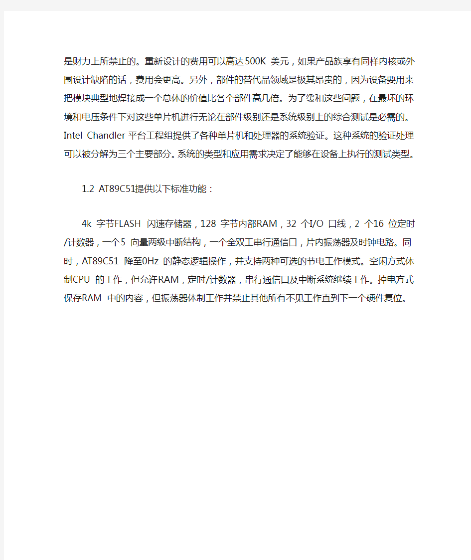
编程前,设置好地址、数据及控制信号,编程单元的地址加在P1 口和P2 口的P2.0—P2.3(11 位地址范围为0000H——0FFFH),数据从P0口输入,引脚P2.6、P2.7 和P3.6、P3.7 的电平设置见表6,PSEB 为低电平,RST保持高电平,EA/Vpp 引脚是编程电源的输入端,按要求加上编程电压,ALE/PROG引脚输入编程脉冲(负脉冲)。编程时,可采用4—20MHz 的时钟振荡器,89C51 编程方法如下:在地址线上加上要编程单元的地址信号在数据线上加上要写入的数
据字节。激活相应的控制信号。在高电压编程方式时,将EA/Vpp 端加上+12v 编程电压。每对Flash 存储阵列写入一个字节或每写入一个程序加密位,加上一个ALE/PROG 编程脉冲。改变编程单元的地址和写入的数据,重复1—5 步骤,知道全部文件编程结束。每个字节写入周期是自身定时的,通常约为1.5ms。·数据查询89C51 单片机用数据查询方式来检测一个写周期是否结束,在一个写周期中,如需要读取最后写入的那个字节,则读出的数据的最高位(P0.7)是原来写入字节的最高位的反码。写周期开始后,可在任意时刻进行数据查询。
2.1Ready/Busy:
字节编程的进度可通过Ready/Busy 输出信号检测,编程期间,ALE 变为高电平“H”后P3.4(Ready/Busy)端被拉低,表示正在编程状态(忙状态)。编程完成后,P3.4 变为高电平表示准备就绪状态。
·程序校验:如果加密位LB、LB2 没有进行编程,则代码数据可通过地址和数据线读回原编写的数据,采用下图的电路,程序存储器的地址由P1 口和P2 口的P2.0—P2.3 输入,数据由P0 口读出,P206、P2.7 和P3.6、P3.7 的控制信号见表6,PSEN 保持低电平,ALE、EA 和RST 保持高电平。校验时,P0 口必须接上10k 左右的上拉电阻。
图2-1-1 编程电路图2-2-2 校验电路
2.2芯片擦除:
利用控制信号的正确组合(表6)并保持ALE/PROG 引脚10ms 的低电平脉冲宽度即可将EPROM 阵列(4k 字节)和三个加密位整片擦除,代码阵列在片擦除操作中将任何非空单元写入”1”,这步骤需在编程之前进行。
2.3读片内签名字节:
89C51 单片机内有3 个签名字节,地址为030H、031H 和032H。于声明该器件的厂商、号和编程电压。读签名字节的过程和单元030H、031H 和032H的正常校验相仿,只需要将P3.6 和P3.7 保持低电平,返回值意义如下:(030H) = 1EH 声明产品由ATMEL 公司制造。
(031H) = 51H 声明为89C51 单片机。
(032H) = FFH 声明为12V 编程电压。
(032H) = 05H 声明为5 编程电压。
2.4 编程接口:
采用控制信号的正确组合可对Flash 闪速存储阵列中的每一代码字节进行写入和存储器的整片擦除,写操作周期是自身定时的,初始化后它将自动定时到操作完成。微机接口实现两种信息形式的交换。在计算机之外,由电子系统所处理的信息以一种物理信号形式存在,但在程序中,它是用数字表示的。任一接口的功能都可分为以某种形式进行数据库变换的一些操作,所以外部和内部形式的转换是由许多步骤完成的。模拟-数字转换器(ADC)用来将连续变化信号变成相应的数字量,这数字量可是可能性的二进制数值中的一固定值。如果传感器输出不是连续变化的,就不需模拟-数字转换。这种情况下,信号调理单元必须将输入信号变换成为另一信号,也可直接与接口的下一部分,即微计算机本身的输入输出单元相连接。输出接口采用相似的形式,明显的差别在于信息流的方向相反;是从程序到外部世界。这种情况下,程序可称为输出程序,它监督接口的操作并完成数字-模拟转换器(DAC)所需数字的标定。该子程序依次送出信息给输出器件,产生相应的电信号,由DAC 转换成模拟形式。最后,信号经调理(通常是放大)以形成适应于执行器操作的形式。在微机电路中使用的信号几乎总是太小而不能被直接地连到“外部世界”,因而必须用某种形式将其转换成更适宜的形式。接口电路部分的设计是使用微机的工程师所面临最重要的任务之一。我们已经了解到微机中,信号以离散的位形式表示。当微机要与只有打开或关闭操作的设备相连时,这种数字形式是最有用的,这里每一位都可表示一开关或执行器的状态。为了解决实际问题,一个单片机不仅包括CPU,程序和数据存储器,另外,它必须含有通过CPU 访问外部信息的硬件。一旦CPU 收集到数据信息和流程,它必须能够改变外部领域的一部分,这些硬件设备称作外围设备,它们是CPU 通往外部的窗口。
单片机可利用外围设备中最基本的用于一般用途的I/O 接口,每个I/O 接口既可作为输入端又可作为输出端,每个I/O 接口的功能取决与程序初始化阶段对数据方位寄存器相应位进行置一和清零操作,通过CPU 指令对数据寄存器相应位进行置一和清零来置一和清零输出端口,同样输入端口逻辑位也可以通过CPU 指
令访问。一些类型的串行口单元允许CPU 与外部设备进行串口通信,用串口位代替平行位进行通信需要少许的I/O 口,这样使通信费用降低但速度也相对慢些。串口传送可以同步也可以异步。
The General Situation of A T89C51
Chapter 1 The application of A T89C51 Microcontrollers are used in a multitude of commercial applications such as modems, motor-control systems, air conditioner control systems, automotive engine and among others. The high processing speed and enhanced peripheral set of these microcontrollers make them suitable for such high-speed event-based applications. However, these critical application domains also require that these microcontrollers are highly reliable. The high reliability and low market risks can be ensured by a robust testing process and a proper tools environment for the validation of these microcontrollers both at the component and at the system level. Intel Plaform Engineering department developed an object-oriented multi-threaded test environment for the validation of its AT89C51 automotive microcontrollers. The goals of thisenvironment was not only to provide a robust testing environment for the AT89C51 automotive microcontrollers, but to develop an environment which can be easily extended and reused for the validation of several other future microcontrollers. The environment was developed in conjunction with Microsoft Foundation Classes (AT89C51). The paper describes the design and mechanism of this test environment, its interactions with various hardware/software environmental components, and how to use AT89C51.
1.1 Introduction
The 8-bit AT89C51 CHMOS microcontrollers are designed to handle high-speedcalculations and fast input/output operations. MCS 51 microcontrollers are typically used for high-speed event control systems. Commercial applications include modems,motor-control systems, printers, photocopiers, air conditioner control systems, disk drives,and medical instruments. The automotive industry use MCS 51 microcontrollers in engine-control systems, airbags, suspension systems, and antilock braking systems (ABS). The AT89C51 is especially well suited to applications that benefit from its processing speed and enhanced on-chip peripheral functions set, such as automotive power-train control, vehicle dynamic suspension, antilock braking, and stability control applications. Because of these critical applications, the market requires a reliable cost-effective controller with a low interrupt latency response, ability to service the high number of time and event driven integrated peripherals
needed in real time applications, and a CPU with above average processing power in a single package. The financial and legal risk of having devices that operate unpredictably is very high. Once in the market, particularly in mission criticalapplications such as an autopilot or anti-lock braking system, mistakes are financiallyprohibitive. Redesign costs can run as high as a $500K, much more if the fix means 2 back annotating it across a product family that share the same core and/or peripheral design flaw. In addition, field replacements of components is extremely expensive, as the devices are typically sealed in modules with a total value several times that of the component. To mitigate these problems, it is essential that comprehensive testing of the controllers be carried out at both the component level and system level under worst case environmental and voltage cond itions.This complete and thorough validation necessitates not only a well-defined process but also a proper environment and tools to facilitate and execute the mission successfully.Intel Chandler Platform Engineering group provides post silicon system validation (SV) of various micro-controllers and processors. The system validation process can be broken into three major parts.The type of the device and its application requirements determine which types of testing are performed on the device.
1.2 The AT89C51 provides the following standard features:
4Kbytes of Flash, 128 bytes of RAM, 32 I/O lines, two 16-bittimer/counters, a five vector two-level interrupt architecture,a full duple ser -ial port, on-chip oscillator and clock circuitry.In addition, the AT89C51 is designed with static logic for operation down to zero frequency and supports two software selectable power saving modes. The Idle Mode stops the CPU while allowing the RAM, timer/counters,serial port and interrupt sys -tem to continue functioning. The Power-down Mode saves the RAM contents but freezes the oscil –lator disabling all other chip functions until the next hardware reset.
Figure 1-2-1Block Diagram 1-3Pin Description
VCC Supply voltage.
GND Ground.
Port 0:Port 0 is an 8-bit open-drain bi-directional I/O port. As an output port, each pin cansink eight TTL inputs. When 1s are written to port 0 pins, the pins can be used as highimpedance inputs.Port 0 may also be configured to be the multiplexed loworder address/data busduring accesses to external program and data memory. In this mode P0 has internalpullups.Port 0 also receives the code bytes during Flash programming,and outputs the codebytes during program verification. External pullups are required during programverification.
Port 1:Port 1 is an 8-bit bi-directional I/O port with internal pullups.The Port 1 output buffers can sink/so -urce four TTL inputs.When 1s are written to Port 1 pins they are pulled high by the internal pullups and can be used as inputs. As inputs, Port 1 pins that are externally being pulled low will source current (IIL) because of the internal pullups.Port 1 also receives the low-order address bytes during Flash programming and verification.
Port 2:Port 2 is an 8-bit bi-directional I/O port with internal pullups.The Port 2 outputbuffers can sink/source four TTL inputs.When 1s are written to Port 2 pins they arepulled high by the internal pullups and can be used as inputs. As inputs, Port 2 pins that are externally being pulled low will source current (IIL) because of the internal pullups. Port 2 emits the high-order address byte during fetches from external program memory and during accesses to Port 2 pins that are externally being pulled low will source current (IIL) because of the internal pullups.Port 2 emits the high-order address byte during fetches from external program memory and during accesses to external data memory that use 16-bit addresses (MOVX@DPTR). In this application, it uses strong internal pull-ups when emitting 1s. During accesses to external data memory that use 8-bit addresses (MOVX @ RI), Port 2 emits the contents of the P2 Special Function Register.Port 2 also receives the high-order address bits and some control signals durin Flash programming and verification.
Port 3:Port 3 is an 8-bit bi-directional I/O port with internal pullups.The Port 3 outputbuffers can sink/sou -rce four TTL inputs.When 1s are written to Port 3 pins they are pulled high by the internal pullups and can be used as inputs. As inputs,Port 3 pins that are externally being pulled low will source current (IIL) because of the pullups.
Port 3 also serves the functions of various special featuresof the AT89C51 as listed below:
RST:Reset input. A high on this pin for two machine cycles while the oscillator
is running resets the device.
ALE/PROG:Address Latch Enable output pulse for latching the low byte of the address duringaccesses to external memory.This pin is also the program pulse input (PROG) during Flash programming.In normal operation ALE is emitted at a constant rate of 1/6 the oscillator frequency,and may be used for external timing or clocking purposes. Note, however, that one ALEpulse is skipped duri -ng each access to external DataMemory.If desired, ALE operationcan be disabled by setting bit 0 of SFR location 8EH. With the bit set, ALE is active onlyduring a MOVX or MOVC instruction. Otherwise, the pin is weakly pulled high. Settingthe ALE-disable bit has no effect if the microcontroller is in external execution mode.
PSEN:Program Store Enable is the read strobe to external program memory. When theAT89C51 is executing code from external program memory, PSEN is activated twiceeach machine cycle, except that two PSEN activations are skipped during each access toexternal data memory.
EA/VPP:External Access Enable. EA must be strapped to GND in order to enable the deviceto fetch code from external program memory locations starting at 0000H up to FFFFH.Note, however, that if lock bit 1 is programmed, EA will be internally latched onreset.EA should be strapped to VCC for internal program executions. This pin alsreceives the 12-volt programming enable voltage (VPP) during Flash programming, forparts that require 12-volt VPP.
XTAL1:Input to the inverting oscillator amplifier and input to the internal clock operatingcircuit.
XTAL2:Output from the inverting oscillator amplifier.Oscillator CharacteristicsXTAL1 and XTAL2 are the input and output, respectively, of an inverting amplifierwhich can be configured for use as an on-chip oscillator, as shown in Figure 1. Either aquartz crystal or ceramic resonator may be used. To drive the device from an externalclock source, XTAL2 should be left unconnected while XTAL1 is driven as shown in Figure 2.There are no requirements on the duty cycle of the external clock signal, since the input to the internal clocking circuitry is through a divide-by-two flip-flop, but minimum and maximum voltage high and low time specifications must be observed.Idle Mode In idle mode, the CPU puts itself to sleep while all the onchip peripherals remain active. The mode is invoked by software. The content of the on-chip RAM and all the special functions registers remain unchanged during this mode. The idle mode can be terminated by any enabled interrupt or by a hardware reset. It should be noted that when idle is terminated by a hard ware reset,
the device normally resumes program execution,from where it left off, up to two machine cycles before the internal reset algorithm takes control. On-chip hardware inhibits access to internal RAM in this event, but access to the port pins is not inhibited. To eliminate the possibility of an unexpected write to a port pin when Idle is terminated by reset, the instruction following the one that invokes Idle should not be one that writes to a port pin or to external memory.
Power-down Mode
In the power-down mode, the oscillator is stopped, and the instruction that invokes power-down is the last instruction executed. The on-chip RAM and Special Function Registers retain their values until the power-down mode is terminated. The only exit from power-down is a hardware reset. Reset redefines the SFRs but does not change the on-chip RAM. The reset should not be activated before VCC is restored to its normal operating level and must be held active long enough to allow the oscillator to restart and stabilize.The AT89C51 code memory array is programmed byte-bybyte in either programming mode. To program any nonblank byte in the on-chip Flash Memory, the entire memory must be erased using the Chip Erase Mode.
2 Programming Algorithm
Before programming the AT89C51, the address, data and control signals should be set up according to the Flash programming mode table and Figure 3 and Figure 4. To program the AT89C51, take the following steps.1. Input the desired memory location on the address lines.2. Input the appropriate data byte on the data lines. 3. Activate the correct combination of control signals. 4. Raise EA/VPP to 12V for the high-voltage programming mode. 5. Pulse ALE/PROG once to program a byte in the Flash array or the lock bits. The byte-write cycle is self-timed and typically takes no more than 1.5 ms. Repeat steps 1 through 5, changing the address and data for the entire array or until the end of the object file is reached. Data Polling: The AT89C51 features Data Polling to indicate the end of a write cycle. During a write cycle, an attempted read of the last byte written will result in the complement of the written datum on PO.7. Once the write cycle has been completed, true data are valid on all outputs, and the next cycle may begin. Data Polling may begin any time after a write cycle has been initiated.
2.1Ready/Busy:
The progress of byte programming can also be monitored by the RDY/BSY output signal. P3.4 is pulled low after ALE goes high during programming to indicate
BUSY. P3.4 is pulled high again when programming is done to indicate READY.
Program Verify:
If lock bits LB1 and LB2 have not been programmed, the programmed code data can be read back via the address and data lines for verification. The lock bits cannot be verified directly. Verification of the lock bits is achieved by observing that their features are enabled.
Figure 2-1-1 Programming the Flash Figure 2-2-2 Verifying the Flash
2.2 Chip Erase:
The entire Flash array is erased electrically by using the proper combination of control signals and by holding ALE/PROG low for 10 ms. The code array is written with all “1”s. The chip erase operation must be executed before the code memory can be re-programmed.
2.3 Reading the Signature Bytes:
The signature bytes are read by the same procedure as a normal verification of locations 030H, 031H, and 032H, except that P3.6 and P3.7 must be pulled to a logic low. The values returned areas follows.
(030H) = 1EH indicates manufactured by Atmel
(031H) = 51H indicates 89C51
(032H) = FFH indicates 12V programming
(032H) = 05H indicates 5V programming
2.4 Programming Interface
Every code byte in the Flash array can be written and the entire array can be
erased by using the appropriate combination of control signals. The write operation cycle is selftimed and once initiated, will automatically time itself to completion. A microcomputer interface converts information between two forms. Outside the microcomputer the information handled by an electronic system exists as a physical signal, but within the program, it is represented numerically. The function of any interface can be broken down into a number of operations which modify the data in some way, so that the process of conversion between the external and internal forms is carried out in a number of steps. An analog-to-digital converter(ADC) is used to convert a continuously variable signal to a corresponding digital form which can take any one of a fixed number of possible binary values. If the output of the transducer does not vary continuously, no ADC is necessary. In this case the signal conditioning section must convert the incoming signal to a form which can be connected directly to the next part of the interface, the input/output section of the microcomputer itself. Output interfaces take a similar form, the obvious difference being that here the flow of information is in the opposite direction; it is passed from the program to the outside world. In this case the program may call an output subroutine which supervises the operation of the interface and performs the scaling numbers which may be needed for digital-to-analog converter(DAC). This subroutine passes information in turn to an output device which produces a corresponding electrical signal, which could be converted into analog form using a DAC. Finally the signal is conditioned(usually amplified) to a form suitable for operating an actuator.The signals used within microcomputer circuits are almost always too small to be connected directly to the outside world” and some kind of interface must be used to translate them to a more appropriate form. The design of section of interface circuits is one of the most important tasks facing the engineer wishing to apply microcomputers. We have seen that in microcomputers information is represented as discrete patterns of bits; this digital form is most useful when the microcomputer is to be connected to equipment which can only be switched on or off, where each bit might represent the state of a switch or actuator. To solve real-world problems, a microcontroller must have more than just a CPU, a program, and a data memory. In addition, it must contain hardware allowing the CPU to access information from the outside world. Once the CPU gathers information and processes the data, it must also be able to effect change on some portion of the outside world. These hardware devices, called peripherals, are the CPU’s window to the outside.
The most basic form of peripheral available on microcontrollers is the general
purpose I70 port. Each of the I/O pins can be used as either an input or an output. The function of each pin is determined by setting or clearing corresponding bits in a corresponding data direction register during the initialization stage of a program. Each output pin may be driven to either a logic one or a logic zero by using CPU instructions to pin may be viewed (or read.) by the CPU using program instructions. Some type of serial unit is included on microcontrollers to allow the CPU to communicate bit-serially with external devices. Using a bit serial format instead of bit-parallel format requires fewer I/O pins to perform the communication function, which makes it less expensive, but slower. Serial transmissions are performed either synchronously or asynchronously.
五、外文资料翻译 Stress and Strain 1.Introduction to Mechanics of Materials Mechanics of materials is a branch of applied mechanics that deals with the behavior of solid bodies subjected to various types of loading. It is a field of study that i s known by a variety of names, including “strength of materials” and “mechanics of deformable bodies”. The solid bodies considered in this book include axially-loaded bars, shafts, beams, and columns, as well as structures that are assemblies of these components. Usually the objective of our analysis will be the determination of the stresses, strains, and deformations produced by the loads; if these quantities can be found for all values of load up to the failure load, then we will have obtained a complete picture of the mechanics behavior of the body. Theoretical analyses and experimental results have equally important roles in the study of mechanics of materials . On many occasion we will make logical derivations to obtain formulas and equations for predicting mechanics behavior, but at the same time we must recognize that these formulas cannot be used in a realistic way unless certain properties of the been made in the laboratory. Also , many problems of importance in engineering cannot be handled efficiently by theoretical means, and experimental measurements become a practical necessity. The historical development of mechanics of materials is a fascinating blend of both theory and experiment, with experiments pointing the way to useful results in some instances and with theory doing so in others①. Such famous men as Leonardo da Vinci(1452-1519) and Galileo Galilei (1564-1642) made experiments to adequate to determine the strength of wires , bars , and beams , although they did not develop any adequate theo ries (by today’s standards ) to explain their test results . By contrast , the famous mathematician Leonhard Euler(1707-1783) developed the mathematical theory any of columns and calculated the critical load of a column in 1744 , long before any experimental evidence existed to show the significance of his results ②. Thus , Euler’s theoretical results remained unused for many years, although today they form the basis of column theory. The importance of combining theoretical derivations with experimentally determined properties of materials will be evident theoretical derivations with experimentally determined properties of materials will be evident as we proceed with
AT89C51外文翻译 Description The AT89C51 is a low-power, high-performance CMOS 8-bit microcomputer with 4K bytes of Flash Programmable and Erasable Read Only Memory (PEROM). The device is manufactured using Atmel’s high density nonvolatile memory technology and is compatible with the industry standard MCS-51? instruction-set and pinout. The on-chip Flash allows the program memory to be reprogrammed in-system or by a conventional nonvolatile memory programmer. By combining a versatile 8-bit CPU with Flash on a monolithic chip, the Atmel AT89C51 is a powerful microcomputer which provides a highly flexible and cost effective solution to many embedded control applications. Features ? Compatible with MCS-51? Products ? 4K Bytes of In-System Reprogrammable Flash Memory – Endurance: 1,000 Write/Erase Cycles ? Fully Static Operation: 0 Hz to 24 MHz ? Three-Level Program Memory Lock ? 128 x 8-Bit Internal RAM ? 32 Programmable I/O Lines ? Two 16-Bit Timer/Counters ? Six Interrupt Sources ? Programmable Serial Channel ? Low Power Idle and Power Down Modes The AT89C51 provides the following standard features: 4K bytes of Flash,128 bytes of RAM, 32 I/O lines, two 16-bit timer/counters, a five vector two-level interrupt architecture, a full duplex serial port, on-chip oscillator and clock circuitry. In addition, the AT89C51 is designed with static logic for operation down to zero frequency and supports two software selectable power saving modes. The Idle Mode stops the CPU while allowing the RAM, timer/counters, serial port and interrupt system to continue functioning. The Power-down Mode saves the RAM contents but freezes the oscillator disabling all other chip functions until the next hardware reset.
外文文献: Knowledge of the stepper motor What is a stepper motor: Stepper motor is a kind of electrical pulses into angular displacement of the implementing agency. Popular little lesson: When the driver receives a step pulse signal, it will drive a stepper motor to set the direction of rotation at a fixed angle (and the step angle). You can control the number of pulses to control the angular displacement, so as to achieve accurate positioning purposes; the same time you can control the pulse frequency to control the motor rotation speed and acceleration, to achieve speed control purposes. What kinds of stepper motor sub-: In three stepper motors: permanent magnet (PM), reactive (VR) and hybrid (HB) permanent magnet stepper usually two-phase, torque, and smaller, step angle of 7.5 degrees or the general 15 degrees; reaction step is generally three-phase, can achieve high torque output, step angle of 1.5 degrees is generally, but the noise and vibration are large. 80 countries in Europe and America have been eliminated; hybrid stepper is a mix of permanent magnet and reactive advantages. It consists of two phases and the five-phase: two-phase step angle of 1.8 degrees while the general five-phase step angle of 0.72 degrees generally. The most widely used Stepper Motor. What is to keep the torque (HOLDING TORQUE) How much precision stepper motor? Whether the cumulative: The general accuracy of the stepper motor step angle of 3-5%, and not cumulative.
在广州甚至广东的住宅小区电气设计中,一般都会涉及到小区的高低压供配电系统的设计.如10kV高压配电系统图,低压配电系统图等等图纸一大堆.然而在真正实施过程中,供电部门(尤其是供电公司指定的所谓电力设计小公司)根本将这些图纸作为一回事,按其电脑里原有的电子档图纸将数据稍作改动以及断路器按其所好换个厂家名称便美其名曰设计(可笑不?),拿出来的图纸根本无法满足电气设计的设计意图,致使严重存在以下问题:(也不知道是职业道德问题还是根本一窍不通) 1.跟原设计的电气系统货不对板,存在与低压开关柜后出线回路严重冲突,对实际施工造成严重阻碍,经常要求设计单位改动原有电气系统图才能满足它的要求(垄断的没话说). 2.对消防负荷和非消防负荷的供电(主要在高层建筑里)应严格分回路(从母线段)都不清楚,将消防负荷和非消防负荷按一个回路出线(尤其是将电梯和消防电梯,地下室的动力合在一起等等,有的甚至将楼顶消防风机和梯间照明合在一个回路,以一个表计量). 3.系统接地保护接地型式由原设计的TN-S系统竟曲解成"TN-S-C-S"系统(室内的还需要做TN-C,好玩吧?),严格的按照所谓的"三相四线制"再做重复接地来实施,导致后续施工中存在重复浪费资源以及安全隐患等等问题.. ............................(违反建筑电气设计规范等等问题实在不好意思一一例举,给那帮人留点混饭吃的面子算了) 总之吧,在通过图纸审查后的电气设计图纸在这帮人的眼里根本不知何物,经常是完工后的高低压供配电系统已是面目全非了,能有百分之五十的保留已经是谢天谢地了. 所以.我觉得:住宅建筑电气设计,让供电部门走!大不了留点位置,让他供几个必需回路的电,爱怎么折腾让他自个怎么折腾去.. Guangzhou, Guangdong, even in the electrical design of residential quarters, generally involving high-low cell power supply system design. 10kV power distribution systems, such as maps, drawings, etc. low-voltage distribution system map a lot. But in the real implementation of the process, the power sector (especially the so-called power supply design company appointed a small company) did these drawings for one thing, according to computer drawings of the original electronic file data to make a little change, and circuit breakers by their the name of another manufacturer will be sounding good design (ridiculously?), drawing out the design simply can not meet the electrical design intent, resulting in a serious following problems: (do not know or not know nothing about ethical issues) 1. With the original design of the electrical system not meeting board, the existence and low voltage switchgear circuit after qualifying serious conflicts seriously hinder the actual construction, often require changes to the original design unit plans to meet its electrical system requirements (monopoly impress ). 2. On the fire load and fire load of non-supply (mainly in high-rise building in) should be strictly sub-loop (from the bus segment) are not clear, the fire load and fire load of non-qualifying press of a circuit (especially the elevator and fire elevator, basement, etc.
at89c52单片机简介 中英文资料对照外文翻译文献综述 A T89C52 Single-chip microprocessor introduction Selection of Single-chip microprocessor 1. Development of Single-chip microprocessor The main component part of Single-chip microprocessor as a result of by such centralize to be living to obtain on the chip,In immediate future middle processor CPU。Storage RAM immediately﹑memoy read ROM﹑Interrupt system、Timer /'s counter along with I/O's rim electric circuit awaits the main microcomputer section,The lumping is living on the chip。Although the Single-chip microprocessor r is only a chip,Yet through makes up and the meritorous service be able to on sees,It had haveed the calculating machine system property,calling it for this reason act as Single-chip microprocessor r minisize calculating machine SCMS and abbreviate the Single-chip microprocessor。 1976Year the Inter corporation put out 8 MCS-48Set Single-chip microprocessor computer,After being living more than 20 years time in development that obtain continuously and wide-ranging application。1980Year that corporation put out high performance MCS -51Set Single-chip microprocessor。This type of Single-chip microprocessor meritorous service capacity、The addressing range wholly than early phase lift somewhat,Use also comparatively far more at the moment。1982Year that corporation put out the taller 16 Single-chip microprocessor MCS of performance once
International Journal of Minerals, Metallurgy and Materials Volume 17, Number 4, August 2010, Page 500 DOI: 10.1007/s12613-010-0348-y Corresponding author: Zhuan Li E-mail: li_zhuan@https://www.doczj.com/doc/d714776031.html, ? University of Science and Technology Beijing and Springer-Verlag Berlin Heidelberg 2010 Preparation and properties of C/C-SiC brake composites fabricated by warm compacted-in situ reaction Zhuan Li, Peng Xiao, and Xiang Xiong State Key Laboratory of Powder Metallurgy, Central South University, Changsha 410083, China (Received: 12 August 2009; revised: 28 August 2009; accepted: 2 September 2009) Abstract: Carbon fibre reinforced carbon and silicon carbide dual matrix composites (C/C-SiC) were fabricated by the warm compacted-in situ reaction. The microstructure, mechanical properties, tribological properties, and wear mechanism of C/C-SiC composites at different brake speeds were investigated. The results indicate that the composites are composed of 58wt% C, 37wt% SiC, and 5wt% Si. The density and open porosity are 2.0 g·cm–3 and 10%, respectively. The C/C-SiC brake composites exhibit good mechanical properties. The flexural strength can reach up to 160 MPa, and the impact strength can reach 2.5 kJ·m–2. The C/C-SiC brake composites show excellent tribological performances. The friction coefficient is between 0.57 and 0.67 at the brake speeds from 8 to 24 m·s?1. The brake is stable, and the wear rate is less than 2.02×10?6 cm3·J?1. These results show that the C/C-SiC brake composites are the promising candidates for advanced brake and clutch systems. Keywords: C/C-SiC; ceramic matrix composites; tribological properties; microstructure [This work was financially supported by the National High-Tech Research and Development Program of China (No.2006AA03Z560) and the Graduate Degree Thesis Innovation Foundation of Central South University (No.2008yb019).] 温压-原位反应法制备C / C-SiC刹车复合材料的工艺和性能 李专,肖鹏,熊翔 粉末冶金国家重点实验室,中南大学,湖南长沙410083,中国(收稿日期:2009年8月12日修订:2009年8月28日;接受日期:2009年9月2日) 摘要:采用温压?原位反应法制备炭纤维增强炭和碳化硅双基体(C/C-SiC)复合材
1. Introduction America is one of the countries that speak English. Because of the special North American culture, developing history and the social environment, American English has formed its certain unique forms and the meaning. Then it turned into American English that has the special features of the United States. American English which sometimes also called United English or U.S English is the form of the English language that used widely in the United States .As the rapid development of American economy, and its steady position and strong power in the world, American English has become more and more widely used. As in 2005, more than two-thirds of English native speakers use various forms of American English. The philologists of the United States had divided the English of the United States into four major types: “America n creating”; “Old words given the new meaning”; “Words that eliminated by English”;“The phonetic foreign phrases and the languages that are not from the English immigrates”[1]. Compared to the other languages, American English is much simple on word spelling, usage and grammar, and it is one of the reasons that American English is so popular in the world. The thesis analyzes the differences between American English and British English. With the main part, it deals with the development of American English, its peculiarities compared to that of British English, its causes and tendency. 2. Analyses the Differences As we English learners, when we learning English in our junior or senior school, we already came across some words that have different spellings, different pronunciations or different expressions, which can be represented by following contrasted words: spellings in "color" vs. "colour"; pronunciations in "sec-re-ta-ry" vs. "sec-re-try";
The Introduction of AT89C51 Description The AT89C51 is a low-power, high-performance CMOS 8-bit microcomputer with 4K bytes of Flash programmable and erasable read only memory (PEROM). The device is manufactured using Atmel’s high-density nonvolatile memory technology and is compatible with the industry-standard MCS-51 instruction set. The on-chip Flash allows the program memory to be reprogrammed in-system or by a conventional nonvolatile memory programmer. By combining a versatile 8-bit CPU with Flash on a monolithic chip, the Atmel AT89C51 is a powerful microcomputer which provides a highly-flexible and cost-effective solution to many embedded control applications. Function characteristic The AT89C51 provides the following standard features: 4K bytes of Flash, 128 bytes of RAM, 32 I/O lines, two 16-bit timer/counters, one 5 vector two-level interrupt architecture, a full duplex serial port, one-chip oscillator and clock circuitry. In addition, the AT89C51 is designed with static logic for operation down to zero frequency and supports two software selectable power saving modes. The Idle Mode stops the CPU while allowing the RAM, timer/counters, serial port and interrupt system to continue functioning. The Power-down Mode saves the RAM contents but freezes the oscillator disabling all other chip functions until the next hardware reset. Pin Description VCC:Supply voltage. GND:Ground.
Structure and function of the MCS-51 series Structure and function of the MCS-51 series one-chip computer MCS-51 is a name of a piece of one-chip computer series which Intel Company produces. This company introduced 8 top-grade one-chip computers of MCS-51 series in 1980 after introducing 8 one-chip computers of MCS-48 series in 1976. It belong to a lot of kinds this line of one-chip computer the chips have,such as 8051, 8031, 8751, 80C51BH, 80C31BH,etc., their basic composition, basic performance and instruction system are all the same. 8051 daily representatives- 51 serial one-chip computers . An one-chip computer system is made up of several following parts: ( 1) One microprocessor of 8 (CPU). ( 2) At slice data memory RAM (128B/256B),it use not depositting not can reading /data that write, such as result not middle of operation, final result and data wanted to show, etc. ( 3) Procedure memory ROM/EPROM (4KB/8KB ), is used to preserve the procedure , some initial data and form in slice. But does not take ROM/EPROM within some one-chip computers, such as 8031 , 8032, 80C ,etc.. ( 4) Four 8 run side by side I/O interface P0 four P3, each mouth can use as introduction , may use as exporting too. ( 5) Two timer / counter, each timer / counter may set up and count in the way, used to count to the external incident, can set up into a timing way too, and can according to count or result of timing realize the control of the computer. ( 6) Five cut off cutting off the control system of the source . ( 7) One all duplexing serial I/O mouth of UART (universal asynchronous receiver/transmitter (UART) ), is it realize one-chip computer or one-chip computer and serial communication of computer to use for. ( 8) Stretch oscillator and clock produce circuit, quartz crystal finely tune electric capacity need outer. Allow oscillation frequency as 12 megahertas now at most. Every the above-mentioned part was joined through the inside data bus .Among them, CPU is a core of the one-chip computer, it is the control of the computer and command centre, made up of such parts as arithmetic unit and controller , etc.. The arithmetic unit can carry on 8 persons of arithmetic operation and unit ALU of logic operation while including one, the 1 storing device temporarilies of 8, storing device 2 temporarily, 8's accumulation
MCS-51系列单片机 中英文资料对照外文翻译文献综述 Structure and function of the MCS-51 series Structure and function of the MCS-51 series one-chip computer MCS-51 is a name of a piece of one-chip computer series which Intel Company produces. This company introduced 8 top-grade one-chip computers of MCS-51 series in 1980 after introducing 8 one-chip computers of MCS-48 series in 1976. It belong to a lot of kinds this line of one-chip computer the chips have, such as 8051, 8031, 8751, 80C51BH, 80C31BH,etc., their basic composition, basic performance and instruction system are all the same.8051 daily representatives-51 serial one-chip computers. A one-chip computer system is made up of several following parts: (1) One microprocessor of 8 (CPU). ( 2) At slice data memory RAM (128B/256B),it use not depositing not can reading /data that write, such as result not middle of operation, final result and data wanted to show, etc. (3) Procedure memory ROM/EPROM (4KB/8K B ), is used to preserve the
毕业设计说明书 英文文献及中文翻译 学院:专 2011年6月 电子与计算机科学技术软件工程
https://www.doczj.com/doc/d714776031.html, Overview https://www.doczj.com/doc/d714776031.html, is a unified Web development model that includes the services necessary for you to build enterprise-class Web applications with a minimum of https://www.doczj.com/doc/d714776031.html, is part of https://www.doczj.com/doc/d714776031.html, Framework,and when coding https://www.doczj.com/doc/d714776031.html, applications you have access to classes in https://www.doczj.com/doc/d714776031.html, Framework.You can code your applications in any language compatible with the common language runtime(CLR), including Microsoft Visual Basic and C#.These languages enable you to develop https://www.doczj.com/doc/d714776031.html, applications that benefit from the common language runtime,type safety, inheritance,and so on. If you want to try https://www.doczj.com/doc/d714776031.html,,you can install Visual Web Developer Express using the Microsoft Web Platform Installer,which is a free tool that makes it simple to download,install,and service components of the Microsoft Web Platform.These components include Visual Web Developer Express,Internet Information Services (IIS),SQL Server Express,and https://www.doczj.com/doc/d714776031.html, Framework.All of these are tools that you use to create https://www.doczj.com/doc/d714776031.html, Web applications.You can also use the Microsoft Web Platform Installer to install open-source https://www.doczj.com/doc/d714776031.html, and PHP Web applications. Visual Web Developer Visual Web Developer is a full-featured development environment for creating https://www.doczj.com/doc/d714776031.html, Web applications.Visual Web Developer provides an ideal environment in which to build Web sites and then publish them to a hosting https://www.doczj.com/doc/d714776031.html,ing the development tools in Visual Web Developer,you can develop https://www.doczj.com/doc/d714776031.html, Web pages on your own computer.Visual Web Developer includes a local Web server that provides all the features you need to test and debug https://www.doczj.com/doc/d714776031.html, Web pages,without requiring Internet Information Services(IIS)to be installed. Visual Web Developer provides an ideal environment in which to build Web sites and then publish them to a hosting https://www.doczj.com/doc/d714776031.html,ing the development tools in Visual Web Developer,you can develop https://www.doczj.com/doc/d714776031.html, Web pages on your own computer.