
Selection Guide
Luminous Intensity Iv (mcd) Part Number Package Viewing Angle Min.Max.
HLMP-KB45-A00xx T-14030–
HLMP-DB25-B00xx T-1 3/42540–
Part Numbering System
HLMP - x x xx - x x x xx
Mechanical Option
00: Bulk
02: Tape & Reel, Straight Leads
DD: Ammo Pack
Color Bin Options
0: Full Color Bin Distribution
Maximum Iv Bin Options
0: Open (no max. limit)
Minimum Iv Bin Options
Please refer to the Iv Bin Table
Viewing Angle
25: 25 degrees
45: 40 degrees
Color Options
B: Blue 462 nm
Package Options
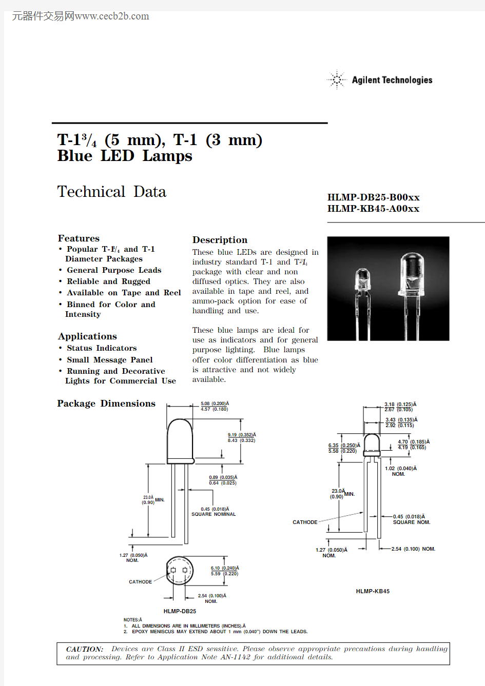
D: T-1 3/4 (5 mm)
K: T-1 (3 mm)
Absolute Maximum Ratings at T A = 25?C
Parameter Blue Units
Peak Forward Current70mA
DC Current[1]30mA
Reverse Voltage (I R = 100 μA)5V
Transient Forward Current[2]350mA
(10 μsec Pulse)
LED Junction Temperature115?C
Operating Temperature–20 to +80?C
Storage Temperature–30 to +100?C
Lead Soldering Temperature 260°C for 5 seconds
[1.6 mm (0.063 in.) from body]
Notes:
1.Derate linearly from 50 °C as shown in Figure 6.
2.The transient peak current is the maximum non-recurring peak current that can be
applied to the device without damaging the LED die and wirebond. It is not
recommended that this device be operated at peak currents above the Absolute
Maximum Peak Forward Current.
Optical Characteristics at T A = 25?C
Luminous Color,Viewing Intensity Dominant Peak Angle I V (mcd)Wavelength Wavelength 2θ1/2[2]@ I F = 20 mA
λd [1] (nm)λPEAK (nm)
Degrees Part Number Typ.
Typ.
Typ.HLMP-DB25-B00xx 40 10046242625HLMP-KB45-A00xx 30 45
462
426
40
Min. Typ.Notes:
1.The dominant wavelength, λd , is derived from the CIE chromaticity diagram and represents the single wavelength which defines the color of the device.
2. θ1/2 is the off-axis angle at which the luminous intensity is half of the axial luminous intensity.
Electrical Characteristics at T A = 25?C
Thermal Forward Reverse Resistance
Voltage Breakdown Speed Capacitance R θJ-PIN (°C/W)V F (Volts)V R (Volts)Response C (pF), V F = 0,Junction to Part
@ I F = 20 mA @ I R = 100 μA τs (ns) f = 1 MHz Cathode Lead Number Typ. Max. Min. Typ.Typ.Typ.Typ.
HLMP-DB25-B00xx 4.0 5.0 5.0 3050097260HLMP-KB45-A00xx
4.0
5.0
5.0 30
500
97
290
Figure 1. Relative Intensity vs.Wavelength.Figure 3. Relative Intensity vs. Peak Forward Current (300 μs pulse width, 10 ms period).
Figure 2. Forward Current vs.Forward Voltage.
60503020035
1040214I F – F O R W A R D C U R R E N T – m A
V F – FORWARD VOLTAGE – V 1.01.6
1.2
R E L A T I V E L U M I N O U S I N T E N S I T Y (N O R M A L I Z E D A T 2
0 m A )
I P – PEAK FORWARD CURRENT – mA
20
406080
1.4
305070WAVELENGTH – nm
R E L A T I V E I N T E N S I T Y
1.0
0.5
350550700
400600450500650
Soldering/Cleaning
Cleaning agents from the ketone family (acetone, methyl ethyl ketone, etc.) and from the
chlorinated hydrocarbon family (methylene chloride,
trichloroethylene, carbon tetrachloride, etc.) are not
recommended for cleaning LED parts. All of these various
solvents attack or dissolve the encapsulating epoxies used to form the package of plastic LED parts.
For information on soldering LEDs, please refer to Application Note 1027.
Figure 8. Relative Luminous Intensity vs. Angular Displacement for HLMP-KB45.
Figure 7. Relative Luminous Intensity vs. Angular Displacement for HLMP-DB25.
Figure 6. Maximum DC Forward Current vs. Ambient Temperature.Derating Based on T J Max. = 115 °C.
Figure 5. Relative Luminous Intensity vs. Forward Current.
Figure 4. Forward Current vs.Forward Voltage.R A T I O O F P E A K C U R R E N T T O T E M P E R A T U R E D E R A T E D D C C U R R E N T
PULSE WIDTH (SECONDS)
1.20.4R E L A T I V E L U M I N O U S I N T E N S I T Y (N O R M A L I Z E D A T 20 m A )
I F – DC FORWARD CURRENT – mA
0102035
0.851525300.30.20.10.50.60.70.91.01.1I F – F O R W A R D C U R R E N T – m A D C
0T A – AMBIENT TEMPERATURE – °C
3070352010105030805152520406090
Intensity Bin Limits
Intensity Range (mcd)
Bin Min.Max.
A30.040.0
B40.050.0
C50.065.0
D65.085.0
E85.0110.0
F110.0140.0
G140.0180.0
H180.0240.0
J240.0310.0
K310.0400.0
L400.0520.0
M520.0680.0
N680.0880.0
Color Bin Limits
(nm at 20 mA)
Blue nm @ 20 mA
Bin ID Min.Max.
1460.0464.0
2464.0468.0
3468.0472.0
4472.0476.0
5476.0480.0
Tolerance for each bin limit will be ±0.5nm.
Mechanical Option Matrix
Mechanical Option Code Definition
00Bulk Packaging, minimum increment 500 pcs/bag
02Tape & Reel, straight leads, minimum increment 1300 pcs/bag
DD Ammo Pack, straight leads with minimum increment
Note:
All categories are established for classification of products. Products may not be available in all categories. Please contact your local Agilent representative for further clarification/information.
https://www.doczj.com/doc/dc8731236.html,/semiconductors For product information and a complete list of distributors, please go to our web site.
For technical assistance call:
Americas/Canada: +1 (800) 235-0312 or (408) 654-8675
Europe: +49 (0) 6441 92460
China: 10800 650 0017
Hong Kong: (+65) 6756 2394
India, Australia, New Zealand: (+65) 6755 1939 Japan: (+81 3) 3335-8152 (Domestic/Interna-tional), or 0120-61-1280 (Domestic Only) Korea: (+65) 6755 1989
Singapore, Malaysia, Vietnam, Thailand, Philippines, Indonesia: (+65) 6755 2044 Taiwan: (+65) 6755 1843
Data subject to change.
Copyright ? 2003 Agilent Technologies, Inc. Obsoletes 5988-2226EN
May 12, 2003
5988-9507EN