Parameter
Max.
Units
V DS
Drain- Source Voltage
-30V I D @ T A = 25°C Continuous Drain Current, V GS @ -10V -3.0I D @ T A = 70°C Continuous Drain Current, V GS @ -10V -2.4A
I DM
Pulsed Drain Current -24P D @T A = 25°C Power Dissipation 1.25P D @T A = 70°C Power Dissipation 0.80Linear Derating Factor 10mW/°C V GS
Gate-to-Source Voltage
± 20V T J, T STG
Junction and Storage Temperature Range
-55 to + 150
°C
04/30/03
Parameter
Max.
Units
R θJA
Maximum Junction-to-Ambient
100
°C/W
Thermal Resistance
Absolute Maximum Ratings
W https://www.doczj.com/doc/fc3517085.html, 1
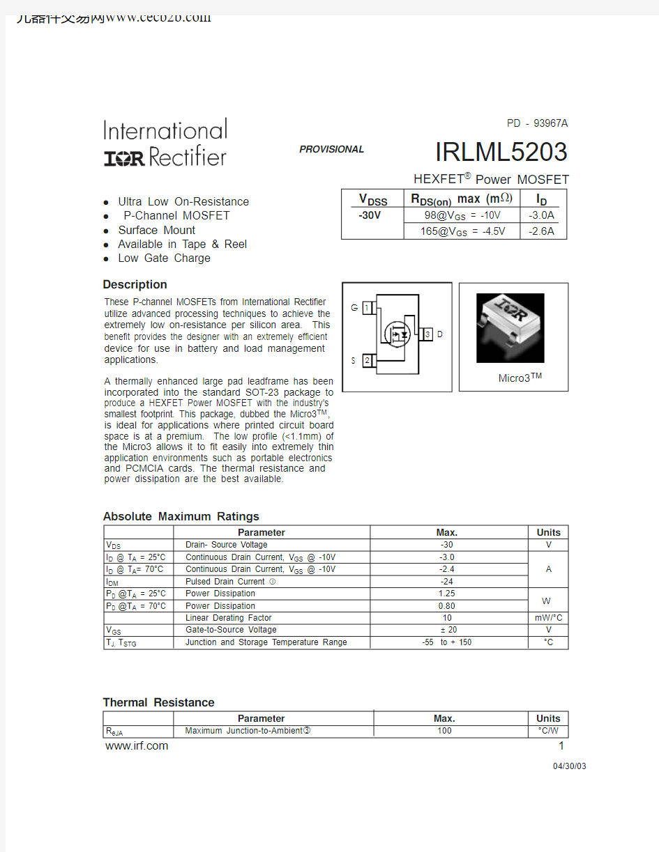
produce a HEXFET Power MOSFET with the industry's smallest footprint. This package, dubbed the Micro3TM ,is ideal for applications where printed circuit board space is at a premium. The low profile (<1.1mm) of the Micro3 allows it to fit easily into extremely thin application environments such as portable electronics and PCMCIA cards. The thermal resistance and power dissipation are the best available.
l Ultra Low On-Resistance l P-Channel MOSFET l Surface Mount
l Available in Tape & Reel
IRLML5203
https://www.doczj.com/doc/fc3517085.html,
PROVISIONAL
Source-Drain Ratings and Characteristics
Repetitive rating; pulse width limited by
max. junction temperature.
Notes:
Pulse width ≤ 400μs; duty cycle ≤ 2%.
Surface mounted on FR-4 board, t ≤ 5sec.
Parameter
Min.Typ.Max.Units Conditions V (BR)DSS
Drain-to-Source Breakdown Voltage -30––––––V V GS = 0V, I D = -250μA
?V (BR)DSS /?T J
Breakdown Voltage Temp. Coefficient –––0.019–––V/°C Reference to 25°C, I D = -1mA –––––– 98V GS = -10V, I D = -3.0A
–––––– 165V GS = -4.5V, I D = -2.6A V GS(th)
Gate Threshold Voltage -1.0–––-2.5V V DS = V GS , I D = -250μA g fs Forward Transconductance 3.1––––––S V DS = -10V, I D = -3.0A ––––––-1.0V DS = -24V, V GS = 0V
––––––-5.0V DS = -24V, V GS = 0V, T J = 70°C Gate-to-Source Forward Leakage ––––––-100V GS = -20V
Gate-to-Source Reverse Leakage ––––––100V GS = 20V Q g Total Gate Charge
–––9.514I D = -3.0A Q gs Gate-to-Source Charge
––– 2.3 3.5nC V DS = -24V Q gd Gate-to-Drain ("Miller") Charge ––– 1.6 2.4V GS = -10V t d(on)Turn-On Delay Time –––12–––V DD = -15V t r Rise Time
–––18–––I D = -1.0A
t d(off)Turn-Off Delay Time –––88–––R G = 6.0?t f Fall Time
–––52–––V GS = -10V C iss Input Capacitance –––510–––V GS = 0V C oss Output Capacitance
–––71–––pF V DS = -25V C rss
Reverse Transfer Capacitance
–––
43
–––? = 1.0MHz
Electrical Characteristics @ T J = 25°C (unless otherwise specified)
I GSS μA
m ?
R DS(on)Static Drain-to-Source On-Resistance I DSS Drain-to-Source Leakage Current nA
ns
IRLML5203
https://www.doczj.com/doc/fc3517085.html, 3
PROVISIONAL
Vs. Temperature
IRLML5203
https://www.doczj.com/doc/fc3517085.html,
PROVISIONAL
Fig 8. Maximum Safe Operating Area
Gate-to-Source Voltage
Fig 5. Typical Capacitance Vs.Drain-to-Source Voltage
Forward Voltage
IRLML5203
https://www.doczj.com/doc/fc3517085.html, 5
PROVISIONAL
Case Temperature
V DD
V V t t t t Fig 10a. Switching Time Test Circuit
Fig 10b. Switching Time Waveforms
IRLML5203
https://www.doczj.com/doc/fc3517085.html,
PROVISIONAL
Fig 12. Typical On-Resistance Vs. Drain
Current
Fig 11. Typical On-Resistance Vs. Gate
Voltage
Fig 13b. Gate Charge Test Circuit
Fig 13a.
Basic Gate Charge Waveform V
DS
Current Sampling Resistors
4
8
12
16
-I D , Drain Current (A)
0.00
0.10
0.20
0.30
0.40
R D S (o n ) , D r a i n -t o -S o r c e O n R e s i s t a n c e (?)
-V GS, Gate -to -Source Voltage (V)
R D S (o n ), D r a i n -t o -S o u r c e O n R e s i s t a n c e (?)
https://www.doczj.com/doc/fc3517085.html, 7
Fig 14. Threshold Voltage Vs. Temperature
Fig 15. Typical Power Vs. Time
0.001
0.0100.100 1.00010.000100.000
Time (sec)
T J , Temperature ( °C )
-V G S (t h ) , V a r i a c e ( V )
IRLML5203
https://www.doczj.com/doc/fc3517085.html,
PROVISIONAL
Dimensions are shown in millimeters (inches)
Micro3TM Package Outline
LEAD ASSIGNMENTS 1 - GATE 2 - SOURCE 3 - DRAIN
L 3X
3X
C θ
A1
- C -B 3X
A
e
e1
0.008 (.003)
3
1
2
E - A -
- B -D H
0.20 ( .008 ) M A M
DIM
INCHES MILLIMETERS
MIN MAX MIN MAX A .032 .044 0.82 1.11A1 .001 .004 0.02 0.10B .015 .021 0.38 0.54C .004 .006 0.10 0.15D .105 .120 2.67 3.05e .0750 BASIC 1.90 BASIC e1 .0375 BASIC 0.95 BASIC
E .047 .055 1.20 1.40H .083 .098 2.10 2.50L .005 .010 0.13 0.25
θ 0° 8° 0° 8°0.10 (.004) M C A S B S
MINIMUM RECOMMENDED FOOTPRINT
0.80 ( .031 ) 3X
2.00( .079 )
0.95 ( .037 )
2X
0.90( .035 ) 3X
3
3
3
NOTES:
1. DIMENSIONING & TOLERANCING PER ANSI Y14.5M-198
2.2. CONTROLLING DIMENSION : INCH.
DIMENSIONS DO NOT INCLUDE MOLD FLASH.
IRLML5203
https://www.doczj.com/doc/fc3517085.html,
PROVISIONAL
Micro3TM Tape & Reel Information
Dimensions are shown in millimeters (inches)
2.05 ( .080 )1.95 ( .077 )
TR
FEED DIRECTION
4.1 ( .161 )3.9 ( .154 )
1.6 ( .062 )1.5 ( .060 )
1.85 ( .072 )1.65 ( .065 )
3.55 ( .139 )3.45 ( .136 )
1.1 ( .043 )0.9 ( .036 )4.1 ( .161 )3.9 ( .154 )
0.35 ( .013 )0.25 ( .010 )
8.3 ( .326 )7.9 ( .312 )
1.32 ( .051 )1.12 ( .045 )
9.90 ( .390 )8.40 ( .331 )
178.00( 7.008 ) MAX.
NOTES:
1. CONTROLLING DIMENSION : MILLIMETER.
2. OUTLINE CONFORMS TO EIA-481 & EIA-541.
Data and specifications subject to change without notice.
IR WORLD HEADQUARTERS: 233 Kansas St., El Segundo, California 90245, USA Tel: (310) 252-7105
TAC Fax: (310) 252-7903
Visit us at https://www.doczj.com/doc/fc3517085.html, for sales contact information . 04/03