Three-stage multiphase-switched-capacitor boost DC-AC inverter
Yuen-Haw Chang ?,?and Zih-Yao Luo ?,m
Department and Graduate Institute of Computer Science and Information Engineering ,
Chaoyang University of Technology ,Taichung ,Taiwan
SUMMARY
A closed-loop scheme of a three-stage multiphase-switched-capacitor boost DC-AC inverter (MPSCI)is proposed by combining the multiphase operation and sinusoidal-pulse-width-modulation (SPWM)control for low-power step-up DC-AC conversion and regulation.In this MPSCI,the power unit contains two parts:MPSC booster (front)and H-bridge (rear).The MPSC booster is suggested for an inductor-less step-up DC-DC conversion,where three voltage doublers in series are controlled with multiphase operation for boosting voltage gain up to 23=8at most.The H-bridge is employed for DC-AC inversion,where four solid-state switches in H-connection are controlled with SPWM to obtain a sinusoidal AC output.In addition,SPWM is adopted for enhancing output regulation not only to compensate the dynamic error,but also to reinforce robustness to source /loading variation.The relevant theoretical analysis and design include:MPSCI model,steady-state /dynamic analysis,voltage conversion ratio,power ef?ciency,stability,capacitance selection,total harmonic distortion (THD),output ?lter,and closed-loop control design.Finally,the closed-loop MPSCI is simulated,and the hardware circuit is implemented and tested.All the results are illustrated to show the ef?cacy of the proposed scheme.Copyright ?2011John Wiley &Sons,Ltd.
Received 27November 2009;Revised 5January 2011;Accepted 7January 2011
KEY WORDS :multiphase-switched-capacitor (MPSC);boost DC-AC inverter;multiphase operation;sinusoidal-pulse-width-modulation (SPWM).
1.INTRODUCTION
In the application of portable electronic equipments,power modules are always asked for some features,such as small volume,lightweight,high power density /power ef?ciency,and good output regulation.The switched-capacitor (SC)power converter,possessed of the power stage based on charge pump structure,is one of the good solutions to low-power DC-DC conversion because it has only semiconductor switches and capacitors.Unlike traditional ones,SC converter needs no magnetic element,e.g.inductor and transformer,so such an inductor-less converter always has lightweight,small volume,and low EMI.
A charge pump SC converter is usually designed to obtain an output higher than supply voltage or a reverse-polarity voltage.Such a step-up /reverse function is suitable to many applications,e.g.power-transistor,op-amp,?ash EEPROM,white LED,?uorescent lamp,and LCD drivers [1].In fact,the SC idea has existed over half a century.In 1932,Cockroft and Walton implemented a capacitor-diode voltage multiplier in the particle accelerator of the nuclear reaction.In 1971,Brugler ?Correspondence to:Yuen-Haw Chang,Department and Graduate Institute of Computer Science and Information Engineering,Chaoyang University of Technology,Taichung,Taiwan.?E-mail:cyhfyc@https://www.doczj.com/doc/fe10049911.html,.tw ?Correspondence to:Zih-Yao Luo,Department and Graduate Institute of Computer Science and Information Engineering,Chaoyang University of Technology,Taichung,Taiwan.§E-mail:kibdnet@https://www.doczj.com/doc/fe10049911.html,
INTERNATIONAL JOURNAL OF CIRCUIT THEORY AND APPLICATIONS Int.J.Circ.Theor.Appl.Published online (.com).DOI:10.1002/cta.2012;:–40wileyonlinelibrary in Wiley Online Library 120178779025February 161
878
Y.-H.CHANG AND Z.-Y.LUO
suggested SC voltage multiplier[2],and then Lin and Chua presented the relevant topological analysis[3].Recently,many applications are expanding as:transformerless large-conversion-ratio converter[4],bidirectional SC converter[5],and pseudo-continuous SC voltage doubler[6].Up to now,the various SC types have been suggested for power conversion,and some well-known topologies are(i)Dickson charge pump,(ii)Ioinovici SC converter,(iii)Ueno charge pump,and (iv)Makowski charge pump.In1976,Dickson charge pump was proposed based on a diode-chain structure with two-phase operation via pumping capacitors[7].It provides voltage gain proportional to the stage number of pumping capacitors,and its dynamic model and ef?ciency analysis were discussed[8,9].But,its drawbacks include the?xed voltage gain and larger device area.In 1993,Ioinovici et al.suggested a voltage-mode SC converter with two symmetrical capacitor cells working complementarily,and used PWM for the?exible voltage gain[10,11].In1994, Ngo et al.?rst proposed a current control of SC converters by using a saturated transistor as a controllable current source[12].In1997,Zhu et al.performed a comprehensive and accurate steady-state analysis of step-up SC converter[13].In1998,Mak et al.proposed an SC inverter with high power density and enhanced regulation capability[14].Following this,Chang proposed an integrated scheme of SC step-up/down DC-DC/DC-AC converter[15,16].Recently,Axelrod et al.suggested a hybrid SC/inductor converter[17],and Tan et al.proposed a low-EMI SC by interleaving control[18].However,Ioinovici SC provides voltage gain proportional to the number of pumping capacitors.
In1991,Ueno proposed lots of the new known structures:series–parallel,Fibonacci,etc.The four-stage SC transformer idea was proposed for step-up ratio of Fibonacci series to realize an emergency power supply[19],and a low ripple-noise SC converter was presented[20].However,their converters sufferedfrom alimitedlineregulationcapability.In1997,Makowskisuggestedacanonicalstructureof multiplier charge pump with two-phase cascaded voltage doublers[21].An n-stage Makowski charge pump can obtain voltage gain limited by the(n+1)th Fibonacci number.Its relevant steady-state analysis,voltage/power loss were discussed,and it had been proved just to require the least number of pumping capacitors in two-phase SC[22,23].In2001,Starzyk proposed a new scheme of multiphase voltage doubler by using multiphase operation different from previous two-phase operation[24]. Further,the relevant performance limits were discussed,and the relationship(voltage gain and phase number)was presented by generalized Fibonacci number[25,26].An n-stage Starzyk charge pump can boost voltage gain up to2n at most,i.e.the number of pumping capacitors in Starzyk is required fewer than that in Makowski for the same voltage gain.Nevertheless,some improved spaces still exist, and the SC development for DC-AC is still not enough.Here,our paper targets some points as follows.
(i)By using multiphase operation from Starzyk’s idea,the multiphase-switched-capacitor(MPSC) booster is presented as the inductor-less front stage of the inverter to obtain the higher voltage gain with the less(or least)number of pumping capacitors.Most importantly,the realization of timing-control circuit for multiphase operation must be simple.(ii)Since the source voltage is decreasing with the running time of batteries,or varying due to bad-quality ones,perhaps lots of source noises occur.In addition,the loading variation often results from the unexpected load failure or adding/removing the load.But,Starzyk circuit is?xed,so output regulation/robustness capability is limited.Here,by using sinusoidal-pulse-width-modulation(SPWM)control,the closed-loop MPSC-based DC-AC inverter is realized to enhance output regulation for different desired outputs,as well as robustness against source/loading variation.
2.CONFIGURATION OF MPSCI
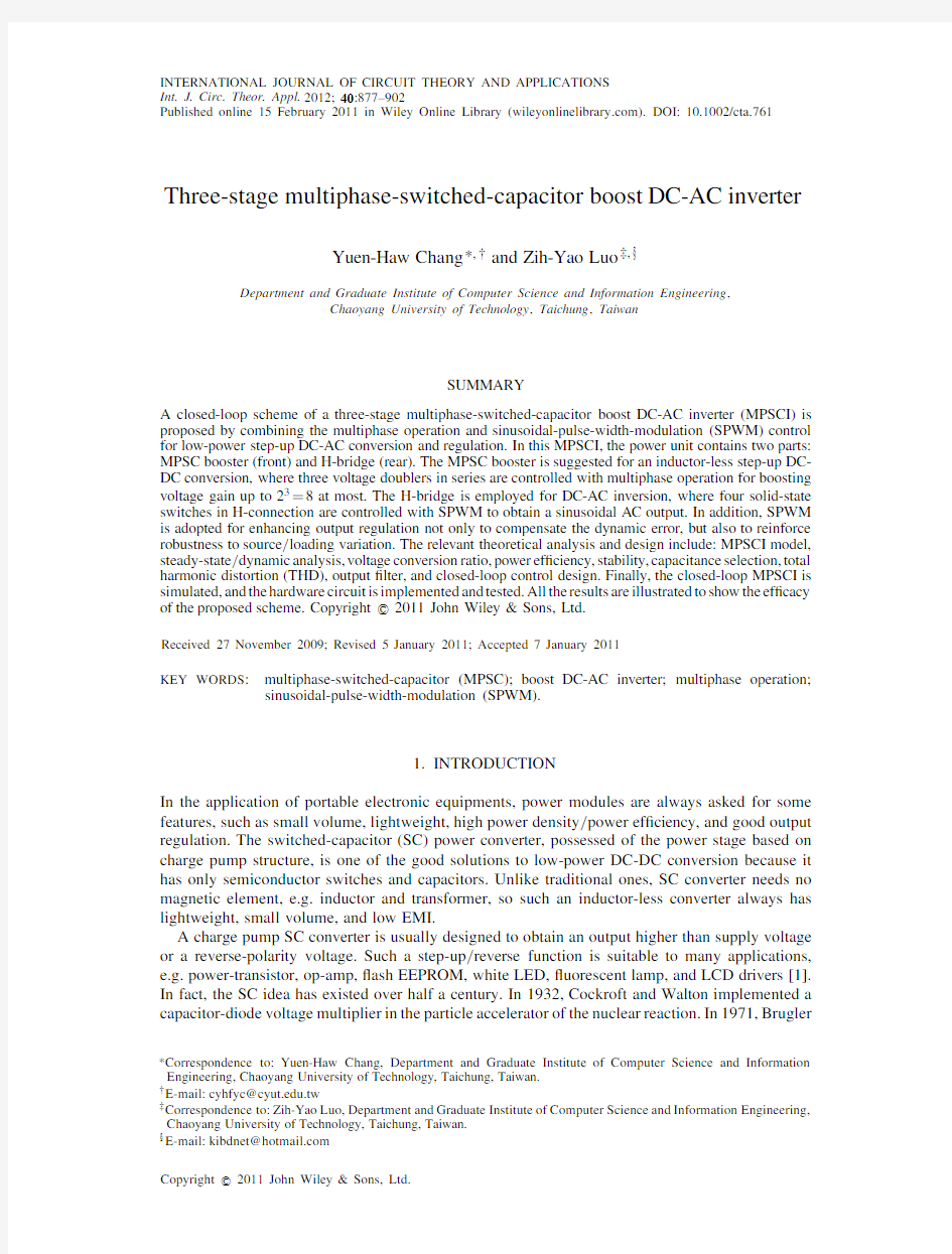
Figure1shows the closed-loop MPSCI.It contains two major units:‘power unit’and‘control unit’as shown in the upper and lower half of Figure1.The power unit:MPSC-based inverter is composed of MPSC booster(front)and H-bridge(rear),connected in series for step-up DC-AC conversion.The control unit:the SPWM controller is mainly composed of SWPM block and phase generator,working in charge of duty-cycle control and timing control of multiphase operation. First,let us consider the MPSC booster.As shown in Figure1,the three-stage MPSC booster is presented based on Starzyk charge pump[24],and composed of three cascaded voltage doublers
THREE-STAGE MPSC BOOST DC-AC
INVERTER Figure 1.Con?guration of MPSC-based boost DC-AC inverter.
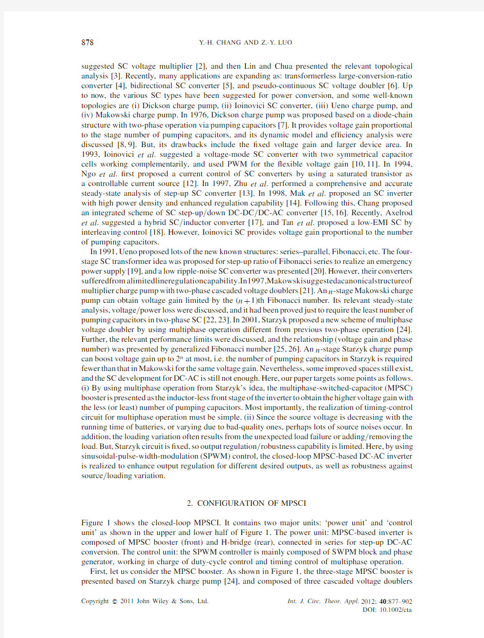
in series connection between source V S and buffer capacitor voltage v C b .Its main function is to boost v C b up to 23=8times the voltage of V S at most.For more details,it includes three pumping capacitors C 1,C 2,C 3,buffer capacitor C b ,and 12MOSFET switches S 1,S 2,S 3,...,S 12,where each capacitor has the same capacitance C (C 1=C 2=C 3=C )with equivalent series resistance (ESR)r C ,the buffer capacitor has the larger capacitance C b ,and S 1,S 2,S 3,...,S 12are operated as switches with the on-state resistance r T .Figure 2shows the theoretical waveforms of multiphase operation in the MPSC booster,where T S is the MPSC cycle (T S =1/f S ,f S :MPSC frequency).Here,assume that one T S contains eight phases (Phase I,II,III,...,VIII,phase number is p =8),and each phase has the same phase cycle T (T =T S /8).Let us discuss Phase I–VIII operations.(i)Phase I:turn on S 1,S 2.Then,the Phase I topology is shown in Figure 3(a):capacitor voltage v C 1across C 1is charged up to V S and C b is discharged to supply load R L in the H-bridge.(ii)Phase II:turn on S 3,S 4,S 5,S 6.The Phase II topology is in Figure 3(b):v C 2across C 2is charged by V S ,v C 1in series and C b is discharged to supply R L .(iii)Phase III:it repeats the Phase I operation.(iv)Phase IV:turn on S 3,S 4,S 7,S 8,S 9,S 10.The Phase IV topology is in Figure 3(c):v C 3across C 3is charged by V S ,v C 1,v C 2in series,and C b is still discharged to supply R L .(v)–(vii)Phase V–VII:the operations in Phase V /VI /VII are identical to those in Phase I /II /III,respectively.(viii)Phase VIII:turn on S 3,S 4,S 7,S 8,S 11,S 12.The Phase VIII topology is shown in Figure 3(d):C b is charged under the series connection of V S ,v C 1,v C 2,v C 3,and simultaneously discharged to supply R L .Since v C 1/v C 2/v C 3is charged toward the goal value of V S /2V S /4V S ,v C b can be boosted up to 8times the voltage of V S at most.Thus,this MPSC booster is capable of supplying 8V S to H-bridge at most.Next,let us look at H-bridge.As shown in Figure 1,the structure of H-bridge is a full-wave bridge connection between v C b and v o ,and the main function 879
Y .-H.CHANG AND Z.-Y .
LUO
Figure 2.Theoretical waveforms of multiphase operation in MPSC booster.
is to convert v C b (DC)into alternating output v o (AC).For more details,it includes four MOSFETs S +A ,S ?A ,S +B ,S ?B connected with four diodes in parallel (assume that all the on-state resistances are r T as above).With the help of SPWM controller,the driver signals of S +A ,S ?A ,S +B ,S ?B are generated to keep v o on following the desired sinusoidal reference V ref .In addition,there is a power-usage band-stop ?lter (BSF)connected with the output terminal in parallel,including ?lter inductor L F and capacitor C F .The main function is to obtain a harmonic trap so as to eliminate some harmonics of v o for the better THD.
Second,the control unit:the SPWM controller is shown in the lower half of Figure 1which is composed of low-pass ?lter (LPF),SPWM block and phase generator.First,the phase generator is designed with digital programmable chip /frequency divider (FD)as a timing-control circuit for multiphase operation,and it is required to generate the driver signals S 1?S 12as shown the waveforms in Figure 2.At the same time,from the view of signal ?ow,v o is fedback into LPF for high-frequency noise rejection.And then,the ?ltered V o is compared with V ref in the SPWM block so as to obtain the tracking error signal e ,as well as the control signal v con via a gain compensator.Next,by comparing v con with V ramp (saw-toothed ramp),the driver signal S +A is obtained in A-arm,and its duty cycle is denoted by D A (0 D A 1).By inverting S +A ,the driver signal S ?A is obtained and its duty cycle is 1?D A .Similarly,by comparing ?v con (opposite of v con )with V ramp ,D B /1?D B can be obtained as the duty cycle of S +B
/S ?B in the B-arm (0 D B 1).880
THREE-STAGE MPSC BOOST DC-AC
INVERTER Figure 3.Topologies of three-stage MPSC booster:(a)Phase I,III,V ,VII;(b)Phase II,VI;(c)Phase IV;and (d)Phase VIII.
Figure 4shows the theoretical waveforms of SPWM in H-bridge.Obviously,because the A-arm and B-arm are controlled via a set of complementary control signals (v con ,?v con ),the relationship (D A ,D B )is easily obtained as:D A +D B =1.When S +A ,S ?B (S ?A ,S +B )turn on simultaneously,the effective positive (negative)output of v o is expectable.For the good of explanation,we take AND-logic combination of S +A ,S ?B to obtain S +?AB as in Figure 4,where D +?AB is the duty cycle of S +?AB to handle the effective positive output,and D +?AB (0 D +?AB 1)can be presented as:(i)D +?AB =2D A ?1,0.5 D A 1;(ii)D +?AB =0,0 D A 0.5.Similarly,S ?+AB is obtained by AND-logic of S ?A ,S +B as in Figure 4,and its duty cycle D ?+AB is in charge of the effective negative output with the relationship as:(i)D ?+AB =2D B ?1,0.5 D B 1;(ii)D ?+AB =0,0 D B 0.5.Let us summarize the above descriptions together in Figure 5.In this ?gure,the upper 2sub-graphs show the relationships about D +?AB ?D A and D ?+AB ?D B ,where D A ,D B are the practical signals produced by the SPWM block,and D +?AB ,D ?+AB are the analytic variables for the convenience of theoretical analysis and design.Thus,the positive (negative)half-cycle output of v o is regulated relative to how long D +?AB ·T PWM (D ?+AB ·T PWM )is,where T PWM is the SPWM cycle (T PWM =1/f PWM ,f PWM :SPWM frequency).In general,the MPSC frequency f S is suggested to be taken at 10times or higher value of f PWM for step-up performance of MPSC booster.
881
Y .-H.CHANG AND Z.-Y .
LUO
Figure 4.Theoretical waveforms of SPWM in
H-bridge.
Figure 5.Duty cycle relationship.
882
THREE-STAGE MPSC BOOST DC-AC INVERTER
An additional remark is given here about phase number.The suf?cient phase number is p=4for the maximum voltage gain being8[25].In our paper,the phase number is taken by p=8,and it seems to be a little redundant in time execution.We have some reasons to keep the redundancy as follows.(i)The timing-control circuit(phase generator)is made easier.As shown in Figure2,we need three sets of symmetrical driver signals as:[S1,S2and S3,S4],[S5,S6and S7,S8],[S9,S10 and S11,S12]for multiphase operation.It is noticeable that these waveforms are symmetrical.In one T S(360?),[S1,S2]is leading45?ahead of[S3,S4],[S5,S6]is leading90?ahead of[S7,S8],
and[S9,S10]is leading180?ahead of[S11,S12].Hence,such a symmetrical regularity makes the realization of phase generator much easier.(ii)When the phase number is p=4(T S has four phases),v C1across C1is charged once(Phase I)per four phases.In our paper,the phase number is p=8(T S has eight phases),v C1across C1is charged four times(Phase I,III,V,VII)per eight phases.According to charge distribution,charging four times per eight phases is more helpful to
boosting response,even though the switching cycle of p=8is1
2cycle longer than that of p=4.
Of course,we need a larger buffer capacitor C b for p=8,but not very large.If p=4,C b has to
stand up alone for3
4cycle to supply the load.In our paper(p=8),C b has to supply the load
alone for7
8cycle.By comparing the two cases,our buffer capacitor C b is needed just7
6
times the
capacitance value of C b of p=4.
3.FORMULATION OF MPSCI
In the beginning,we start with the Thevenin equivalent model of the MPSC booster.And then, based on this equivalent model,the overall description of MPSC-based DC-AC inverter is derived, and it will be helpful to the theoretical analysis and control design later.
3.1.Formulation of MPSC booster
Let us discuss the Thevenin equivalent model of the MPSC booster.First,we remove H-bridge from the power unit,and set the circuit open temporarily.Within one T S,there are eight phase operations to be considered as follows.In Phase I,let S1,S2be on,and the topology is in Figure3(a). According to this topology,the dynamic equation for Phase I can be described as
???
????v C
1
(t)
v C
2
(t)
v C
3
(t)
v C
b
(t)
?
??
??
??=
?
??
??
??
?
?1
R p C
000
0000
0000
0000
?
??
??
??
?
·
?
??
??
?
v C
1
(t)
v C
2
(t)
v C
3
(t)
v C
b
(t)
?
??
??
?
+
?
??
??
??
?
1
R p C
?
??
??
??
?
·V S,[Phase I,III,V,VII](1)
where R p=2·r T+r C is the parasitic resistance of three-stage MPSC booster.In Phase II,let S3,S4,S5,S6be on,and the topology is in Figure3(b).The dynamic equation for Phase II is described as:
???
????v C
1
(t)
v C
2
(t)
v C
3
(t)
v C
b
(t)
?
??
??
??=
?
??
??
??
??
?
?1
2R p C
1
2R p C
00
1
2R p C
?1
2R p C
00
0000
0000
?
??
??
??
??
?
·
?
??
??
?
v C
1
(t)
v C
2
(t)
v C
3
(t)
v C
b
(t)
?
??
??
?
+
?
??
??
??
??
?
?1
2R p C
1
2R p C
?
??
??
??
??
?
·V S.[Phase II,VI](2)
In Phase III,it repeats the Phase I operation.Hence,the dynamic equation for Phase III is identical to(1).In Phase IV let S3,S4,S7,S8,S9,S10be on,and the topology is in Figure3(c).The dynamic
883
Y.-H.CHANG AND Z.-Y.LUO equation for Phase IV is derived as:
???
????v C
1
(t)
v C
2
(t)
v C
3
(t)
v C
b
(t)
?
??
??
??=
?
??
??
??
??
??
??
?1
3R p C
?1
3R p C
1
3R p C
?1
3R p C
?1
3R p C
1
3R p C
1
3R p C
1
3R p C
?1
3R p C
0000
?
??
??
??
??
??
??
·
?
??
??
?
v C
1
(t)
v C
2
(t)
v C
3
(t)
v C
b
(t)
?
??
??
?
+
?
??
??
??
??
??
??
?1
3R p C
?1
3R p C
1
3R p C
?
??
??
??
??
??
??
·V S.[Phase IV](3)
Next,the operations in Phase V/VI/VII are identical to those in Phase I/II/III,hence the dynamic equations for Phase V/VI/VII are completely identical to(1)/(2)/(1).Finally,in Phase VIII let S3,S4,S7,S8,S11,S12be on.The Phase VIII topology is in Figure3(d).Hence,the dynamic equation for Phase VIII is derived as:
???
????v C
1
(t)
v C
2
(t)
v C
3
(t)
v C
b
(t)
?
??
??
??=
?
??
??
??
??
??
??
?
?
?1
3R p C
?1
3R p C
?1
3R p C
1
3R p C
?1
3R p C
?1
3R p C
?1
3R p C
1
3R p C
?1
3R p C
?1
3R p C
?1
3R p C
1
3R p C
1
3R p C b
1
3R p C b
1
3R p C b
?1
3R p C b
?
??
??
??
??
??
??
?
?
·
?
??
??
?
v C
1
(t)
v C
2
(t)
v C
3
(t)
v C
b
(t)
?
??
??
?
+
?
??
??
??
??
??
??
?
?
?1
3R p C
?1
3R p C
?1
3R p C
1
3R p C b
?
??
??
??
??
??
??
?
?
·V S.[Phase VIII]
(4)
Based on(1)–(4),the open-circuit dynamic equation of the MPSC booster can be derived by state–space average technique[11,14],[(1)+(2)+(1)+(3)+(1)+(2)+(1)+(4)]/8,to be formulated as x 8x(t)=A8x·x8x(t)+B8x·V S,v C b(t)=C8x·x8x(t),(5a,b) where
x8x(t)=[v C
1(t)v C
2
(t)v C
3
(t)v C
b
(t)]T,(6a)
A8x=?
??
??
??
??
??
??
??
?17
24R p C
1
24R p C
1
24R p C
1
24R p C
?5
24R p C
1
24R p C
00
?2
24R p C
1
24R p C
1
24R p C b
1
24R p C b
1
24R p C b
?1
24R p C b
?
??
??
??
??
??
??
??
,B8x=
?
??
??
??
??
??
??
7
24R p C
1
24R p C
1
24R p C b
?
??
??
??
??
??
??
,C8x=[0001].
(6b,c,d)
According to(5),the?rst-order equivalent model of the MPSC booster will be derived.In the ?rst-order model,there are two parameters to be determined as:boosting gain and dominant pole. First,let us look at boosting gain.For DC analysis,by substituting x 8x=0of(5),the steady-state buffer capacitor voltage V C
b
can be
V C
b =(?C8x A?18x B8x)·V S=8·V S.(7)
884
THREE-STAGE MPSC BOOST DC-AC INVERTER
Obviously,V C
b can be boosted up to8times voltage of V S,i.e.the boosting gain is8.In fact,
this is an open-circuit result.When the load is added in,the boosting gain will be lower than 8.Second,the dominant pole of MPSC booster is discussed here.Based on(6b),A8x is divided into four sub-matrixes A11~A22,and then A8x can be decomposed as(8a),where the diagonal sub-matrix 8x is presented as shown in(8b):
A8x=?
??
??
??
??
??
??
??
?
?17
24R p C
1
24R p C
1
24R p C
1
24R p C
?5
24R p C
1
24R p C
00
?2
24R p C
1
24R p C
1
24R p C b
1
24R p C b
1
24R p C b
?1
24R p C b
?
??
??
??
??
??
??
??
?
=
A11A12
A21A22
=
I0
A21·A?111I
×
A110
0 8x
·
I A?1
11
·A12
0I
,(8a) 8x=A22?A21·A?111·A12=
?1
24R p C b
?
1
24R p C b
1
24R p C b
1
24R p C b
×
?
??
??
??
??
?
?17
24R p C
1
24R p C
1
24R p C
?5
24R p C
00
?2
24R p C
?
??
??
??
??
?
?1?
??
??
??
??
?
1
24R p C
1
24R p C
1
24R p C
?
??
??
??
??
?
=
?1
m·R p C b
.(8b)
Here,the value of m is computed at about112(m=112)when C b 100·C.Since the main goal of the MPSC booster is to realize step-up DC-DC conversion and supply,C b must be chosen larger for the better DC quality.Here,we assume that C b is taken by100times(or larger)value of C. Based on this assumption,it is obvious that the value of R p C b in 8x is much larger than R p C in A11(R p C b R p C).Hence, 8x of(8b)is the dominant pole of the MPSC booster.By combining (7)and(8b),the?rst-order approximated model of MPSC booster can be
v C
b =8·V S
m·R p C b·s+1
.(9)
Based on(9),the Thevenin equivalent model of the MPSC booster can be presented as shown in
Figure6.The equivalent circuit will be useful to the formulation of
MPSCI.
Figure6.Thevenin equivalent circuit of MPSC booster.
885
Y .-H.CHANG AND Z.-Y .LUO
3.2.Formulation of MPSC-based inverter
As shown in Figure 4,the A-arm /B-arm of H-bridge are practically controlled by D A /D B obtained by comparing v con /?v con and V ramp .As the above descriptions,the effective positive /negative output of v o can be regulated by D +?AB /D ?+AB ,and the relationships (D +?AB ?D A ,D ?+AB ?D B )are shown in upper 2sub-graphs of Figure 5.According to Figures 4and 5,it is concluded that H-bridge contains four different modes (Mode I,II,III,IV)listed as follows:
(i)
Mode I (v con >0):D +?AB =2D A ?1,for 0.5 D A 1;(ii)
Mode II (v con >0):D +?AB =0,for 0 D A 0.5;(iii)
Mode III (v con <0):D ?+AB =2D B ?1,for 0.5 D B 1;(iv)Mode IV (v con <0):D ?+AB =0,for 0 D B 0.5.
Next,according to the four modes,the formulation of MPSCI is derived as follows.In Mode I (v con >0):S +A ,S ?B are on for the period of D +?AB ·T PWM .By combining the equivalent circuit of the MPSC booster,the topology is obtained as in Figure 7(a).According to this topology,the dynamic equation for Mode I can be described as
????v C F (t )i L F (t )v C b (t )????=?????????01
C F
0?1L F ?(2r T R L )
L F
R L L F ·(R L +2r T )0?R L
C b ·(R L +2r T )?1C b 1m R p +1R L +2r T ?????????·???v C F (t )i L F (t )v C b (t )???+??????008m R p C b
??????·V S ,(10a)
v o (t )i S (t ) =????0?(2r T R L )R L R L +2r T 00?1m R p ????·???v C F (t )i L F (t )v C b (t )???+???08m R p ???·V S [Mode I](10b)
where i L F /v C F represents the ?lter inductor current /capacitor voltage of BSF,and i S is the supply-terminal current.In Mode II (v con >0):S +A ,S +B or S ?A ,S ?B are on for the period of (1?D +?AB )·T PWM .In addition,the topology is obtained as shown in Figure 7(b),and then the dynamic equation for Mode II can be
????v C F (t )i L F (t )v C b (t )????=?
????????01C F 0?1L F ?(2r T R L )L F 00
0?1m R p C b ?????????·???v C F (t )i L F (t )v C b (t )???+??????008m R p C b ??????·V S ,(11a) v o (t )
i S (t ) =???0?(2r T R L )
000?1m R p
???·???v C F (t )i L F (t )v C b (t )???+???08m R p ???·V S [Mode II]
(11b)Based on Equation (10)–(11),the dynamic equation of MPSCI for v con >0can be derived by state–space average technique,i.e.((10)·D +?AB ·T PWM +(11)·(1?D +?AB )·T PWM )/T PWM ,to be formulated 886
THREE-STAGE MPSC BOOST DC-AC
INVERTER Figure 7.SPWM-based H-bridge topologies:(a)Mode I topology of MPSCI;(b)Mode II topology of MPSCI;(c)Mode III topology of MPSCI;and (d)Mode IV topology of MPSCI.
as:
????v C F (t )i L F (t )v C b (t )????=??????????01C F 0?1L F ?(2r T R L )L F D +?AB L F ·R L R L +2r T 0?D +?AB C b ·R L R L +2r T ?1C b 1m R p +D +?AB R L +2r T ?
?????????·???v C F (t )i L F (t )v C b (t )???+??????008m R p C b
??????·V S ,(12a)887
Y.-H.CHANG AND Z.-Y.LUO
v o(t) i S(t)
=
?
??
??
0?(2r T R L)
D+?
AB
·R L
R L+2r T
00
?1
m R p
?
??
??·
?
??
v C
F
(t)
i L
F
(t)
v C
b
(t)
?
??+
?
??
8
m R p
?
??·V
S for v con>0.(12b)
Similarly,Figure7(c)/(d)deals with the Mode III/IV topology for the period of D?+
AB ·T PWM/(1?
D?+ AB )·T PWM.According to the topologies,their dynamic equations for Mode III and IV can be
formed.And then,by using the average technique,the dynamic equation of MPSCI for v con<0is derived as:
???
?v C
F
(t)
i L
F
(t)
v C
b
(t)
?
??
?=
?
??
??
??
??
?
1
C F
?1
L F
?(2r T R L)
L F
?D
?+
AB
L F
·R L
R L+2r T
D?+
AB
C b
·R L
R L+2r T
?1
C b
1
m R p
+D
?+
AB
R L+2r T
?
??
??
??
??
?
·
?
??
v C
F
(t)
i L
F
(t)
v C
b
(t)
?
??+
?
??
??
?
8
m R p C b
?
??
??
?
·V S,
(13a)
v o(t)
i S(t)
=
?
??
??
0?(2r T R L)?
D?+
AB
·R L
R L+2r T
00
?1
m R p
?
??
??·
?
??
v C
F
(t)
i L
F
(t)
v C
b
(t)
?
??+
?
??
8
m R p
?
??·V
S for v con<0.(13b)
Here,for convenience to explain full-wave control,we take a new variable of integrated duty
cycle D with the de?nition as follows:(i)positive half-cycle:D=D+?
AB for v con>0(ii)negative
half-cycle:D=?D?+
AB for v con<0.Based on this de?nition,the waveform of S AB can be obtained
as in the bottom of Figure4,and its duty cycle is just D with the range of?1 D 1.Figure5
shows the whole relationships among D+?
AB ,D?+
AB
,and D.When0 D 1,it means that the
positive half-cycle of v o is running.When?1 D 0,the negative half-cycle of v o is working. Thus,the full-wave output of v o can be controlled by this integrated duty cycle D(?1 D 1). Finally,based on(12)–(13),in terms of the new D,the state–space description of MPSCI can be derived as
x (t)=A inv·x(t)+B inv·u(t),(14a)
y(t)=C inv·x(t),(14b) where
x(t)=[v C
F (t)i L
F
(t)v C
b
(t)]T,u(t)=[V S],y(t)=[v o(t)i S(t)]T,(15a,b,c)
A inv=?
??
??
??
??
1
C F
?1
L F
?(2r T R L)
L F
D
L F
·R L
R L+2r T
0?
D
C b
·R L
R L+2r T
?1
C b
1
m R p
+
|D|
R L+2r T
?
??
??
??
??
,B inv=
?
??
??
?
8
m R p C b
?
??
??
?
,
C inv=?
??
?
0?(2r T R L)
D·R L
R L+2r T
00
?1
m R p
?
??
?.(15d,e,f)
888
THREE-STAGE MPSC BOOST DC-AC INVERTER
4.ANALYSIS AND DESIGN OF MPSCI
4.1.Steady-state and dynamic analysis
For steady-state and dynamic analysis,all variables of(14a)are considered with static and
dynamic signals as:v C
F (t)=V C
F
+?v C
F
(t),i L
F
(t)=I L
F
+?i L
F
(t),v C
b
(t)=V C
b
+?v C
b
(t),D(t)=D+
?d(t),v
o(t)=V o+?v o(t),i S(t)=I S+?i
S(t),where V C F,I L F,V C b,D,V o,I S are the static operating
signals,and?v C
F (t),?i L F(t),?v C b(t),?d(t),?v o(t),?i S(t)represent the dynamic small-signal signals.First,
let us look at the steady-state analysis.By substituting x =0of(14a),the steady-state output voltage V o,output current I o,and supply-terminal current I S can be
V o=?C inv,1·A?1inv·B inv·u=
R L·D·8V S
R L+2r T+|D|·m R p
,I o=V o
R L
=D·8V S
R L+2r T+|D|·m R p
(16a,b)
I S=?C inv,2·A?1inv·B inv·u=
|D|·8V S
R L+2r T+|D|·m R p
=
|D|·I o
D
=|I o|,(16c)
where sub-matrix C inv,1/C inv,2is the?rst/second row of C inv.From(16a,b),it is obvious that V o is a function of D(?1 D 1).In other words,the value of V o is regulated by D,and even the polarity of V o can also be changed because of?1 D 1.In addition,as shown in(16c),I S equals the absolute value of I o(I S=|I o|).This is a reasonable result because I S has no negative current at supply terminal.
Next,let us consider dynamic analysis of MPSCI.Based on(14),by using small-signal analysis (around one static duty cycle D),the dynamic transfer function between?v o(t)and?d(t)can be derived as:
G(s)=?v o(s)
?d(s)
=
s2+
1
L F C F
s2+
2r T R L
L F
s+
1
L F C F
G1(s)
·
8V S
m R p C b
·R L
R L+2r T
s+
1
C b
1
m R p
+
|D|
R L+2r T
G2(s)
.(17)
Here,G(s)is formed by the product of G1(s)and G2(s).The?rst term:G1(s)results from the power-usage output?lter,which is a second-order BSF including L F and C F.This BSF is just like a harmonic trap to eliminate some harmonics of v o.The second term:G2(s)comes from MPSC booster plus loading effect,and its maximum output is really close to8V S when R L r T.The small-signal model of(17)will be helpful to control design later.
4.2.Conversion ratio and power ef?ciency
According to(16a),the voltage conversion ratio M inv can be suggested as:
M inv=V o
V S
=8·D
1+
2r T+|D|·m R p
R L
.(18)
If D=0,then M inv=0.If D=+1(D=?1),then the maximum(minimum)of M inv will be close to+8(?8)when R L r T,r C.In other words,V o can be converted into the voltage range of ?8V S~+8V S.For nominal conditions,the maximum attainable output V o is8V S-voltage drops in the charging and discharging circuits.Hence,R L is asked much larger than the parasitic r T,r C for the better conversion ratio.In fact,R L is about in -level,and r T,r C is about in m -level.
889
Y .-H.CHANG AND Z.-Y .LUO
Next,the power ef?ciency is discussed.Assume that we have two types of desired outputs to consider as follows.(i)The duty cycle is operating at a positive constant (D =D m ,0 D m 1),i.e.V o is desired at a positive DC output (V o =V m ,0 V m 8V S ).Based on (16a,b),the steady-state input power P i and output power P o are computed as (19a,b).Then,by using (19a,b),the DC-DC power ef?ciency dc -dc inv
can be derived as (20):P i =8V S ·I S ,avg =8V S ·|I o |=8V S ·|V o R L |=8V S ·V m R L
,P o =V o ,avg ·I o ,avg =V 2m R L (19a,b) dc -dc inv =P o P i =V 2m /R L 8V S ·V m /R L =V m 8V S =D m 1+2r T +|D m |·m R p R L
.(20)(ii)The duty cycle is assumed sinusoidal (D =D m ·sin( o t ),0 D m 1),i.e.V o is desired at a sinusoidal AC output (V o =V m ·sin( o t ),0 V m 8V S ),where o is the output frequency.Thus,P i and P o are computed as shown in (21a,b),and then the DC-AC power ef?ciency dc -ac inv can be derived as (22):
P i =8V S ·I S ,avg =8V S ·12 2 0|I o |·d o t =8V S 0V o R L ·d o t =2 ·8V S ·V m R L
,P o =V o ,rms ·I o ,rms =V 2m 2·R L
,(21a,b) dc -ac inv =P o P i =V 2m /(2·R L )2 ·8V S ·V m R L = 4·V m 8V S = 4·D m 1+2r T +|D m |·m R p R L (22)
According to (20)and (22),if D m =1and r T ,r C are small enough to be neglected,then the maximum values of dc -dc inv , dc -ac inv can reach 100,78.5%theoretically.Obviously, dc -dc inv , dc -ac inv become higher when the maximum output value V m is chosen closer to 8V S .But,when V m is much lower than 8V S ,the ef?ciencies will be quite bad.Hence,it is good for the ef?ciency to choose V m be close to 8V S as much as possible.If not realized,we will change V S or reduce the stage number n s (from 3to 2or 1)to ?t 2n s ·V S for V m as close as possible.
4.3.Stability and capacitance selection
First,let us discuss the open-loop stability of MPSCI.Based on A inv of (15d),the characteristic equation can be
(s )=|s I ?A inv |= s +1C b 1m R p +|D |R L +2r T · s 2+ 2r T R L L F s +1L F C F
=0,(23)where the ?rst fractional term is relative to MPSC booster,and the second term is relative to the output ?lter in the H-bridge.Based on (23),the characteristic roots are obtained as:
p 1=?1C b 1m R p +|D |R L +2r T
,
p 2,3=?2r T R L 2L F
±j 1L F C F ? 2r T R L 2L F 2when L F C F r 2T .(24a,b)890
THREE-STAGE MPSC BOOST DC-AC INVERTER As shown in (24a,b),it is obvious that the MPSC booster is stable because p 1is in the left half of s-plane no matter what D is set on (?1 D 1).Based on (24b),it is also clear that H-bridge plus output ?lter is stable because the real parts of p 2,3are negative when L F /C F r 2T .Hence,the proposed MPSCI has an inherent good stability.
Next,let us discuss the capacitance selection of C ,C b .According to the topology in Figure 3(a)(Phase I,III,V ,VII),the phase time constant R p C (R p =2·r T +r C )must be smaller than phase cycle T for the faster boosting response.As above,T is equal to one-eighth of switching cycle T S (T =T S /8).According to Figure 3(a)–(c)(Phase I–VII),it is found that C b stands alone to discharge and supply R L for 78cycle of T S .Hence,the discharging time constant R L C b must be larger than T S .Now,let us summarize these relationships,and then the time inequality is obtained as:
R p C Based on (25),C b should be chosen larger for the better DC quality of v C b ,and C should be chosen smaller for the faster boosting response.In other words,(25)provides for the capacitance selection of C ,C b .In addition,as above explanation,R L is much larger than r T ,r C (R L r T ,r C )for the better conversion ratio.That is also helpful to satisfy (25). 4.4.THD and ?lter design Let us consider THD and output ?lter design.As above descriptions,this integrated duty cycle D (?1 D 1)is de?ned as:(i)D =D +?AB ,v con >0(ii)D =?D ?+AB ,v con <0,and its relative waveform S AB can be obtained as shown in Figure 4.Here,Figure 8shows the detailed waveform of S AB within one output cycle T o ,where T o is the inverse of output frequency f o (T o =1/f o =2 / o ).Now,assume that the output ?lter has not been added in yet,and based on the operation of S AB within one T o ,v o (t )can be expressed as v o (t )=q ?1 k =0V m ·sgn(D k )·P k (t ),(26) where q =T o /T PWM is the number of T PWM within one T o (i.e.q =f PWM /f o ),and P k (t )=u s (t ?t k 1)?u s (t ?t k 2)is a pulse function between t k 1and t k 2,de?ned as t k 1=[k +(1?|D k |)/2]·T PWM ,t k 2=[k +(1+|D k |)/2]·T PWM with the discrete sinusoidal duty cycle D k =D m ·sin(2 ·k /q ),k =0,1,2,...,q ?1.Because v o (t )of (26)is an odd function,the Fourier series of v o (t )can be Figure 8.The detailed waveform of S AB . 891 Y .-H.CHANG AND Z.-Y . LUO Figure 9.Fourier coef?cients A n for n =1,2,3,...,120,q =40. expressed as (27),where the Fourier coef?cients A n are shown in (28)with k 1= o ·t k 1, k 2= o ·t k 2(variable change: = o t ). v o (t )=∞ n =1A n ·sin(n o t ), (27)A n =2T o T o 0v o (t )·sin(n o t )·d t =1 2 0q ?1 k =0V m ·sgn(D k )·P k ( )·sin(n )·d =2V m q /2?1 k =0 0P k ( )·sin(n )·d =2V m q /2?1 k =0 k 2 k 11·sin(n )·d =2V m n q /2?1 k =0[cos(n k 1)?cos(n k 2)].(28) According to (28),A n can be computed and arranged in Figure 9(n =1,2,3,...,120,q =40), and the THD is obtained as:THD ~= A 22+A 23+···+A 2120/A 1=46.85%.Clearly,this THD is not good because the output ?lter has not been added in.In Figure 9,it is observed that the harmonics occur at about n =q ,2q ,3q ,...,i.e.they are always around the frequencies of q f o ,2q f o ,3q f o ,...(f PWM ,2f PWM ,3f PWM ,...).Obviously,the harmonics around q f o affect the THD value most.Here,let us add a BSF connected with R L in parallel,and it is treated as a harmonic trap to eliminate the harmonics around q f o .As shown in (17),G 1(s )is a second-order transfer function of BSF including L F and C F .Let G 1(s )be rewritten by a standard form of BSF as G 1(s )=s 2+ 1 L F C F s 2+ 2r T R L L F s +1L F C F =s 2+ 2s s 2+ s Q s + 2s ,(29) and then the stop-band center frequency s and the quality factor Q can be obtained as: s =1√L F C F ,Q =12r T R L · L F C F ~=12r T · L F C F .(30a,b)892 THREE-STAGE MPSC BOOST DC-AC INVERTER In order to eliminate the harmonics around q f o, s is taken by2 ·q f o as shown in(31a). By combining(30b)and the assumption of(24b),it is found that L F/C F r2T is equivalent to Q 0.5as(31b): s=1 √ L F C F =2 ·q f o,Q~=1 2r T · L F C F 0.5.(31a,b) Based on(31a,b),the?lter inductor L F and capacitor C F can be designed as: L F r T 2 ·q f o ,C F 1 2 ·q f o·r T .(32a,b) In fact,for a smooth frequency response,Q should not be too big.In general,Q is chosen smaller than1,i.e.0.5 Q 1.Thus,L F is not suitable to exceed twice the value of r T/2 q f o.Similarly, other output?lters can be designed for trapping other harmonics around2q f o,3q f o....Based on?lter design of(32),the harmonics around q f o are eliminated,and the THD can be improved to24.64%.If adding the design of2q f o,then the THD can be reduced to13.60%.In addition, for the better THD,it is practicable that we can add a small bypass capacitor C bypass in parallel connection with R L to bypass the high-order harmonics around2q f o,3q f o,.... 4.5.Control design of MPSCI Let us consider control design of MPSCI.As shown in Figure1,v o is sent into LPF for high-frequency noise rejection.In the LPF,there is a parameter of cut-off frequency w L chosen according to what range the possible high-frequency noises occur at.Certainly,in order to avoid affecting the response of MPSCI,w L is generally taken at the value higher than output frequency o (w L> o=2 ·f o).Next,via the SPWM block,the?ltered V o is compared with V ref to produce duty cycle D.The main goal is to keep V o on following V ref by duty-cycle adjustment.Figure10(a) shows the control diagram of closed-loop three-stage MPSCI,where a proportional gain K P is included to compensate error,rise or settling time.If V S or R L is decreasing(source/loading variation),based on(16a),V o will be going down.Thus,the error e between V ref and V o is rising Figure10.(a)Control diagram of closed-loop MPSCI and(b)small-signal closed-loop MPSCI. 893 Y .-H.CHANG AND Z.-Y .LUO quickly.The bigger error e makes a larger duty cycle D via gain K P ,and then the larger D can drive V o to keep following V ref .Hence,the output regulation (line /load regularity)can be improved. Now,let us discuss the design of K P .Assume that the MPSCI is running around one operating point of duty cycle D for some desired V ref .In other words,the steady-state output V o is supposed to equal V ref under this duty cycle D right now.By combining (17)and Figure 10(a),a small-signal closed-loop diagram of MPSCI can be presented in Figure 10(b),and then the closed-loop characteristic equation is obtained as: c (s )=1+K P ·8V S ·R L R L +2r T ·1m R p C b s +1C b 1m R p +|D |R L +2r T ·11+s L ·s 2+1L F C F s 2+R L 2r T L F s +1L F C F =0.(33) When we consider the dynamic response at the frequency lower than the cut-off w L in LPF,plus R L R p =2r T +r C ,the characteristic equation of (33)can be approximated as: c (s )~=1+H (s )=1+ K P ·8V S ·R L R L +2r T ·1m R p C b ·s +1 =0.(34)Based on (34),the closed-loop settling time t S within a settling error of ±5%is obtained as:t S =3·m R p C b 1+K P ·8V S ·R L R L +2r T .(35)Hence,the minimum gain of K P can be designed for keeping t S shorter than a desired settling time ?t S as:K P >R L +2r T 8V S ·R L · 3·m R p C b ?t S ?1 .(36)Next,let us consider the maximum gain of K P for some phase margin d .Now,let the phase margin be higher than the desired d as:P M =180?+H (j g )> d ,where g is the gain-crossover frequency of H (s )with |H (j g )|=1.Hence, g can be obtained as: g =1m R p C b · K P ·8V S ·R L R L +2r T 2?1.(37)By substituting (37)into the inequality of P M ,the maximum gain of K P for the desired d can be derived as: K p 5.EXPERIMENT OF MPSCI In this section,a closed-loop three-stage MPSCI with SPWM control is simulated by OrCAD tool (PSPICE),and the hardware circuit is implemented and tested.All the results are illustrated to verify the ef?cacy of the proposed scheme.First of all,according to Figure 1,the closed-loop MPSCI is designed by PSPICE for circuit simulation.In the front of the inverter,the MPSC booster is presented via multiphase operation for boosting v C b up to 8times the voltage of supply V S at most (V S =3.6V).In the rear of the inverter,the H-bridge is employed via the SPWM control for DC-AC conversion to supply the load R L (R L =4k ~4.7k ).Other parameters are listed as follows:f S =100kHz,f PWM =40kHz ,C =10 F ,C b =1mF ,r T =22m ,r C =20m .Here,the 894 THREE-STAGE MPSC BOOST DC-AC INVERTER Figure 11.Output voltage v o :(a)V m =28.0V ,f o =1kHz ,R L =4k ;(b)V m =26.0V ,f o =1kHz ,R L =4k ;(c)V m =28.0V ,f o =0.8kHz ,R L =4.7k ;and (d)V m =26.0V ,f o =0.8kHz ,R L =4.7k . type of capacitors we suggested is a radial low-ESR aluminum electrolytic capacitor.Because its electrolyte ?lm is made thin,the large capacitance can be realized in the small volume.Thus,the low-ESR capacitors can be used for the better performance.In the SPWM controller,cut-off w L is taken by about 5kHz for high-frequency noise rejection.By using (36)and (38),the gain K P is designed at 0.05for the desired ?t S =10ms and d =50?.According to (32),the ?lter inductor and capacitor can be chosen as:L F =160nH,C F =100 F for the output frequency f o =1kHz (q =f PWM /f o =40).Besides,for the better THD,a very small bypass capacitor C bypass =4nF is added in parallel connection with R L to bypass the harmonics around 2q f o ,3q f o ,....Next,several cases are simulated including:(i)steady-state response,(ii)source variation,and (iii)loading 895 Y .-H.CHANG AND Z.-Y . LUO Figure 12.(a)V S with exponential disturbance and v o (V m =26.0V ,f o =1kHz ,R L =4k )and (b)V S with sinusoidal disturbance and v o (V m =26.0V ,f o =1kHz ,R L =4k ). variation.In the end of the section,the MPSCI hardware is implemented,and tested similarly for the three cases of:(i)steady-state response,(ii)source variation,and (iii)loading variation. (i)First,let us discuss the steady-state response.The closed-loop three-stage MPSCI is simu-lated for the different sinusoidal references V ref and load resistances R L (V m =28.0V /26.0V ,f o =1kHz /0.8kHz ,R L =4k /4.7k ),and then the waveform results of output v o are shown in Figure 11.In these ?gures,it is observed that the MPSCI is at the stable work on step-up DC-AC conversion,and steady-state v o are really following V ref under the different peak values V m and output frequencies f o .In addition,it is observed that the settling time t S is really shorter than ?t S =10ms.In addition,the power ef?ciencies and THD are obtained as: =76.2,70.6,71.8,65.9%,and THD =3.36,3.02,5.93,5.19%.Thus,the results show that the MPSCI has a good steady-state performance of step-up DC-AC conversion /regulation. (ii)Second,let us discuss the case of source disturbances.Since source voltage is decreasing with time,or varying due to bad quality source,the robustness to source disturbances must be considered.Here,we have two cases of source variations (exponential and sinusoidal)as follows. (A):V S is assumed at 3.6V plus an exponential drop from 3.6to 3.4V after 25ms,as shown in the upper half of Figure 12(a).Then,for the desired V ref (V m =26.0V ,f o =1kHz),v o is shown in the lower half of Figure 12(a).Obviously,v o is ?rmly following V ref ,even though V S has decreased to 3.4V.(B):Assume that V S is 3.6V plus sinusoidal disturbance with peak-to-peak voltage of 0.4V after 40ms,as shown in the upper half of Figure 12(b).Similarly,v o is obtained as in the lower half of Figure 12(b)(V m =26.0V ,f o =1kHz).Clearly,v o is still following V ref in spite of source sinusoidal disturbance.Thus,the results show that the MPSCI has good output robustness to source disturbances. (iii)Third,the case of loading variation is discussed.Owing to long-time running,perhaps the rising temperature causes short-circuit failure in the load unexpectedly.It results in a big loading 896
相关主题
文本预览