
XC9216
Synchronous Buck DC/DC Converter XC9216
Features
Description
Up to 95% Efficiency
Current mode operation for excellent line
and load transient response
Low quiescent current: 230μA
Low Switch on Resistance
Internal Switch: 0.35?
: ~ Output voltage 5.5V 0.6V
RDS(ON),
Automatic PWM/PFM mode switching
No Schottky diode required
1.4MHz fixed frequency switching
Short-Circuit protection
Shutdown quiescent current: < 1μA
Low profile SOT-23-5 package (lead-free
packaging is now available)
Application
Digital cameras and MP3 Palmtop computers / PDAs Cellular phones Wireless handsets and DSL modems PC cards Portable media players
The XC9216 is high efficiency synchronous, PWM step-down DC/DC converters working under an input voltage range of 2.5V to 5.5V. This feature makes the XC9216 suitable for single Li-lon battery-powered applications. Automatic PWM/PFM mode switching saves power at light load. 100% duty cycle capability extends battery life in portable devices, while the
quiescent current is 230μA with no load, and drops to < 1μA in shutdown.
The internal synchronous switch is desired to increase efficiency without an external Schottky diode. The 1.4 MHz fixed switching frequency allows the using of tiny, low profile inductors and ceramic capacitors, which minimized overall solution footprint.
The XC9216 converters are available in the industry standard SOT-23-5 power packages (or upon request).
Order Information
① ② XC9216 -
:
SYMBOL
① ②
DESCRIPTION Denotes Output voltage: B : 1.5V Output; C : 1.8V Output; G:3.3V Output;A : Adjustable Output Denotes Package Types: E: SOT-23-5
-1-
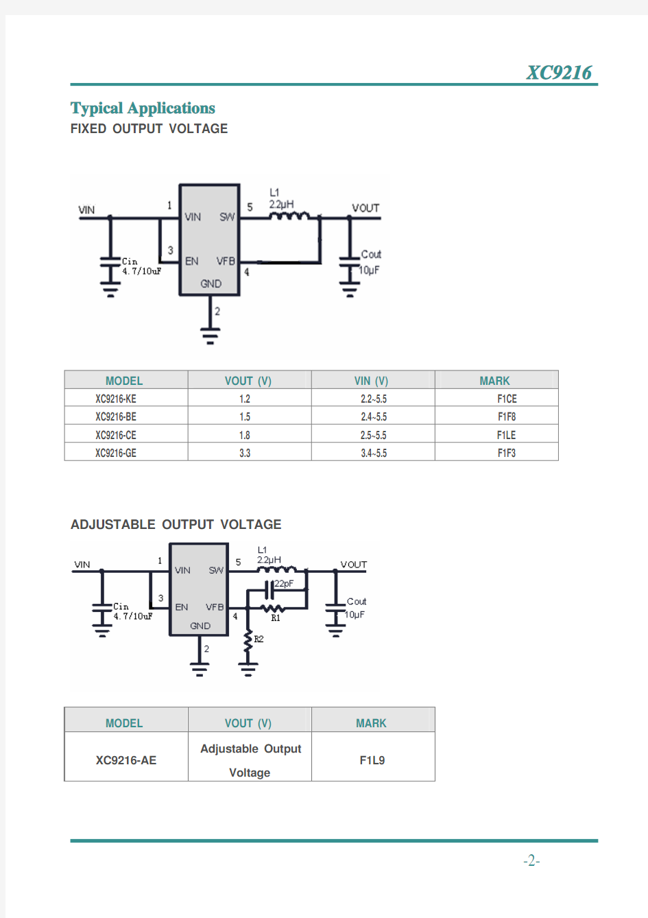
Typical Applications
FIXED OUTPUT VOLTAGE
XC9216
MODEL XC9216-KE XC9216-BE XC9216-CE XC9216-GE
VOUT (V) 1.2 1.5 1.8 3.3
ADJUSTABLE OUTPUT VOLTAGE
VIN (V) 2.2~5.5 2.4~5.5 2.5~5.5 3.4~5.5
MARK F1CE F1F8 F1LE F1F3
MODEL XC9216-AE
VOUT (V) Adjustable Output
Voltage
MARK F1L9
-2-
THE DEVICE RECOMMENDED
XC9216
VOUT (V)
CAPACITOR SIZE/TYPE
CIN(μF)
COUT(μF)
1.2 4.7/10(0805) 10(0805) 1.5 4.7/10(0805) 10(0805)
1.8 4.7/10(0805) 10(0805) 3.3 4.7/10(0805) 10(0805)
RESISTOR SIZE/TYPE
R2(K?)
100 (0805) 1000(0805) 200(0805) 330(0805)
R1(K?)
100 (0805) 620(0805) 100(0805) 75(0805)
INDUCTOR SIZE/TYPE
μ( H) μ CKH4B28-2.2 H μ CKH4B28-2.2 H μ CKH4B28-2.2 H μ CKH4B28-2.2 H
Pin Assignment
5
4
1
2
3
SOT-23-5
PIN NUMBER SOT-23- 5
1 2
PIN NAME
VIN GND
3
EN
4
VOUT
5
SW
FUNCTION
Input Ground ON/OFF Control (High Enable) Output Switch Output
-3-
Functional Diagram
XC9216
-4-
Absolute Maximum Ratings
XC9216
Power Dissipation………………………….…….…………………………Internally limited
~ VIN …………………………………..……………….……………………………..- 0.3 V + 6 V
~ VON/OFF ………………………………………………….…………………………- 0.3 V (VIN + 0.3) V
~ VSW ……………………………………..………………………………- 0.3 V (VIN + 0.3) V
~ V F B … … … … … … … … … … … … … . . … . … … … … … … … … … … . . . . . - 0 . 3 V
+6V
℃ ~ ℃ IS W ………………………………………….…………………..……………………………..1.3A
Operating Temperature Range ………………………………………...- 40
+ 85
℃ Lead Temperature (Soldering 10 sec.) …………………………………………………..+ 300
℃ ~ ℃ Storage Temperature Range ………………………..……………………….….- 65
+ 150
℃ Junction Temperature ……………………….…..………………..………………………+ 125
-5-
Electrical Characteristics
℃ Operating Conditions: TA=25 , VIN=3.6V unless otherwise specified.
XC9216
SYMBOL
PARAMETER
VOUT
Output Voltage
CONDITIONS I OUT = 100mA
MIN TYP MAX UNITS
1.75 1.80 1.85
V
VIN
Input Voltage Range
VFB
Regulated Voltage
℃ TA = 25
2.5
5.5
V
0.5880 0.6 0.6120 V
IFB
?VFB
Feedback Current VREF
VIN=2.5V~5.5V
±30
nA
0.03 0.4
%/V
FOSC IQ IS
Oscillator Frequency Quiescent Current Shutdown Current
VFB = 0.6V or VOUT = 100%
1.1
1.4
1.7
MHz
VFB = 0.5V or VOUT = 90%, ILOAD = 0A
230 300
μA
VEN = 0V, VIN = 4.2V
0.1
1
μA
IPK
Peak Inductor Current
VIN = 3V, VFB = 0.5V or VOUT = 90%,
0.75 0.9
1
A
Duty Cycle < 35%
RPFET RDS(ON) of P-Channel FET ISW = 100mA
0.4
0.5
?
RNFET RDS(ON) of N-Channel FET ISW = -100mA
0.35 0.45
?
*
EFFI
Efficiency
When connected to ext.
components
93
%
?VOUT VOUT Line Regulation
VIN=EN=3.6 V, IOUT=100mA VIN=2.5V~5.5V
0.03 0.3
%/V
VLOADREG VOUT Load Regulation
0.33
%
EFFI = [(Output Voltage × Output Current) / (Input Voltage × Input Current)] × 100%
-6-
Typical Performance Characteristis
VOUT=1.8V
VOUT=2.5V
XC9216
CONVERSION EFFICIENCY
100
90
EFFICIENCY(%)
80 70 60 50 40 30 20
10
0
1
10
100
1000
OUTPUT CURRENT
VIN=2.7V VIN=3.6V VIN=4.2V
100
90
80
EFFICIENCY
70 60 50 40 30
20
10
0
1
CONVERSION EFFICIENCY
10
100
OUTPUT CURRENT
1000
VIN=2.7V VIN=3.6V VIN=4.2V
VOUT 100mV/DIV AC COUPLED
VIN=3.6V VOUT=1.8V ILOAD=0mA
2ms/DIV
VOUT 10mV/DIV AC COUPLED
VIN=3.6V VOUT=1.8V ILOAD=200mA
200ns/DIV
-7-
Typical Performance Characteristis
Start –up from shutdown
XC9216
Quiescent Supply Current vs. Supply Voltage
Feed back Bias Current vs. Temp
-8-
Typical Performance Characteristis
Shutdown Current vs. Temp
XC9216
Switching Frequency vs. Temp
Rds(on) vs. Temp
Open/Closed Loop Current Limit vs. Temp
-9-
Application Information
XC9216
PIN ASSIGNMENT
VIN (Pin 1): Main Supply Pin. Must be closely decoupled to GND, Pin 2, with a 2.2μF or greater
ceramic capacitor.
GND (Pin 2): Ground Pin.
EN (Pin 3): En Control Input. Forcing this pin above 1.5V enables the part. Forcing this pin
below 0.3V shutsdown the device. In shutdown, all functions are disabled drawing <1μA supply current. Do not leave EN floating.
VOUT (Pin 4) (XC9216-BE/XC9216-CE): Output Voltage Feedback Pin. An internal resistive
divider divides the output voltage down for comparison to the internal reference voltage.
SW (Pin 5): Switch Node Connection to Inductor. This pin connects to the drains of the internal main and synchronous power MOSFET switches.
VFB (Pin 4) (XC9216-AE): Feedback Pin. Receives the feedback voltage from an external
resistive divider across the output. In the adjustable version, the output voltage is set by a resistive divider according to the following formula: VOUT = 0.6V ? [1 + (R1/R2)].
-10-
INDUCTOR SELECTION
XC9216
For most applications, the value of the inductor will fall in the range of 1μH to 4.7μH. Its value is chosen based on the desired ripple current. Large value inductors lower ripple current and small
△ value inductors result in higher ripple currents. Higher VIN or VOUT also increases the ripple
current as shown in equation 1. A reasonable starting point for setting ripple current is IL = 240mA (40% of 600mA).
The DC current rating of the inductor should be at least equal to the maximum load current plus half the ripple current to prevent core saturation. Thus, a 720mA rated inductor should be enough for
most applications (600mA + 120mA). For better efficiency, choose a low DC-resistance inductor. Different core materials and shapes will change the size/current and price/current relationship of an inductor. Toroid or shielded pot cores in ferrite or permalloy materials are small and don’t radiate much energy, but generally cost more than powdered iron core inductors with similar electrical characteristics. The choice of which style inductor to use often depends more on the price vs size requirements and any radiated field/EMI requirements than on what the HX1001 requires to operate. Table 1 shows some typical surface mount inductors that work well in HX1001 applications.
Table 1. Recommended Inductors
PART
CDRH3D16 CDH3B16
L (μH)
MAX
DCR
m?
2.2 75 2.2 70
MAX DC CURRENT
(A)
1.20 1.20
SIZE W×L×H
(mm3)
VENDOR
3.8 × 3.8 × 1.8 Sumida 4.0 × 4.0 × 1.8 Ceaiya
-11-
OUTPUT AND INPUT CAPACITOR SELECTION
XC9216
In continuous mode, the source current of the top MOSFET is a square wave of duty cycle VOUT/VIN. To prevent large voltage transients, a low ESR input capacitor sized for the maximum RMS current must be used. The maximum RMS capacitor current is given by:
This formula has a maximum at VIN = 2VOUT, where IRMS = IOUT/2. This simple worst-case condition is commonly used for design because even significant deviations do not offer much relief. Note that the capacitor manufacturer’s ripple current ratings are often based on 2000 hours of life. This makes it advisable to further derate the capacitor, or choose a capacitor rated at a higher temperature than required. Always consult the manufacturer if there is any question.
The selection of COUT is driven by the required effective series resistance (ESR).
Typically, once the ESR requirement for COUT has been met, the RMS current rating generally far
exceeds the IRIPPLE(P-P) requirement. The output ripple ?VOUT is determined by:
where f = operating frequency, COUT = output capacitance and ?IL = ripple current in the inductor. For a fixed output voltage, the output ripple is highest at maximum input voltage since ?IL
increases with input voltage.
Aluminum electrolytic and dry tantalum capacitors are both available in surface mount configurations. In the case of tantalum, it is critical that the capacitors are surge tested for use in switching power supplies. An excellent choice is the AVX TPS series of surface mount tantalum. These are specially constructed and tested for low ESR so they give the lowest ESR for a given volume. Other capacitor types include Sanyo POSCAP, Kemet T510 and T495 series, and Sprague 593D and 595D series. Consult the manufacturer for other specific recommendations.
-12-
Packaging Information
SOT-23-5 Package Outline Dimension
XC9216
Symbol
A A1 A2 b c D E E1 e e1 L
θ
Dimensions In Millimeters
Min
Max
1.050
1.250
0.000
0.100
1.050
1.150
0.300
0.500
0.100
0.200
2.820
3.020
1.500
1.700
2.650
2.950
0.950(BSC)
1.800
2.000
0.300
0.600
0°
8°
Dimensions In Inches
Min
Max
0.041
0.049
0.000
0.004
0.041
0.045
0.012
0.020
0.004
0.008
0.111
0.119
0.059
0.067
0.104
0.116
0.037(BSC)
0.071
0.079
0.012
0.024
0°
8°
-13-