Liquid silicate additive for alkaline texturing of mono-Si wafers to improve process bath lifetime and reduce IPA consumption
Prabir Kanti Basu n,Debajyoti Sarangi,Kishan Devappa Shetty,Mathew Benjamin Boreland
Solar Energy Research Institute of Singapore,National University of Singapore,7Engineering Drive1,Block E3A,#06-01,Singapore117574,Singapore
a r t i c l e i n f o
Article history:
Received3August2012
Received in revised form
18January2013
Accepted21January2013
Available online28February2013
Keywords:
Industrial monocrystalline silicon solar cell
Alkaline texturing
Potassium silicate additive
Bath lifetime
Weighted average re?ectance
a b s t r a c t
An improved texturing process is reported for industrial monocrystalline silicon wafers,which uses a
small amount of liquid potassium silicate as an additive to the conventional KOH/IPA texturing process.
The new silicate additive does not require any other changes to the chemical components and thus can
easily be integrated into the standard industrial process.Re?ectivity and scanning electron microscope
studies con?rm that the new process yields smaller pyramidal structures of about4–6m m in height,
with an improved uniformity across the entire Si surface resulting in a low solar weighted average
re?ectance(WAR)in the range11.4–12.2%.Moreover a near three-fold decrease in IPA consumption
and a six-fold increase in bath lifetime are achieved by the new texturing process compared to the
standard texturing process.For156mm?156mm pseudo-square CZ monocrystalline p-type silicon
wafers cell ef?ciencies of over18%are achieved with the new texturing process on industrial-grade,
screen-printed solar cells fabricated on SERIS’industrial R&D pilot line.This process offers the potential
for signi?cant cost reduction in manufacturing of monocrystalline silicon wafer solar cells.
&2013Elsevier B.V.All rights reserved.
1.Introduction
The use of anisotropic chemical texturing to reduce front
surface re?ectance loss is an essential step in the fabrication of
monocrystalline silicon wafer solar cells.However,high isopropyl
alcohol(IPA)consumption and limited chemical bath lifetimes
are signi?cant cost factors,which must be addressed to reduce
overall production costs.
For monocrystalline Si solar cells,sodium hydroxide(NaOH)or
potassium hydroxide(KOH)based solutions are used for aniso-
tropic selective etching of the/100S silicon surface to form a
textured surface of random upright pyramids.The textured sur-
face reduces optical re?ectance due to the so-called‘double-
bounce’effect[1–3].IPA is generally added to the alkaline
solution to achieve good lateral uniformity of the pyramids across
the Si wafer surface by modifying the surface wettability to
controllably nucleate the texturing process[4].
Etching bath temperatures of over801C are typically used to
minimise the process time.However,this process temperature is
above the boiling point of IPA,leading to high IPA consumption
due to evaporation.The high IPA usage is a signi?cant cost in the
texturing process,which increases the cost per watt-peak of the
solar cell.In addition,the reaction by-products in the texture
solution tend to de-stabilise the texturing process,which limits
the texturing bath life.The need for frequent replacement of the
texturing solution reduces the productivity of the texturing
solution,which further increases cost.Consequently signi?cant
reduction or elimination of IPA usage,without detrimental impact
on cell electrical performance,is a key focus area for research on
texturing processes.
Several researchers have tried to replace KOH/NaOH based
solutions with alternative chemical solutions including:tetra-
methyl ammonium hydroxide(TMAH)[5],tribasic sodium phos-
phate(Na3PO4,12H2O)[6],hydrazine mono-hydrate(N2H4,H2O)
[7],sodium carbonate/bicarbonate(Na2CO3/NaHCO3)[8].How-
ever,in each case IPA is still required for pyramid nucleation.
Moreover,using any of those new texture chemicals,to the best of
our knowledge,till date there are no reports of cells with418%
ef?ciency for standard full-area aluminium back surface?eld(Al-
BSF)large-area screen-printed solar cells.
Other researchers have investigated the use of additives to
reduce or eliminate IPA[9–16].It was shown by Lee et al.that the
addition of the chlorinated compound2,4,6-trichloro-1,3,5-tria-
zine to the NaOH solution generates a low average re?ectance of
$16%over the400–1100nm wavelength range and achieved
17.2%solar cell ef?ciency[9].However,the process time was
longer(35min)and the process formed undesirable larger pyr-
amids of47m m height.Sun and Tang[10]proposed the use of
sodium hypochlorite(NaOCl)to replace NaOH as texturing
chemical and they showed that this solution could lead to the
formation of small pyramids with heights$2m m and reported an
Contents lists available at SciVerse ScienceDirect
journal homepage:https://www.doczj.com/doc/4813033879.html,/locate/solmat
Solar Energy Materials&Solar Cells
0927-0248/$-see front matter&2013Elsevier B.V.All rights reserved.
https://www.doczj.com/doc/4813033879.html,/10.1016/j.solmat.2013.01.037
n Corresponding author.Tel.:t6594479063,t6566011739;
fax:t6567751943.
E-mail addresses:prabir.basu@https://www.doczj.com/doc/4813033879.html,.sg,
prabir_basu64@https://www.doczj.com/doc/4813033879.html,(P.K.Basu).
Solar Energy Materials&Solar Cells113(2013)37–43
average re?ectance of 10.8%over the 400–1000nm wavelength range.However,the usage of large amounts of ethyl alcohol (10%by volume)makes the process costlier and more hazardous compared to the standard KOH or NaOH process,making it impractical for industrial use.Birman et al.[11]developed a new recipe with a combination of KOH-1,4cyclohexanedial (CHX)for texturing.Wijekoon et al.[12]and Mayer et al.[13]used a polymer concentrate and aromatic compounds respectively in KOH solution for texturing of https://www.doczj.com/doc/4813033879.html,ing a combination of KOH with high boiling alcohol (HBA)Quiebras et al.[14]achieved 17.6%cell ef?ciency for industrial screen-printed solar cells.
Recently,equipment vendors like RENA GmbH [15]and Stangl GmbH [16]released commercial process tools for IPA-free textur-ing of monocrystalline silicon wafers.Some commercial chemical suppliers like Dow Chemical [17]and GP Solar [18]also released IPA-replacement additives.However,little detailed information has thus far been reported on these various technologies.
The present paper reports a new,low-cost approach for anisotropic c-Si texturing based on the inclusion of a new additive,potassium silicate (K 2SiO 3),to the conventional KOH-IPA based texturing process.We compared this new texturing process with the standard KOH-IPA texturing process [9].This new texturing process realised a lower weighted average re?ec-tance (WAR),which was reduced to $2%compared to a WAR value of $3%for the standard texturing process after application of an antire?ection coating (ARC).More importantly,the new additive achieved a near three-fold reduction in IPA consumption,increased the texturing bath’s throughput by a factor of $3and the bath life by 6times.The new texturing process was applied to fabricate industrial-grade,screen-printed solar cells on 156mm ?156mm pseudo-square CZ monocrystalline p-type silicon wafers,giving ef?ciencies of over 18%,which is better than the cells textured with the standard process.
2.Experimental 2.1.Texturisation
All the texturing and solar cell fabrication experiments were performed in batches of 50wafers using industrial grade mono-crystalline CZ silicon wafers (156mm ?156mm pseudo-square,boron doped,p-type,/100S orientation,0.5–3O -cm resistivity,
160–180m m thickness).Before texturing a pre-cleaning and damage removal process was applied,following the process developed by Basu et al.[19].This pre-cleaning and saw damage removal process used KOH (20%by weight)and NaOCl solution in a ratio of 1:3(by volume).A process time of 2min at 801C was used to remove $3m m of silicon per side from the wafers for saw damage removal as calculated from the weight loss of the wafers after the process.
The chemical bath (constructed from polyvinylidene di?uoride (PVDF)material)used for texturing was heated from the bottom by a ?at Te?on coated heater and the temperature of the texturing solution was maintained at a constant value of 801C.To minimise concentration and temperature gradients,the solu-tion was also circulated using an external pump connected to an over?ow weir at the top of the bath,which re-circulated the solution to the bottom of the bath,just below the heater.The amount of Si removed during the texturing process was calcu-lated by measuring the weight of the wafer before and after the texturing process.
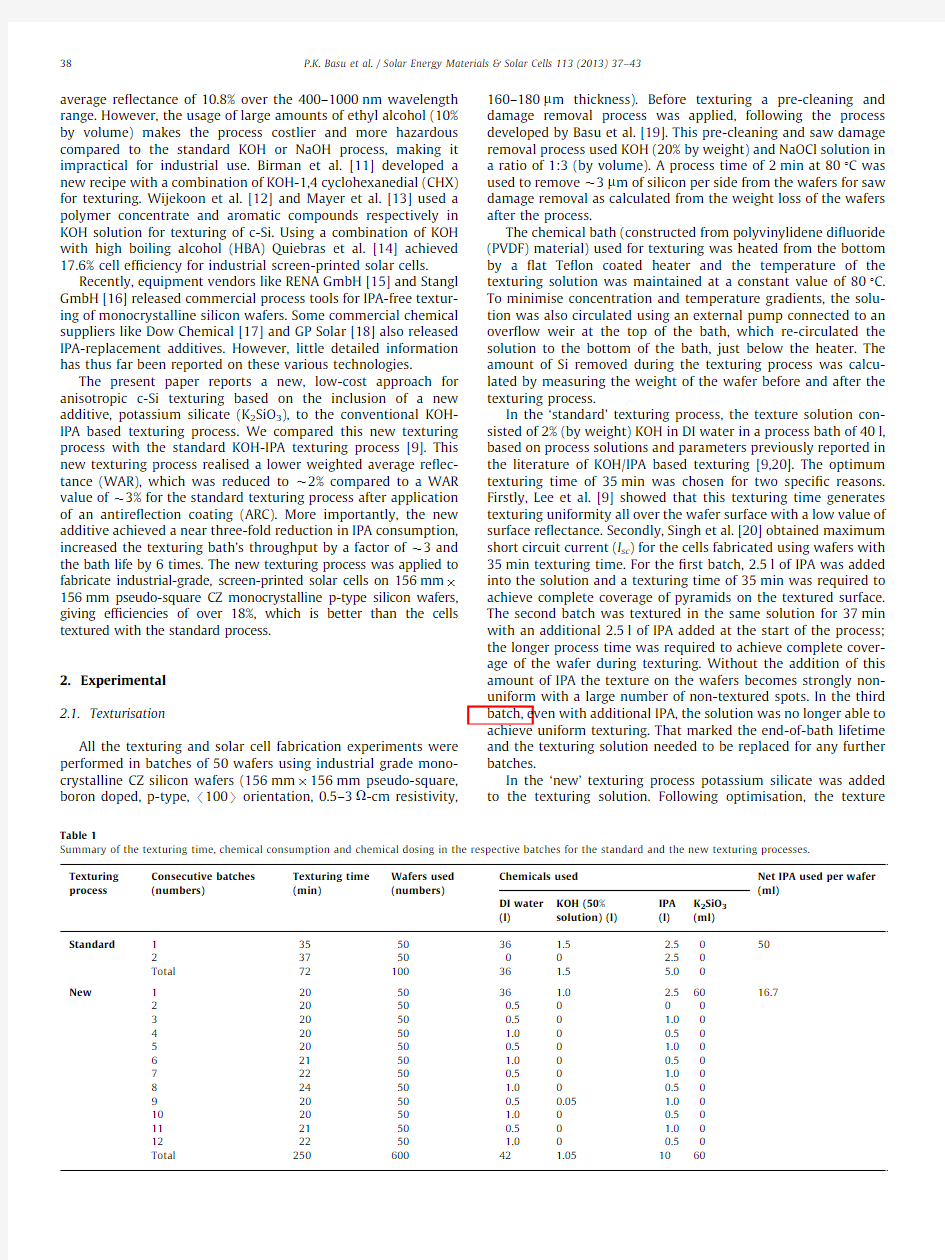
In the ‘standard’texturing process,the texture solution con-sisted of 2%(by weight)KOH in DI water in a process bath of 40l,based on process solutions and parameters previously reported in the literature of KOH/IPA based texturing [9,20].The optimum texturing time of 35min was chosen for two speci?c reasons.Firstly,Lee et al.[9]showed that this texturing time generates texturing uniformity all over the wafer surface with a low value of surface re?ectance.Secondly,Singh et al.[20]obtained maximum short circuit current (I sc )for the cells fabricated using wafers with 35min texturing time.For the ?rst batch,2.5l of IPA was added into the solution and a texturing time of 35min was required to achieve complete coverage of pyramids on the textured surface.The second batch was textured in the same solution for 37min with an additional 2.5l of IPA added at the start of the process;the longer process time was required to achieve complete cover-age of the wafer during texturing.Without the addition of this amount of IPA the texture on the wafers becomes strongly non-uniform with a large number of non-textured spots.In the third batch,even with additional IPA,the solution was no longer able to achieve uniform texturing.That marked the end-of-bath lifetime and the texturing solution needed to be replaced for any further batches.
In the ‘new’texturing process potassium silicate was added to the texturing solution.Following optimisation,the texture
Table 1
Summary of the texturing time,chemical consumption and chemical dosing in the respective batches for the standard and the new texturing processes.Texturing process
Consecutive batches (numbers)
Texturing time (min)
Wafers used (numbers)
Chemicals used Net IPA used per wafer (ml)
DI water (l)
KOH (50%solution)(l)IPA (l)K 2SiO 3(ml)Standard
1355036 1.5 2.5050
2375000 2.50Total 7210036 1.5 5.00New 1205036 1.0 2.56016.7
220500.5000320500.50 1.0042050 1.000.50520500.50 1.0062150 1.000.50722500.50 1.0082450 1.000.50920500.50.05 1.00102050 1.000.501121500.50 1.00122250 1.000.50Total
250
600
42
1.05
10
60
P.K.Basu et al./Solar Energy Materials &Solar Cells 113(2013)37–43
38
solution composition was changed to a lower KOH concentration of 1.4%(by weight)with the addition of 60ml of potassium silicate.The additive was added only during the initial makeup of the texturing solution.For the ?rst texturing batch of 50wafers,2.5l of IPA was added for 20min of texturing time.Different amounts of KOH,IPA and DI water were subsequently added via dosing to maintain the texturing uniformity (see Table 1).A total of 12consecutive batches were textured in the same solution,demonstrating a signi?cant increase in bath lifetime.
After texturing,all the wafers were neutralised in 50%hydro-chloric (HCl)acid solution at 601C for 10min followed by a dip in dilute hydro?uoric acid (HF).The complete process ?ow for the standard and the new process is shown in Fig.1.Following texturing the wafers were processed together as a single batch.2.2.Cell fabrication
The textured wafers were diffused in a tube diffusion furnace (TS81004,Tempress)using POCl 3as the dopant source with a target sheet resistance of 70O /sq.The ?nal sheet resistance after the diffusion was con?rmed by four-point-probe measurements (Cresbox,NAPSON).The parasitic rear-junction and the front phosphosilicate glass (PSG)were removed in an industrial inline etching tool (InPilot,RENA GmbH)using solutions of HF–HNO 3–H 2SO 4and dilute HF,respectively.The SiN x passivation and antire?ection layer was deposited by PECVD (Roth &Rau,SiNA-XS)with a thickness of $70nm and a refractive index of 2.05at https://www.doczj.com/doc/4813033879.html,stly,front and rear contacts were formed by screen printing (PVP1200,DEK)and subsequently co-?red in an indus-trial fast ?ring furnace (Ultra?ex,Despatch).The metallisation pastes used were Cermet SOLUS 6214and DuPont PV159A for the
rear aluminium (Al)and front silver (Ag),respectively.The complete cell fabrication process ?ow is shown in Fig.2.2.3.Characterisation
Representative sample wafers for the standard and new texturing processes were removed from the process for surface and re?ectivity characterisation studies.Prior to the measure-ments,the representative samples were cleaned in IPA,followed by DI rinsing and drying.A scanning electron microscope (Carl Zeiss Auriga)was used for the surface studies and a spectro-photometer (Perkin Elmer,Lambda 950)was used for the re?ec-tance studies.For calculation of the WAR,the diffuse re?ectance of the textured surfaces was measured using a 150mm diameter integrating sphere over the wavelength range of 300–1000nm.The illuminated I–V characteristics of the solar cells were mea-sured on a super class-A solar simulator (AESCUSOFT,SolSim 210)under standard testing conditions (STC).3.Results and discussions 3.1.Texturing results
The chemical reaction for KOH texturisation is [11]:Si t2KOH -K 2SiO 3t2H 2:
e1T
Following Eq.(1),during the texturing reaction,evolution of hydrogen (H 2)bubbles occurs.These H 2bubbles tend to stick to the Si surface and thus mask the surface locally.This leads to non-texturing at the masked spots and ?nally results in non-uniform texturing over the Si surface.The role of IPA is to prevent H 2bubble formation on the Si surface by enhancing Si surface
Fig.1.Process ?ow diagrams of the standard and the new texturing processes.For the new process,the modi?ed texture recipe is shown as dashed box.
Fig.2.Schematic illustration of the solar cell processing ?ow used in this work.
P.K.Basu et al./Solar Energy Materials &Solar Cells 113(2013)37–4339
wettability.The effective removal of H2bubbles from the entire Si wafer surface maintains a consistent chemical reaction across the whole Si wafer surface and in this way a uniform texturing can be obtained.
Faster process times can be achieved by increasing the KOH concentration to increase the etching rate.From Eq.(1)it is clear that a higher KOH concentration also results in the formation of more H2and thereby increases the usage of IPA required to minimise the adverse effect of the H2bubbles.However,the higher KOH concentration also tends to result in the formation of irregularly placed large pyramids depending on local/100S Si etching conditions.Simultaneously,the increased KOH concen-tration raises the concentration of K2SiO3in the solution due to the chemical reaction in Eq.(1).The increased concentration of the K2SiO3reaction by-product progressively slows down the Si etch rate[11]by the reduction of active KOH present in the texture solution thereby pushing solution concentrations into a different process window and destabilising the texturing process. Thus the etching rate and stability of the texturing solution is rapidly reduced eventually leading to uncontrolled non-uniformity in texturing,namely,incomplete coverage of the pyramidal textured surface and wide variation in pyramid size, which marked the end-of-bath lifetime.
After?rst batch of texturing in the‘standard’solution with a process time of35min,the etch rate of the solutions reduces due to increasing K2SiO3formation.Consequently the process time was increased in the second batch to compensate for the lower etch rate in order to achieve complete coverage of the texturing of the silicon surface.However,by the third batch,the etch rate became so low that complete coverage could not be achieved even after40min of texturing time.So the end-of-bath lifetime occurred with our standard texturing process[9]after only two consecutive batches of texturing.Industrially,such premature bath failure can be delayed reducing the loading factor of wafers in the solution(e.g.200wafer batch sizes for a400l of process solution volume on an industrial tool against50wafer batch sizes in a40l of process solution volume on our laboratory scale bath). The lower number of wafers per litre of texture solution slows the batch-to-batch increase in K2SiO3concentration,enabling a longer bath lifetimes.However,as will be shown later in the paper,bath lifetime can be signi?cantly increased without the need to reduce the bath loading factor by using liquid silicate solutions to control the process.
Crushed silicon is commonly added to texturing baths to ‘‘initialise’’the solution by raising dissolved Si concentration (i.e.silicates)by chemical reaction in the solution in an attempt to change the concentration of reactants and products into a more stable process window.However,the dynamic nature of the chemical reaction in Eq.(1)makes process control more challen-ging.In the new process we use a liquid K2SiO3solution in the initial bath make-up,which enables us to directly manipulate the silicate concentration and thus avoid the dif?culties of the dynamic chemical reaction.In this way we can more accurately adjust the relative starting concentrations of reactants and pro-ducts to reach a more stable and controllable texturing process window.
In our new texturing process we mixed an optimised amount (60ml)of K2SiO3in the initial bath make-up of KOH(1.4% concentration by weight)and2.5l IPA.The initial quantity of silicate and a relatively low KOH concentration(as compared to the standard process)moderated Si etch rate to a large extent. Consequently the generation of H2bubbles was reduced,in turn reducing the requirement for IPA.Silicate generation was also reduced,increasing the bath stability.All these effects combined allowed us to perform texturing with small and regular pyramids for a larger number of consecutive batches with little or no dosing of KOH,IPA and DI water.It should be noted that K2SiO3was only added during the initial bath make up with no subsequent dosing. For the?rst?ve consecutive batches,constant dosing of IPA and DI water was used to maintain a?xed20min texturing time.For the sixth batch to eighth batch,the texturing time was increased slightly to a maximum of24min to compensate for the slowing of the texturing rate in order to maintain a complete texturing.An addition of50ml of KOH solution at the end of the8th batch was used to increase the active KOH concentration and re-set the texturing time to20min for the ninth and tenth batches.The texturing time was again increased for the eleventh and twelfth batch,again to maintain completeness and uniformity of the texturing,suggesting the onset of the end-of-bath lifetime.The end-of-bath lifetime was reached at the thirteenth batch when we found the texturing solution was too weak to achieve complete texturing even with a texturing time of up to30min. We did not try texturing for more than30min as our objective was to keep the process time within30min.The usage of chemicals and texturing time for each batch,for both the standard and new texturing processes,is listed in Table1.
The relative uniformity of texturing and pyramid size is evident in the plan-view SEM micrographs of Fig.3.For the Si wafer textured with the standard process(Fig.3(a)),we clearly observe$5-10m m wide pyramids distributed over the Si surface. By comparison,for the Si wafer textured with the new process (Fig.3(b)),the surface has signi?cantly smaller pyramids in the $3–6m m range with improved uniformity particularly in regards to the reduced incidence of very large pyramids.Moreover,
the
Fig.3.SEM micrograph(planar view,magni?cation?2000?)of a textured wafer fabricated using the(a)standard texturing process and(b)the new texturing process.
P.K.Basu et al./Solar Energy Materials&Solar Cells113(2013)37–43 40
standard process shows fewer numbers of complete pyramids and a higher number of overlapping pyramids.In the oblique SEM micrographs (2000?magni?cation)of the textured wafers,for the standard process (Fig.4(a)),several pyramids with heights 48m m were observed,whereas for the new process (Fig.4(b))pyramids with heights 46m m were not observed.Overall,the SEM images clearly demonstrate that the new texturing process reduces the pyramid size,with a simultaneous improvement in uniformity as compared to the standard texturing process.
The Si etch rate for both the standard and new texturing processes were studied to understand the relationship between the weakening of the respective baths during consecutive textur-ing batches.The amount of Si removed for each texturing batch is shown in Fig.5.
In the standard texturing process the amount of Si removal per wafer per side ($11-12m m)is nearly double that of the new process ($4-6m m).According to Eq.(1),the larger amount of etched Si in the standard process consequently results in a more rapid increase in silicate concentration in the solution,which in turn accelerates the reduction in the texturing rate and bath stability.Thus after only the second batch of texturing,the standard texturing solution falls out of process and fails to yield a regular pyramid structure.However,for the new process the lower Si removal per batch enables the texturing bath to remain in the stable process window for a larger number of consecutive texturing batches.Simultaneously,a lower Si removal rate also minimises the H 2production,which in turn reduces the require-ment for IPA.
Achieving low WAR values with batch-to-batch repeatability for the textured surface is equally important from the point of
view of photocurrent generation.The batch-to-batch variation of WAR values for the standard and new processes is shown in Fig.6.The batch-to-batch variation is generally very low for the new process,with only batches 1,8and 12showing moderately higher WAR values (12.1%,12.0%and 12.1%,respectively),which is nevertheless much smaller than the WAR values (12.9%and 13.1%)achieved using the standard texturing process.
The spectral re?ectance curves for the textured wafers before and after SiN x deposition (see Fig.7)further con?rm improved optical properties for the new process,as the re?ectance loss for the new process is lower at all wavelengths.3.2.Solar cell results
The one-sun I–V curves of the best solar cells fabricated from both types of textured wafers are shown in Fig.8.As expected,the short-circuit current density (J sc )is improved using the
new
Fig.4.SEM micrograph (view angle of 451,magni?cation ?2000?)of a textured wafer fabricated using the (a)standard texturing process and (b)the new texturing
process.
Fig.5.Graph indicating the variation of the amount of Si thickness etched per wafer side for consecutive batches using the standard and the new texturing
processes.
Fig.6.Graph indicating the variation of weighted average re?ectance (WAR)with the corresponding batch numbers textured in the baths using the standard and new texturing processes.
P.K.Basu et al./Solar Energy Materials &Solar Cells 113(2013)37–4341
process due to its lower WAR value.However the reasons of the improved open-circuit voltage (V oc )and ?ll factor (FF)are less obvious.The higher FF of 79.3%for the cell using the new process could be due to improved continuity of the front metal ?ngers resulting from the smaller and more uniform pyramids [17].3.3.Chemical usage results
Table 1summarises the usage of chemicals,including dosing,for the standard and new texturisation processes.The new process achieved a signi?cant reduction in the chemical con-sumption per wafer.In particular the net IPA consumption per wafer was reduced from 50ml in the standard process to 16.7ml in the new process.This is a $3times reduction in IPA consump-tion,which is one of the costliest liquid chemicals used in the
silicon PV industry.Moreover,the amount of the K 2SiO 3additive required to achieve the IPA savings is so small that the additional cost is comparatively negligible (at current prices the silicate cost was $0.50US$for texturing 600wafers).
Table 2shows the productivity of the texturing processes in terms of net throughput.All the individual process steps includ-ing the solution preparation,heating times and post-texturing cleaning steps (i.e.neutralization,HF dip,DI rinse and drying)were accounted for.A 2.8times increase in throughput was achieved,for our tool con?guration,using a relatively small 40l process bath with a high wafer loading (i.e.,only 0.80l/wafer).The increased throughput is due to the six times longer bath lifetime and the 40%reduction of the average texturing process time from 35min to 21min.
4.Conclusion
An improved silicon wafer texturing process using a liquid potassium silicate additive was developed,which provides sig-ni?cant cost reduction potential without compromising solar cell performance.In particular a near three-fold reduction of IPA consumption and three-fold increase in process throughput has been achieved,combined with a six-fold increase in end-of-bath lifetime.Moreover,transfer of the new process to existing industrial process tools does not require signi?cant hardware changes,due to the very small quantities of potassium silicate required.The new process not only improves the stability and productivity of the texturisation bath,but also yields improved solar cell ef?ciencies,as demonstrated by ef?ciencies of up to 18.3%for industry-standard screen-printed silicon wafer solar cells.
Acknowledgement
The authors thank their colleagues from the Silicon Photo-voltaics Cluster of the Solar Energy Research Institute of Singa-pore (SERIS)for their assistance in sample processing and characterisation.SERIS is sponsored by the National University of Singapore (NUS)and Singapore’s National Research Foundation (NRF)through the Singapore Economic Development Board (EDB).References
[1]F.Restrepo,C.E.Backus,On black solar cells on the tetrahedral texturing of a
silicon surface,IEEE Transactions on Electron Devices ED-23(1976)1193–1195.
[2]E.D.Palik,O.J.Glembocki,I.Heard Jr.,P.S.Burno,L.Tenerz,Etching roughness
for (100)silicon surfaces in aqueous KOH,Journal of Applied Physics 70(1991)
3291–3300.
Fig.7.Measured spectral hemispherical re?ectance of wafers textured using the standard and the new texturing process,before and after ARC SiN x deposition.The weighted average re?ectance (WAR)is weighted using the AM1.5G solar spectrum over the 300–1000nm wavelength
range.
Fig.8.Measured one-sun I–V characteristics of the best solar cells fabricated using the standard and new texturing processes.The best cells processed with the standard and new texturing processes achieved 17.7%and 18.3%ef?ciency,respectively.
Table 2
Comparison of the process times of the standard and the new texturing processes.
Texturing process Standard
New Bath lifetime (batches)212Bath preparation time (min)6060Actual texturing time of complete batches (min)72250Total numbers of wafers textured 100600Post-texture clean Neutralisation and DI rinse (min)15
15Final HF dip,DI rinse and dry (min)1010Total process time (min)
157335Net throughput (wafers per hour)
38
107
P.K.Basu et al./Solar Energy Materials &Solar Cells 113(2013)37–43
42
[3]Q.B.Vu,D.A.Stricker,P.M.Zavracky,Surface characteristics of(100)silicon
anisotropically etched in aqueous KOH,Journal of the Electrochemical Society 143(1996)1372–1375.
[4]P.Verlinden,O.Evrard,E.Mazy,A.Crahay,The surface texturization of solar
cells:a new method using V-grooves with controllable sidewall angles,Solar Energy Materials and Solar Cells26(1992)71–78.
[5]A.Merlos,M.Acero,M.H.Bao,J.Bausells,J.Esteve,TMAH/IPA anisotropic
etching characteristics,Sensors and Actuators A37–38(1993),pp.737–743.
[6]U.Gangopadhyay,K.H.Kim,S.K.Dhungel,U.Manna,P.K.Basu,M.Banerjee,
H.Saha,Yi Junsin,A novel low cost texturization method for large area
commercial mono-crystalline silicon solar cells,Solar Energy Materials& Solar Cells90(2006)3557–3567.
[7]U.Gangopadhyay,K.Kim,S.K.Dhungel,P.K.Basu,J.Yi,Low-cost texturization
of large-area crystalline silicon solar cells using hydrazine mono-hydrate for industrial use,Renewable Energy31(2006)1906–1915.
[8]A.Montesdeoca-Santana,E.Jimenez-Rodriguez,B.Gonzalez-Diaz,D.Borchert,
R.Guerrero-Lemus,Ultra-low concentration Na2CO3/NaHCO3solution for textur-ization of crystalline silicon solar cells,Progress in Photovoltaics:Research and Applications20(2012)191–196.
[9]J.Lee,https://www.doczj.com/doc/4813033879.html,kshminarayan,S.K.Dhungel,K.Kim,J.Yi,Optimization of
fabrication process of high ef?ciency and low cost crystalline silicon solar cell for industrial applications,Solar Energy Materials and Solar Cells93 (2009)256–261.
[10]L.Sun,J.Tang,A new texturing technique of monocrystalline silicon surface
with sodium hypochlorite,Applied Surface Science255(2009)9301–9304.
[11]K.Birmann,M.Zimmer,J.Rentsch,Fast alkaline etching of monocrystalline
wafers in KOH/CHX,in:Proceedings of the23th European Photovoltaic Solar Energy Conference and Exhibition(EU PVSEC),Valencia,2008,pp.1608–1611.
[12]K.Wijekoon,T.Weodman,S.Paak,K.M.Williams,Production ready novel
texture etching process for fabrication of single crystalline silicon solar cells,
in:Proceedings of the35th IEEE Photovoltaic Specialists Conference(PVSC), Honolulu,HI,2010,pp.3635–3641.
[13]K.Mayer,T.Orellana Pe′rez,M.Rostas,M.Schumann,F.Granek,S.W.Glunz,E.
Rosenfeld,D.Kray,H.Antoniadis,Aromatic compounds as substitutes for 2-propanol as texturing additive in aqueous alkaline solutions,in:Proceedings of the25th European Photovoltaic Solar Energy Conference and Exhibition (EU PVSEC),Valencia,2010,pp.2511–2515.
[14]N.Ximello Quiebras,J.Junge,S.Seren,G.Hahn,E.Epple,Up to20%ef?cient
solar cells on monocrystalline silicon wafers by using a KOH—high boiling alcohol(HBA)texturing solution,in:Proceedings of the26th European Photovoltaic Solar Energy Conference and Exhibition(EU PVSEC),Hamburg, 2011,pp.849–852.
[15]/https://www.doczj.com/doc/4813033879.html,/?leadmin/img/Produkte/200_Solartechnik/
230_Batch/232_BatchTex/RENA_DB_monoTex_20110829_?nal.pdf S.
[16]/http://www.stangl.de/uploads/tx_pspublications/MetaTex200_06.
pdfhttp://www.stangl.de/uploads/tx_pspublications/MetaTex200_06.pdf S. [17]M.Moynihan, C.O’Connor, B.Barr,S.Tiffany,W.Braun,G.Allardyce,
J.Rentsch,K.Birmann,IPA free texturing of mono-crystalline solar cells,in: Proceedings of the25th European Photovoltaic Solar Energy Conference and Exhibition(EU PVSEC),Valencia,2010,pp.1332–1336.
[18]/http://www.gpsolar.de/en/materials/chemicals/gp-alka-tex-zero/S.
[19]P.K.Basu,H.Dhasmana,N.Udayakumar,F.Khan,D.K.Thakur,Regulated low
cost pre-treatment step for surface texturization of large area industrial single crystalline silicon solar cell,Solar Energy Materials and Solar Cells94 (2010)1049–1054.
[20]P.K.Singh,R.Kumar,https://www.doczj.com/doc/4813033879.html,l,S.N.Singh,B.K.Das,Effectiveness of anisotropic
etching of silicon in aqueous alkaline solutions,Solar Energy Materials and Solar Cells70(2001)103–113.
P.K.Basu et al./Solar Energy Materials&Solar Cells113(2013)37–4343
盘点虎牙直播实力主播首位叫板王者荣耀职业战队王者荣耀有多火就意味着王者荣耀的直播有多受欢迎。除了玩家们耳熟能详的嗨氏、裴小峰之外,虎牙直播还有一群犀利无比的王者荣耀主播,如果将这些主播凑成一个队伍,他们的阵容实力根本不虚职业队伍。究竟这些能够媲美职业选手的主播们是何方神圣,让我们一起来看下吧。 实力貂蝉:九日 作为虎牙直播的实力主播,九日的貂蝉和嗨氏同属于国服最强貂蝉系列。嗨氏的貂蝉更追求的是一张循序渐进的打法,而九日的貂蝉却往往喜欢在刀尖上跳舞,团战中锁定对方主力,在力求追杀对方伤害来源的情况下闪转腾挪,保证了貂蝉的存活率。这位百星王者的不知火舞也是一样的飘逸,操作与技术着实让人折服。除了直播中的实力,九日还在仙阁夺冠后的仙阁挑战赛中打败过仙阁的主力小羽,一时之间传为佳话。 死神露娜:曹操大表哥 虽然名为曹操大表哥,但大表哥最让人记住的英雄却是露娜。众所周知,由于露娜技能设定的原因,露娜一般选择的只有一去无归的刺客路线,但在曹操的手下,露娜的生存能力大大的得到 拓展,大招几近无限刷新的流氓打法也让他的貂蝉在钻石王者领域横冲霸道,喜欢露娜的玩家们可以观摩下这位主播的操作。
灭世孙尚香:李太白 除了本命英雄李白的神级实力,作为虎牙第一孙尚香,李太白对于孙尚香的了解超出常人。孙尚香机动性强且在团战中总能打出爆发伤害。但孙尚香也存在着容易被敌方突进和血量较低的缺点,李太白依靠一技能翻滚突袭的风骚走位经常在团战中上演极限反杀的表现。同时,由于自己打出来成吨的伤害,这位胖子主播也成功和李白的潇洒绝缘,给玩家们带来各种杀伐果决的操作后,继续搜寻着下一个猎物。 双英雄制霸:成成 在别的主播擅长的大多是一个英雄的时候,成成的嬴政和赵云给足了玩家们看点。曾经的虎牙第一猴王早已经不再满足于大闹天空,不管是前期给力的赵云还是后期发威的嬴政,成成能否信手拈来。作为王者荣耀明星导师的成成在直播时总会交给玩家们一些骚套路,这也是为什么他的赵云总能七进七出不死嬴政暗处放大豪取五杀。