FPGA课程设计实验报告
题目:VHDL编写的数字钟设计
学院:电子信息学院
专业:电子与通讯工程
姓名:朱振军
基于FPGA的VHDL数字钟设计
一、功能介绍
1.在七段数码管上具有时--分--秒的依次显示。
2.时、分、秒的个位记满十向高位进一,分、秒的十位记满五向高位进一,小时按24进制计数,分、秒按60进制计数。
3.整点报时,当计数到整点时扬声器发出响声。
4.时间设置:可以通过按键手动调节秒和分的数值。此功能中可通过按键实现整体清零和暂停的功能。
5.LED灯循环显示:在时钟正常计数下,LED灯被依次循环点亮。
待增加功能:
1.实现手动调节闹铃时间,在制定时间使扬声器发声。
2.实现微妙的快速计数功能,可实现暂停、保存当前时间、继续计数的功能。
二、设计方案
本文数字钟的设计采用了自顶向下分模块的设计。底层是实现各功能的模块,各模块由vhdl语言编程实现:顶层采用原理图形式调用。其中底层模块包括秒、分、时三个计数器模块、按键去抖动模块、按键控制模块、时钟分频模块、数码管显示模块共7个模块。
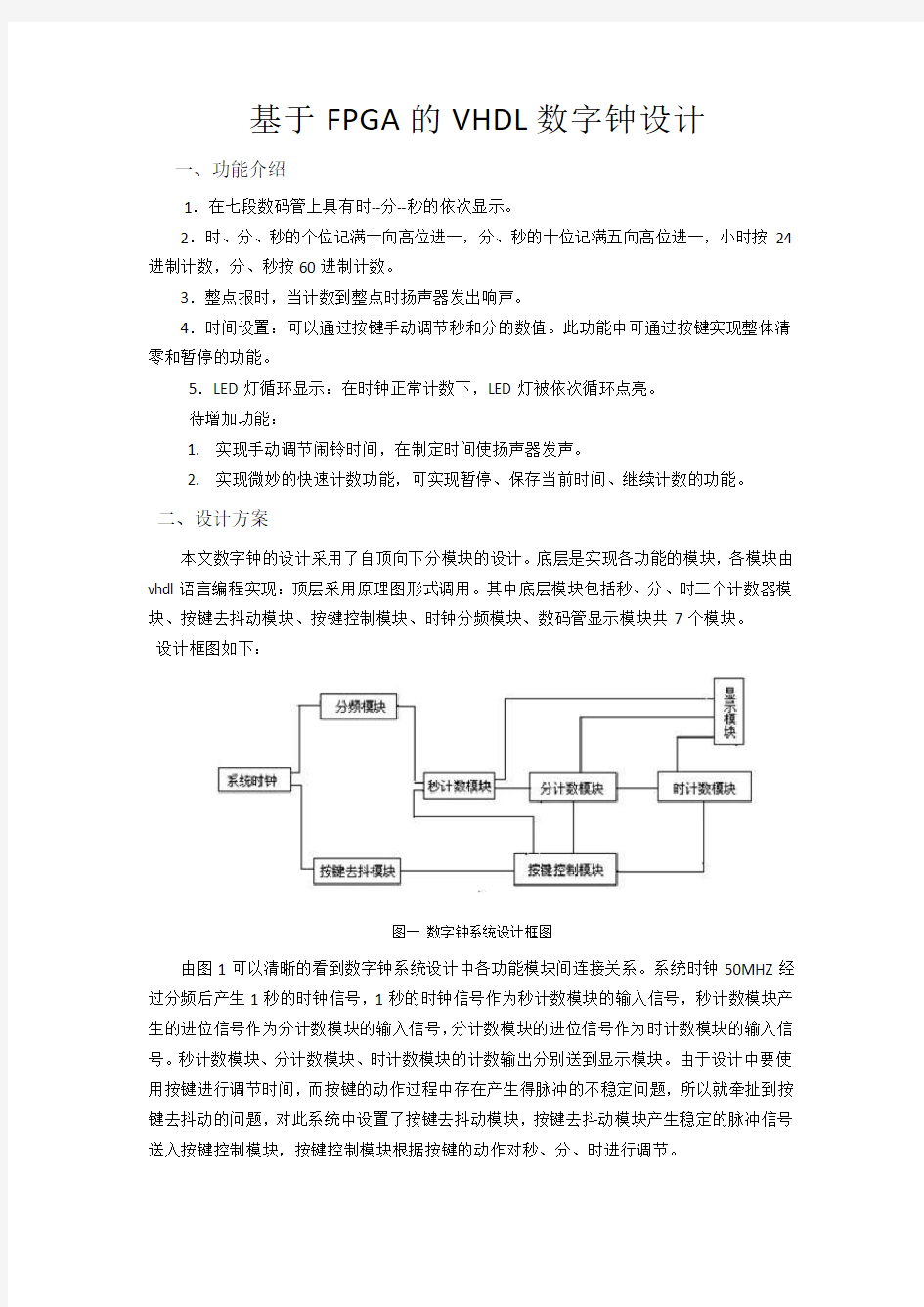
设计框图如下:
图一数字钟系统设计框图
由图1可以清晰的看到数字钟系统设计中各功能模块间连接关系。系统时钟50MHZ经过分频后产生1秒的时钟信号,1秒的时钟信号作为秒计数模块的输入信号,秒计数模块产生的进位信号作为分计数模块的输入信号,分计数模块的进位信号作为时计数模块的输入信号。秒计数模块、分计数模块、时计数模块的计数输出分别送到显示模块。由于设计中要使用按键进行调节时间,而按键的动作过程中存在产生得脉冲的不稳定问题,所以就牵扯到按键去抖动的问题,对此系统中设置了按键去抖动模块,按键去抖动模块产生稳定的脉冲信号送入按键控制模块,按键控制模块根据按键的动作对秒、分、时进行调节。
图二数字钟的顶层设计原理图
三、设计过程
由数字钟的顶层设计原理图可知:系统的外部输入即为系统的时钟信号CLK =50MHZ,系统的外部输出有蜂鸣器信号buzzer,LED显示信号LED[3..1]和shan(与按键去抖动模块的o3相连),数码管显示信号xianshi[7..0],数码管位选信号xuanze[7..0]。
下面将对内部功能模块进行详细说明;
1.分频模块pinlv
对系统的时钟50MHZ进行分频,设置不同长度的计数值,当系统时钟clk有变化时计数器开始计数,当计数到某个值时输出一个信号,计数值不同输出信号的周期也就不同,从而实现了对系统时钟进行不同的分频,产生不同频率的信号。
由VHDL语言生成的模块图和程序说明如下:
图三分频模块
library ieee;
use ieee.std_logic_1164.all;
use ieee.std_logic_unsigned.all;
entity pinlv is
port( clk:in std_logic;--系统时钟输入端口
clk2ms:out std_logic;
clk500ms:out std_logic;
clk1s:out std_logic);--各频率信号的输出端口
end;
architecture beh of pinlv is
begin
p1:process(clk) –进程p1
variable count1:integer range 0 to 49999999; begin
if(clk'event and clk='1')then count1:=count1+1;--在clk 的上升沿计数
if count1<=24999999 then clk1s<='0';
elsif count1<=49999999 then clk1s<='1'; else count1:=0;
--产生周期为1s的时钟信号
end if;
end if;
end process p1;--结束进程p1
p2:process(clk)—进程p2
variable count2:integer range 0 to 99999; begin
if(clk'event and clk='1')then count2:=count2+1;--在clk上升沿计数
if count2<=49999 then clk2ms<='0';
elsif count2<=99999 then clk2ms<='1';
--产生周期为2ms的扫描信号
end if;
end if;
end process p2;--结束进程p2
p3:process(clk)—进程p3
variable count3:integer range 0 to 24999999;
begin
if(clk'event and clk='1')then count3:=count3+1;在clk上升沿计数
if count3<=12499999 then
clk500ms<='0';
elsif count3<=24999999 then clk500ms<='1';
else count3:=0;
产生周期为500ms的时钟信号end if;
end if;
end process p3; end beh;
2.按键去抖动模块qudou
本设计用到FPGA开发板上的四个按键,由于按键有反应时间、抖动的问题,可能当按键被按一次时而系统感应到几次,造成误差。所以应该进行按键消抖的处理,让每按一次键系统只感应到一次按键。可以采用软件延时,触发反相器等方式进行消除抖动,本设计中采用软件延时的方式。
由VHDL语言生成的模块图和程序说明如下:
图四按键去抖动模块
library ieee;
use ieee.std_logic_1164.all;
use ieee.std_logic_unsigned.all;
entity qudou is
port(clk,k1,k2,k3,k4:in std_logic;
o1,o2,o3,o4:out
std_logic);--设置按键输入信号输出端口end;
architecture beh of qudou is
begin
process(clk,k1,k2,k3,k4)
variable cant1:integer;
variable cant2:integer;
variable cant3:integer;
variable cant4:integer;
begin
if clk'event and clk='1' then
if k1='1' then cant1:=0;
end if;--设置计数初值
if k2='1' then cant2:=0;
end if; --设置计数初值
if k3='1' then cant3:=0;
end if;
if k4='1' then cant4:=0;
end if; --设置计数初值
if cant1>2499999 then o1<='0';
else o1<='1';--延时0.5s
end if;
if cant2>2499999 then o2<='0';
else o2<='1'; --延时0.5s
end if;
if cant3>2499999 then o3<='0'; else o3<='1'; --延时0.5s
end if;
if cant4>2499999 then o4<='0'; else o4<='1'; --延时0.5s
end if;
cant1:=cant1+1; --加一计数
cant2:=cant2+1; --加一计数
cant3:=cant3+1; --加一计数
cant4:=cant4+1; --加一计数
end if;
end process;
end beh;
--设置计数初值
在quartus II 开发环境中进行仿真验证
图五 按键去抖动仿真效果图
由于0.5s 太长,在本仿真中设置了很小的一个量10clk ,从图中可以看出基本实现了按键去抖动的效果。无论按键怎么抖动,输出总是保持稳态10clk ,当下一个触发来了以后,就可以触发单稳态。
3,按键控制模块self1
本设计中使用了两个按键进行对时钟的暂停和调秒操作,当ok2按下时时钟暂停,再按ok3则进行秒个位的加一计数,每按一次进行加一处理。当调节好时间后,在按ok2键重新开始计数。
由VHDL 语言生成的模块图和程序说明如下:
图六 按键控制模块
library ieee;
use ieee.std_logic_1164.all; use ieee.std_logic_unsigned.all; entity self1 is port( c:in std_logic;
ok2:in std_logic;
ok3:in std_logic; ck:out std_logic); end ;--设置端口
architecture bea of self1 is signal m:std_logic; signal t:std_logic;
begin
p1:process(ok2,ok3,c)—ok2和ok3触发进程
begin
if ok2'event and ok2='0' then m<=not m;--由ok2 的动作产生m 的电平信号 end if;
if m='1' then ck<=not(ok3);--把按键ok3的脉冲信号给输出
else ck<=c;--否则把正常计数时钟给输出
end if;
end process p1;--结束进程 end bea;
4,秒、分六十进制模块cantsixty
本设中秒、分的六十进制是由个位的十进制和十位的六进制进行组合实现的。当个位记到9时自动向高位进一,同时个位自动清零。当十位记到5并且个位记到9时,
自动产生一
个进位脉冲,同时个位和十位分别从零开始重新计数。
由VHDL 语言生成的模块图和程序说明如下:
图七 六十进制模块
library ieee;
use ieee.std_logic_1164.all; use ieee.std_logic_unsigned.all; entity cantsixty is
port(clk:in std_logic; reset:in std_logic;
out1:out std_logic_vector(3 downto 0);
out2:out std_logic_vector(3 downto 0);
c:out std_logic); end;
architecture beh of cantsixty is signal ss1,ss2:std_logic_vector( 3 downto 0);
begin
p1:process(clk,reset) begin
if(reset='0')then
ss1<="0000";ss2<="0000";
elsif(clk'event and clk='1')then if ss1="1001" and ss2="0101" then c<='1';--当计数到59时产生进位信号 else c<='0';--否则不产生 end if;
if ss1="1001" then ss1<="0000"; if ss2="0101" then ss2<="0000"; else ss2<=ss2+1; end if;
else ss1<=ss1+1;--计数过程 end if;
end if;
end process p1;--结束进程
out1<=ss1;out2<=ss2;--把信号送输出 end beh;
在quartus II 开发环境中进行仿真验证:
图八 六十进制波形仿真图
由上图可见,当1s 的时钟信号加入时,个位out1从0到9不断循环,而且当个位out1记到9时产生一个进位信号 使十位out2加一,以此类推就实现了六十进制计数。基本达到了正确计数的理想效果。
5.时计数模块
hourtwenty
时计数模块是二十四进制相对复杂一点,因为当十位0或着1时个位需要记到9并产生进位信号,当十位是2时,个位记到3时,就全部从零开始重新计数。即是在十位为不同值时个位两种计数过程。
由VHDL语言生成的模块图和程序说明如下:
图九二十四进制波形仿真图
在quartus II开发环境中进行仿真验证:
图十二十四进制波形仿真图
由上图看出十位为0或1时,个位记到9时,十位才进行加一计数,但当十位为2时,个位记到3时,十位变成了0,个位又从0重新开始计数,这样就实现了二十四进制的计数。从图形的显示波形可知,设计基本达到了正确计数的功能。
6.秒、分、时组合后的仿真验证
把设计的秒、分、时模块连接起来,再通过仿真验证,各模块间的进位是否正确
连接后的原理图如下
图十一秒、分、时组合后原理图
在quartus II开发环境中进行仿真验证:
图十二组合后波形仿真图
由于需要设置很长的仿真时间,才能完全观察到进位信号,本次仿真只截取了一小部分,观察不到分模块向时模块的进位。由仿真结果图可以看到,秒模块向分钟模块的正常进位,以及分模块的正常计数,所以各模块连接后的计数状态也符合设计的要求,基本实现了正常计数。
7 .数码管显示模块
本模块中包含数码管的段选和位选设计,Led灯循环设计,以及整点报时的设计。模块的输入信号有数码管扫描频率clk2ms,秒、分、时各模块的个位和十位输入,以及由分模块向时模块产生的进位脉冲信号。
由VHDL语言生成的模块图和程序说明如下:
图十三数码管显示原理图
library ieee;
use ieee.std_logic_1164.all;
use ieee.std_logic_unsigned.all;
entity qudong is
port(s1,s2,m1,m2,h1,h2:in std_logic_vector(3 downto 0);
clk2ms: in std_logic;
xiang:in std_logic;
led:out std_logic_vector(3 downto 1);
buzzer:out std_logic;
xianshi:out std_logic_vector(7 downto 0);
xuanze:out std_logic_vector( 7 downto 0));
end qudong;
architecture behav of qudong is
signal sel:std_logic_vector( 2 downto 0); signal A:std_logic_vector( 3 downto 0); signal t:std_logic_vector ( 11 downto 0); signal f:std_logic_vector(1 downto 0);
signal count1:std_logic_vector(1 downto 0); begin
p1:process(clk2ms)
begin
if clk2ms'event and clk2ms='1' then sel<=sel+1;t<=t+1;
if t="110010000000" then t<=(others=>'0'); end if;
end if;
f<=t(11)&t(10);
if f="01" then led(3)<='0';else led(3)<='1'; end if;
if f="10" then led(2)<='0';else led(2)<='1'; end if;
if f="11" then led(1)<='0'; else led(1)<='1';
end if;--led的循环显示设计
end process p1;
p2:process(sel,s1,s2,m1,m2,h1,h2)
begin
case sel is when "000" =>xuanze<="11111110"; A<=s1; --秒个位在数码管1上显示
when "001" =>xuanze<="11111101"; A<=s2; --秒十位在数码管2上显示
when "010" =>xuanze<="11111011"; A<="1010";--数码管3上显示横杠
when "011" =>xuanze<="11110111"; A<=m1; --分个位在数码管4上显示
when "100" =>xuanze<="11101111"; A<=m2; --分十位在数码管5上显示
when "101" =>xuanze<="11011111"; A<="1011";--数码管6上显示横杠
when "110" =>xuanze<="10111111"; A<=h1; --时个位在数码管7上显示
when "111" =>xuanze<="01111111"; A<=h2; --时十位在数码管8上显示
when others =>null;
end case;
end process p2;
p3:process(A)
begin
case A is
when "0000" => xianshi <="11000000";--显示0
when "0001" => xianshi <="11111001"; --显示1
when "0010" => xianshi <="10100100"; --显示2
when "0011" => xianshi <="10110000"; --显示3
when "0100" => xianshi <="10011001"; --显示4
when "0101" => xianshi <="10010010"; --显示5
when "0110" => xianshi <="10000010"; --显示6
when "0111" => xianshi <="11111000"; --显示7
when "1000" => xianshi <="10000000"; --显示8
when "1001" => xianshi <="10010000"; --显示9
when "1010" =>xianshi <="10111111"; --显示--
when "1011" =>xianshi <="10111111"; --显示--
when others =>null; --数码管的段选设计
end case;
end process p3;
P4:process(xiang)
begin
if xiang='1' then buzzer<='0'; --当进位信号xiang为1时就把低电平给buzzer让蜂鸣器响else buzzer<='1'; --否则把高电平给buzzer不给蜂鸣器触发信号
end if;
end process p4; --结束进程
end behav;
四、实验结果
将调试好的程序下载到实验板上进行验证,达到了设计的各项功能。时钟准确计数,各模块的进位也正确,当按下实验板上的key1键时系统复位清零,实验板上的key2键可实现系统的暂停和开始,在系统暂停的状态下,按key3键可实现调节秒计数,每按一次计数加一,key4键可实现调节分模块,每按一次计数加一,长按则一直加,当达到整点时,蜂鸣器发声。
五、实验小结与体会
这个实验带给我的体会很多也很深,我以前没有对数字钟进行系统的设计,这次独立的设计,我遇到了很多问题,也走了很多弯路,还好最后终于通过自己的努力看到了理想的结果。通过实验,我对EDA技术和FPGA技术有了更进一步的理解,掌握了FPGA的层次化设计电路的方法,掌握了用VHDL语言编写各个功能模块并通过波形确定电路设计是否正确。掌握了下载验到目标器件的过程。
实验中遇到的问题很多,有的是很基础的但我却不知道,例如数码管的扫描频率,刚开始时数码管不显示,我找了很多原因都没想到是扫描频率的问题,浪费了很多时间。还有分频的时候,看过很多分频的电路程序,但那些并不是都可以实现准确的分频,需要通过波形进行验证。还有计数器的设计,我用了很长时间才编写出来,现在看看,也没有那么难了。
总之,我很感谢这次实验可以给我这样的机会,这个实验给了我很对的收获,我相信这会对我以后的学习和工作都有帮助。