AT89C2051 Microcontroller Instructions
1.1 Features
?Compatible with MCS-51 Products
? 2 Kbytes of Reprogrammable Flash Memory
Endurance: 1,000 Write/Erase Cycles
? 2.7 V to 6 V Operating Range
?Fully Static Operation: 0 Hz to 24 MHz
?Two-Level Program Memory Lock
?128 x 8-Bit Internal RAM
?15 Programmable I/O Lines
?Two 16-Bit Timer/Counters
?Six Interrupt Sources
?Programmable Serial UART Channel
?Direct LED Drive Outputs
?On-Chip Analog Comparator
?Low Power Idle and Power Down Modes
1.2 Description
The A T89C2051 is a low-voltage, high-performance CMOS 8-bit microcomputer with 2 Kbytes of Flash programmable and erasable read only memory (PEROM). The device is manufac tured using Atmel’s high density nonvolatile memory technology and is compatible with the industry standard MCS-51 instruction set and pinout. By combining a versatile 8-bit CPU with Flash on a monolithic chip, the Atmel A T89C2051 is a powerful microcomputer which provides a highly flexible and cost effective solution to many embedded control applications.
The AT89C2051 provides the following standard features: 2 Kbytes of Flash, 128 bytes of RAM, 15 I/O lines, two 16-bit timer/counters, a five vector two-level interrupt architecture, a full duplex serial port, a precision analog comparator, on-chip oscillator and clock circuitry. In addition, the AT89C2051 is designed with static logic for operation down to zero frequency and supports two software selectable power saving modes. The
Idle Mode stops the CPU while allowing the RAM, timer/counters, serial port and interrupt system to continue functioning. The Power Down Mode saves the RAM contents but freezes the oscillator disabling all other chip functions until the next hardware reset.
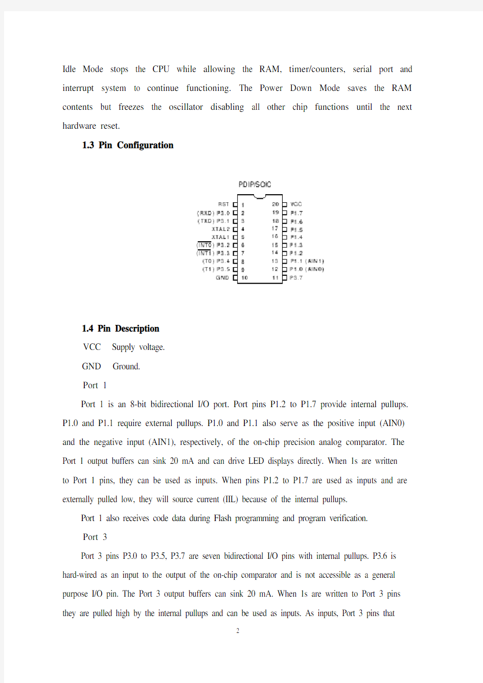
1.3 Pin Configuration
1.4 Pin Description
VCC Supply voltage.
GND Ground.
Port 1
Port 1 is an 8-bit bidirectional I/O port. Port pins P1.2 to P1.7 provide internal pullups. P1.0 and P1.1 require external pullups. P1.0 and P1.1 also serve as the positive input (AIN0) and the negative input (AIN1), respectively, of the on-chip precision analog comparator. The Port 1 output buffers can sink 20 mA and can drive LED displays directly. When 1s are written to Port 1 pins, they can be used as inputs. When pins P1.2 to P1.7 are used as inputs and are externally pulled low, they will source current (IIL) because of the internal pullups.
Port 1 also receives code data during Flash programming and program verification.
Port 3
Port 3 pins P3.0 to P3.5, P3.7 are seven bidirectional I/O pins with internal pullups. P3.6 is hard-wired as an input to the output of the on-chip comparator and is not accessible as a general purpose I/O pin. The Port 3 output buffers can sink 20 mA. When 1s are written to Port 3 pins they are pulled high by the internal pullups and can be used as inputs. As inputs, Port 3 pins that
are externally being pulled low will source current (IIL) because of the pullups.
Port Alternate Functions
P3.0 RXD (serial input port)
P3.1 TXD (serial output port)
P3.2 INT0 (external interrupt 0)
P3.3 INT1 (external interrupt 1)
P3.4 T0 (timer 0 external input)
P3.5 T1 (timer 1 external input)
Port 3 also serves the functions of various special features of the A T89C2051 as listed below:
1.5 Oscillator Characteristics
XTAL1 and XTAL2 are the input and output, respectively, of an inverting amplifier which can be configured for use as an on-chip oscillator, as shown in Figure 1. Either a quartz crystal or ceramic resonator may be used. To drive the device from an external clock source, XTAL2 should be left unconnected while XTAL1 is driven as shown in Figure 2. There are no re-quirements on the duty cycle of the external clock signal, since the input to the internal clocking circuitry is through a divideby-two flip-flop, but minimum and maximum voltage high and low time specifications must be observed.
1.6 Special Function Registers
A map of the on-chip memory area called the Special Function Register (SFR) space is shown in the table below.
Note that not all of the addresses are occupied, and unoccupied addresses may not be implemented on the chip. Read accesses. to these addresses will in general return random data, and write accesses will have an indeterminate effect.
User software should not write 1s to these unlisted locations, since they may be used in future products to invoke new fea tures. In that case, the reset or inactive values of the new bits will always be 0.
1.7 Restrictions on Certain Instructions
The AT89C2051 and is an economical and cost-effective mem ber of Atmel’s growing
family of microcontrollers. It contains 2 Kbytes of flash program memory. It is fully compatible with the MCS-51 architecture, and can be programmed using the MCS-51 instruction set. However, there are a few considerations one must keep in mind when utilizing certain instructions to program this device.
All the instructions related to jumping or branching should be restricted such that the destination address falls within the physical program memory space of the device, which is 2K for the AT89C2051. This should be the responsibility of the software programmer. For example, LJMP 7E0H would be a valid instruction for the AT89C2051 (with 2K of memory), whereas LJMP 900H would not.
1. Branching instructions:
LCALL, LJMP, ACALL, AJMP, SJMP, JMP @A+DPTR
These unconditional branching instructions will execute correctly as long as the programmer keeps in mind that the destination branching address must fall within the physical boundaries of the program memory size (locations 00H to 7FFH for the 89C2051). Violating the physical space limits may cause unknown program behavior.
CJNE [...], DJNZ [...], JB, JNB, JC, JNC, JBC, JZ, JNZ With these conditional branching instructions the same rule above applies. Again, violating the memory boundaries may cause erratic execution.
For applications involving interrupts the normal interrupt service routine address locations of the 80C51 family architecture have been preserved.
2. MOVX-related instructions, Data Memory:
The A T89C2051 contains 128 bytes of internal data memory. Thus, in the A T89C2051 the stack depth is limited to 128 bytes, the amount of available RAM. External DA TA memory access is not supported in this device, nor is external PROGRAM memory execution. Therefore, no MOVX [...] instructions should be included in the program.
A typical 80C51 assembler will still assemble instructions, even if they are written in violation of the restrictions mentioned above. It is the responsibility of the controller user to know the physical features and limitations of the device being used and adjust the instructions used correspondingly.
1.8 Program Memory Lock Bits
On the chip are two lock bits which can be left unprogrammed (U) or can be programmed (P) to obtain the additional features listed in the table below:
Lock Bit Protection Modes(1)
Program Lock Bits
LB1 LB2 Protection Type
1 U U No program lock features.
2 P U Further programming of the Flash is disabled.
3 P P Same as mode 2, also verify is disabled.
Note: 1. The Lock Bits can only be erased with the Chip Erase operation
1.9 Idle Mode
In idle mode, the CPU puts itself to sleep while all the on-chip peripherals remain active. The mode is invoked by software. The content of the on-chip RAM and all the special functions registers remain unchanged during this mode. The idle mode can be terminated by any enabled interrupt or by a hardware reset.
P1.0 and P1.1 should be set to ’0’ if no external pullups are used, or set to ’1’ if external pullups are used.
It should be noted that when idle is terminated by a hardware reset, the device normally resumes program execution, from where it left off, up to two machine cycles before the internal reset algorithm takes control. On-chip hardware inhibits access to internal RAM in this event, but access to the port pins is not inhibited. To eliminate the possibility of an unexpected write to a port pin when Idle is terminated by reset, the instruction following the one that invokes Idle should not be one that writes to a port pin or to external memory.
1.10 Power Down Mode
In the power down mode the oscillator is stopped, and the instruction that invokes power down is the last instruction executed. The on-chip RAM and Special Function Registers retain their values until the power down mode is terminated. The only exit from power down is a
hardware reset. Reset redefines the SFRs but does not change the on-chip RAM. The reset should not be activated before VCC is restored to its normal operating level and must be held active long enough to allow the oscillator to restart and stabilize.
P1.0 and P1.1 should be set to ’0’ if no external pullups are used, or set to ’1’ if external pullups are used.
1.11 Programming The Flash
The A T89C2051 is shipped with the 2 Kbytes of on-chip PEROM code memory array in the erased state (i.e., contents = FFH) and ready to be programmed. The code memory array is programmed one byte at a time. Once the array is programmed, to re-program any non-blank byte, the entire memory array needs to be erased electrically.
Internal Address Counter: The A T89C2051 contains an internal PEROM address counter which is always reset to 000H on the rising edge of RST and is advanced by applying a positive going pulse to pin XTAL1.
Programming Algorithm: To program the A T89C2051, the following sequence is recommended.
1. Power-up sequence:
Apply power between VCC and GND pins Set RST and XTAL1 to GND
With all other pins floating, wait for greater than 10 milliseconds
2. Set pin RST to ’H’ Set pin P
3.2 to ’H’
3. Apply the appropriate combination of ’H’ or ’L’ logic leve ls to pins P3.3, P3.4, P3.5, P3.7 to select one of the programming operations shown in the PEROM Programming Modes table.
To Program and V erify the Array:
4. Apply data for Code byte at location 000H to P1.0 to P1.7.
5. Raise RST to 12V to enable programming.
6. Pulse P3.2 once to program a byte in the PEROM array or the lock bits. The byte-write cycle is self-timed and typically takes 1.2 ms.
7. To verify the programmed data, lower RST from 12V to logic ’H’ level and set pins P3.3 to P3.7 to the appropiate levels. Output data can be read at the port P1 pins.
8. To program a byte at the next address location, pulse XTAL1 pin once to advance the
internal address counter. Apply new data to the port P1 pins.
9. Repeat steps 5 through 8, changing data and advancing the address counter for the entire 2 Kbytes array or until the end of the object file is reached.
10. Power-off sequence: set XTAL1 to ’L’ set RST to ’L’
Float all other I/O pins Turn Vcc power off
Data Polling: The AT89C2051 features Data Polling to indicate the end of a write cycle. During a write cycle, an attempted read of the last byte written will result in the complement of the written data on P1.7. Once the write cycle has been completed, true data is valid on all outputs, and the next cycle may begin. Data Polling may begin any time after a write cycle has been initiated.
Ready/Busy: The Progress of byte programming can also be monitored by the RDY/BSY output signal. Pin P3.1 is pulled low after P3.2 goes High during programming to indicate BUSY. P3.1 is pulled High again when programming is done to indicate READY.
Program Verify: If lock bits LB1 and LB2 have not been programmed code data can be read back via the data lines for verification:
1. Reset the internal address counter to 000H by bringing RST from ’L’ to ’H’.
2. Apply the appropriate control signals for Read Code data and read the output data at the port P1 pins.
3. Pulse pin XTAL1 once to advance the internal address counter.
4. Read the next code data byte at the port P1 pins.
5. Repeat steps 3 and 4 until the entire array is read.
The lock bits cannot be verified directly. V erification of the lock bits is achieved by observing that their features are enabled.
Chip Erase: The entire PEROM array (2 Kbytes) and the two Lock Bits are erased electrically by using the proper combination of control signals and by holding P3.2 low for 10 ms. The code array is written with all "1"s in the Chip Erase operation and must be executed before any non-blank memory byte can be re-programmed.
Reading the Signature Bytes: The signature bytes are read by the same procedure as a normal verification of locations 000H, 001H, and 002H, except that P3.5 and P3.7 must be pulled to a logic low. The values returned are as follows.
(000H) = 1EH indicates manufactured by Atmel (001H) = 21H indicates 89C2051
Programming Interface
Every code byte in the Flash array can be written and the entire array can be erased by using the appropriate combination of control signals. The write operation cycle is self-timed and once initiated, will automatically time itself to completion.
All major programming vendors offer worldwide support for the Atmel microcontroller series. Please contact your local programming vendor for the appropriate software revision.
Ultrasonic ranging system design
Publication title: Sensor Review. Bradford: 1993. Vol.
ABSTRACT:Ultrasonic ranging technology has wide using worth in many fields,such as the industrial locale,vehicle navigation and sonar engineering.Now it has been used in level measurement,self-guided autonomous vehicles, fieldwork robots automotive navigation,air and underwater target detection,identification,location and so on.So there is an important practicing meaning to learn the ranging theory and ways deeply. To improve the precision of the ultrasonic ranging system in hand,satisfy the request of the engineering personnel for the ranging precision,the bound and the usage,a portable ultrasonic ranging system based on the single chip processor was developed.
Keywords:Ultrasound r,Ranging System,Single Chip Processor
1.Introductive
With the development of science and technology, the improvement of people's standard of living, speeding up the development and construction of the city. urban drainage system have greatly developed their situation is constantly improving. However, due to historical reasons many unpredictable factors in the synthesis of her time, the city drainage system. In particular drainage system often lags behind urban construction. Therefore, there are often good building excavation has been building facilities to upgrade the drainage system phenomenon. It brought to the city sewage, and it is clear to the city sewage and drainage culvert in the sewage treatment system. comfort is very important to people's lives. Mobile robots designed to clear the drainage culvert and the automatic control system Free sewage culvert clear guarantee robot, the robot is designed to clear the culvert sewage to the core. Control System is the core component of the development of ultrasonic range finder. Therefore, it is very important to design a good ultrasonic range finder.
2. A principle of ultrasonic distance measurement
2.1 The principle of piezoelectric ultrasonic generator
Piezoelectric ultrasonic generator is the use of piezoelectric crystal resonators to work. Ultrasonic generator, the internal structure as shown, it has two piezoelectric chip and a resonance plate. When it's two plus pulse signal, the frequency equal to the intrinsic piezoelectric oscillation frequency chip, the chip will happen piezoelectric resonance, and promote the development of plate vibration resonance, ultrasound is generated. Conversely, if the two are not inter-electrode voltage, when the board received ultrasonic resonance, it will be for vibration suppression of piezoelectric chip, the mechanical energy is converted to electrical signals, then it becomes the ultrasonic receiver.
The traditional way to determine the moment of the echo's arrival is based on thresholding the received signal with a fixed reference. The threshold is chosen well above the noise level, whereas the moment of arrival of an echo is defined as the first moment the echo signal surpasses that threshold. The intensity of an echo reflecting from an object strongly depends on the object's nature, size and distance from the sensor. Further, the time interval from the echo's starting point to the moment when it surpasses the threshold changes with the intensity of the echo. As a consequence, a considerable error may occur Even two echoes with different intensities arriving exactly at the same time will surpass the threshold at different moments. The stronger one will surpass the threshold earlier than the weaker, so it will be considered as belonging to a nearer object.
2.2The principle of ultrasonic distance measurement
Ultrasonic transmitter in a direction to launch ultrasound, in the moment to launch the beginning of time at the same time, the spread of ultrasound in the air, obstacles on his way to return immediately, the ultrasonic reflected wave received by the receiver immediately stop the clock. Ultrasound in the air as the propagation velocity of 340m / s, according to the timer records the time t, we can calculate the distance between the launch distance barrier (s), that is: s = 340t / 2
3.Ultrasonic Ranging System for the Second Circuit Design
System is characterized by single-chip microcomputer to control the use of ultrasonic transmitter and ultrasonic receiver since the launch from time to time, single-chip selection of 8751, economic-to-use, and the chip has 4K of ROM, to facilitate programming. Circuit schematic diagram shown in Figure 2.
Figure 1 circuit principle diagram
3.1 40 kHz ultrasonic pulse generated with the launch
Ranging system using the ultrasonic sensor of piezoelectric ceramic sensors UCM40, its operating voltage of the pulse signal is 40kHz, which by the single-chip implementation of the following procedures to generate.
puzel: mov 14h, # 12h; ultrasonic firing continued 200ms
here: cpl p1.0; output 40kHz square wave
Ranging in front of single-chip termination circuit P1.0 input port, single chip implementation of the above procedure, the P1.0 port in a 40kHz pulse output signal, after amplification transistor T, the drive to launch the first ultrasonic UCM40T, issued 40kHz ultrasonic pulse, and the continued launch of 200ms. Ranging the right and the left side of the circuit, respectively, then input port P1.1 and P1.2, the working principle and circuit in front of the same location.
3.2 Reception and processing of ultrasonic
Used to receive the first launch of the first pair UCM40R, the ultrasonic pulse modulation signal into an alternating voltage, the op-amp amplification IC1A and after polarization IC1B to IC2. IC2 is locked loop with audio decoder chip LM567, internal voltage-controlled oscillator center frequency of f0 = 1/1.1R8C3, capacitor C4 determine their target bandwidth. R8-conditioning in the launch of the carrier frequency on the LM567 input signal is greater than 25mV, the output from the high jump 8 feet into a low-level, as interrupt request signals to the single-chip processing.
Ranging in front of single-chip termination circuit output port INT0 interrupt the highest priority, right or left location of the output circuit with output gate IC3A access INT1 port single-chip, while single-chip P1.3 and P1. 4 received input IC3A, interrupted by the process to identify the source of inquiry to deal with, interrupt priority level for the first left right after. Part of the source code is as follows:
receive1: push psw
push acc
clr ex1; related external interrupt 1
jnb p1.1, right; P1.1 pin to 0, ranging from right to interrupt service routine circuit
jnb p1.2, left; P1.2 pin to 0, to the left ranging circuit interrupt service routine
return: SETB EX1; open external interrupt 1
pop acc
pop psw
reti
right: ...; right location entrance circuit interrupt service routine
Ajmp Return
left: ...; left Ranging entrance circuit interrupt service routine
Ajmp Return
3.3 The calculation of ultrasonic propagation time
When you start firing at the same time start the single-chip circuitry within the timer T0, the use of timer counting function records the time and the launch of ultrasonic reflected wave received time. When you receive the ultrasonic reflected wave, the receiver circuit outputs a negative jump in the end of INT0 or INT1 interrupt request generates a signal, single-chip microcomputer in response to external interrupt request, the implementation of the external interrupt service subroutine, read the time difference, calculating the distance . Some of its source code is as follows:
RECEIVE0: PUSH PSW
PUSH ACC
CLR EX0; related external interrupt 0
MOV R7, TH0; read the time value
MOV R6, TL0
CLR C
MOV A, R6
SUBB A, # 0BBH; calculate the time difference
MOV 31H, A; storage results
MOV A, R7
SUBB A, # 3CH
MOV 30H, A
SETB EX0; open external interrupt 0
POP ACC
POP PSW
RETI
For a flat target, a distance measurement consists of two phases: a coarse measurement and. a fine measurement:
Step 1: Transmission of one pulse train to produce a simple ultrasonic wave.
Step 2: Changing the gain of both echo amplifiers according to equation , until the echo is detected.
Step 3: Detection of the amplitudes and zero-crossing times of both echoes.
Step 4: Setting the gains of both echo amplifiers to normalize the output at, say 3 volts. Setting the period of the next pulses according to the : period of echoes. Setting the time window according to the data of step 2.
Step 5: Sending two pulse trains to produce an interfered wave. Testing the zero-crossing times and amplitudes of the echoes. If phase inversion occurs in the echo, determine to otherwise calculate to by interpolation using the amplitudes near the trough. Derive t sub m1 and t sub m2 .
Step 6: Calculation of the distance y using equation .
4. The ultrasonic ranging system software design
Software is divided into two parts, the main program and interrupt service routine. Completion of the work of the main program is initialized, each sequence of ultrasonic transmitting and receiving control.
Interrupt service routines from time to time to complete three of the rotation direction of ultrasonic launch, the main external interrupt service subroutine to read the value of completion time, distance calculation, the results of the output and so on.
5. Conclusions
Required measuring range of 30cm ~ 200cm objects inside the plane to do a number of measurements found that the maximum error is 0.5cm, and good reproducibility.
Single-chip design can be seen on the ultrasonic ranging system has a hardware structure is simple, reliable, small features such as measurement error. Therefore, it can be used not only for mobile robot can be used in other detection systems.
Thoughts: As for why the receiver do not have the transistor amplifier circuit, because the magnification well, integrated amplifier, but also with automatic gain control level, magnification to 76dB, the center frequency is 38k to 40k, is exactly resonant ultrasonic sensors frequency.
AT89C2051微控制器的指令
一、特点
?兼容MCS - 51产品
?2个字节的可再编程闪存
耐力擦写/擦除周期
?2. 7 V至6 V工作范围
?全静态操作0 Hz至24 MHz的
?两级程序存储器锁定
?128 ×8位内部RAM
?15个可编程I / O线
?2个16位定时器/计数器
?六个中断源
?可编程串行UART通道
?直接LED驱动输出
?片上模拟比较器
?低功耗空闲和掉电模式
二、说明
该AT89C2051是一个低电压,高性能CMOS 8位2 Kby ?的Flash可编程,可擦除只读存储器(PEROM)设备是制造? tured采用Atmel的高密度非易失性内存技术,并与兼容的工商业污水附加费微机工业标准MCS - 51指令集,并通过结合在一个通用的单芯片闪存的8位CPU引脚,Atmel的AT89C2051是一种功能强大的微机提供了高度灵活和成本效益的解决方案,许多嵌入式控制应用
该AT89C2051提供以下标准功能2字节的闪存,128字节RAM,15 I / O线,两个16位定时器/计数器,一个五向量2级中断结构,一个全双工串行口,一个精密模拟比较器,片上振荡器和时钟电路此外,该AT89C2051的设计与操作频率下降到零静态逻辑,支持两种软件可选的节电模式空闲模式时CPU停止工作,同时允许RAM,定时/计数器,串行口和中断系统继续工作暂停模式保存RAM的内容,但冻结,直到下一个硬件复位振荡器禁用所有其他芯片功能
三、引脚配置
四、引脚说明
VCC电源电压
GND接地
端口1
端口1是一个8位双向I / O端口端口引脚P1 2至7提供P1 P1和P1 0 1 0内部上拉需要P1和P1 1外部上拉也可作为正输入(AIN0)和负输入(AIN1 ),分别对片内精密模拟比较器的端口1输出缓冲器可以吸收20mA的电流,并且可以直接驱动LED时1秒写入端口1引脚,它们可以作为输入引脚P1 2时至P17顷作为输入,并从外部拉低,将输出电流(IIL)由于内部上拉在端口1也接收片内Flash存储。
端口3
P3口P3 0至5 P3,P37顷带有内部上拉P3 6 seven双向I / O引脚是作为对片上比较器输出输入硬连接,而不是作为一个通用访问?构成我/ O引脚的3口输出缓冲器可吸收20mA当1秒写入端口3他们拉高内部上拉,可作为作为输入,3口被外部拉低的引脚为低电平输入的引脚将输出电流(IIL)由于上拉在端口3也接收片内Flash存储。
端口引脚的第二功能
P3 0 RXD(串行输入口)
P3 1 TXD(串行输出端口)
P3 2 INT0(外部中断0)
P3 3 INT1(外部中断1)
P3 4 T0(定时器0外部输入)
端口3也可以用下面列出的AT89C2051各种特殊功能,
五、振荡器特性
XTAL1和XTAL2分别是输入和输出,分别为一个反相放大器,可用于作为一个片上振荡器使用配置,如图1无论是石英晶体或陶瓷谐振器可用于驱动外部显示设备时钟源,XTAL2应悬空而XTAL1驱动,如图2所示有没有重新?quirements 对外部时钟信号的占空比,由于内部时钟电路的输入通过鸿沟?由二翻转翻牌,但最小和最大电压高和低时间规范必须遵守。
六、特殊功能寄存器
一个片上内存区域的地图称为特殊功能寄存器(SFR)空间中的表所示请注意,并非所有的地址都被占用,并无人居住地址可能无法在芯片上实现的读取访问这些地址。
七、某些指令的限制
该AT89C2051是一种经济和成本效益的纪念品,Atmel的越来越多的微控制器系列。
BER它包含2闪存程序存储器,是完全与MCS - 51架构兼容,并能进行编程使用。MCS - 51指令集然而,也有少数的审议?操作之一时,必须牢记某些指令计划利用此装置有关的所有分支指令跳跃或应限制在物理方案的设备,这是2K的AT89C2051。
这应该是软的责任?软件例如程序员的内存空间,这样的目标地址瀑布,LJMP 7E0H会是为AT89C2051(2K的内存)有效指令,而LJMP 900H不会1分支指令。
LCALL,LJMP,ACALL,AJMP,SJMP,JMP @ A + DPTR
这些无条件分支指令将执行心病?rectly只要记住保持程序员的目的地?TION 分支。
地址必须在程序存储器的大小(位置为00H的89C2051 7FFH)的物理边界下降违反物理空间限制可能导致联合国?已知程序的行为。
CJNE [],DJNZ [],JB,JNB,JC,JNC,JBC,JZ,JNZ有了这些条件分支指令上述AP ?层数相同的规则同样,侵犯边界的内存可能会导致二? ratic执行。
对于涉及中断应用的正常中断SERV ?冰例行的80C51系列架构地址位置已被保存。
2 MOVX相关指令,数据存储器
该AT89C2051包含128字节的内部数据存储器因此,在AT89C2051的堆栈深度限制为128字节,可用RAM外部数据存储器访问量是不支持这个设备,也不是外部程序存储器执行,因此,没有MOVX [ ]说明应包括在该计划。
一个典型的80C51汇编器将仍然组装说明,即使是在它上面提到的限制是违反书面控制器的用户有责任了解的物理特性和所使用的设备限制,并调整相应的使用说明。
八、程序存储器锁定位
在芯片上有两个锁,可以不编程(U),也可以编程(P)位获得该表中列出以下的附加功能。
九、空闲模式
在空闲模式下,CPU进入睡眠状态,而所有片上外设仍然有效的模式是通过软件调用的片上RAM的内容,包括所有的特殊功能寄存器保持不变,在此模式空闲模式可以被终止任何使能的中断或硬件复位。
P1 0和P1 1应设置为0,如果没有外部上拉电阻的使用,或设置为'1',如果使用外部上拉,应该指出的是,空闲时被硬件复位终止,恢复设备正常程序执行,从那里离开的,最多两个机器周期之前,内部复位算法需要控制片上硬件抑制这种访问内部RAM事件,但访问端口引脚是不禁止为了消除意想不到的可能性,写一个端口引脚空闲时被复位终止,指令FOL ? lowing一个调用不应该是一个空闲写入到端口引脚或外部存储器。
十、掉电模式
在掉电模式,振荡器停止,并在?结构形式的调用断电是最后一个指令EXE ?cuted片上RAM和特殊功能寄存器的值保持不变,直到掉电模式终止从电源唯一的出口下一个硬件复位复位重新定义了SFR,但不改变片上RAM的复位不应该被启动才能VCC恢复到正常工作的水平,必须持有足够长的活跃,使振荡器重新启动并稳定P1 0和P1 1应设置为0,如果没有外部上拉电阻的使用,或设置为'1',也可以使用外部上拉。
十一、Flash进行编程
该AT89C2051是随片上PEROM代码存储阵列的2千字节的擦除状态(即,内
容= FFH),并准备进行编程代码存储器阵列的编程以一次一个字节数组一旦被编程,以重新编程的任何非空白字节,整个存储器阵列需要电擦除内部地址计数器的。
AT89C2051包含一个?ternal PEROM地址计数器它总是在RST复位的上升沿000H,并通过应用了正脉冲引脚XTAL1先进规划算法程序的AT89C2051,按下列顺序推荐。
电序列,应用在VCC和GND引脚发电机组RST和XTAL1和GND与所有其他引脚浮动,等待大于10毫秒。
SET引脚RST为“H”SET引脚P3 2“H”。
申请的“H”或“L”适当的组合逻辑电平的引脚3 P3,P3 4,5 P3,P3 7选择亲one ?编程作业在PEROM编程模式表所示编程和验证阵列。
应用在位置000H到P1 P1 7 5 0字节数据的代码RST提高到12V,使编程6脉冲P3 2一次计划在PEROM阵列或锁定位字节的字节写周期是自定时的典型? cally 需要1 2毫秒。
要核实编程的数据,降低RST从12V到逻辑“H”级,并设置3至P3 P3引脚7到适当的水平输出的数据可以读取的P1口引脚。
要程序中的下一个地址字节的位置,脉冲XTAL1脚一次推进内部地址计数器将新数据到P1口引脚。
重复步骤5到8,更改数据,并推动整个2千字节数组的地址计数器或直至达到最终目标文件。
断电序列设置XTAL1为“L”设置RST为“L”浮法所有其他I / O引脚切断VCC
数据轮询AT89C2051功能数据轮询悠?美食一个写周期期间写周期结束时,企图形最后写入的字节读将在7 P1上写入数据的补充结果一旦写周期已经完成,真正的数据是对所有输出有效,下一个周期可能开始数据轮询可能会开始后的任何时间写周期已启动就绪/忙字节编程的进展,也可以由RDY / BSY输出信号引脚P3 P3后拉1 2低监控云在编程过程中,以指示BUSY P3 1被拉高时再进行编程,以指示READY高程序验证如果锁定位LB1和LB2没有亲?编程代码数据可以回读通过的veri ? fication数据线。
1复位内部地址计数器000H通过把“L”RST为“H”
2申请读代码数据相应的控制信号,并在读P1口引脚的输出数据
3脉冲引脚XTAL1一次推进内部地址计数器
4阅读的P1口引脚5重复步骤3和4的下一个代码数据字节,直到整个数组读锁定位不能直接验证的锁位验证是通过观察他们的特点是启用芯片擦除整个PEROM阵列(2字节)和两个锁定位的电擦除通过使用适当的控制信号组合? TION 和持有10毫秒代码阵列P3 2低是全“1”,在的书面芯片擦除操作之前,必须执行任何非空存储字节可重新编程读标识字节的签名字节是由一个地点000H,001H和002H正常核查的程序相同,只是读5 P3和P3 7,必须拉至低的值返回的逻辑如下。
(000H)= 1EH表示由Atmel公司(001H)= 21H表示制造89C2051
编程接口
闪存阵列中的每个字节代码可以写入和可擦除整个阵列使用适当的浓度控制信号的组合?写操作周期是自定时的,一旦?itiated,时间本身将自动完成所有主要的编程供应商提供的爱特梅尔微控制器系列的全球支持,请联系相应的软件修改您的当地亲?编程供应商
外文文献: Knowledge of the stepper motor What is a stepper motor: Stepper motor is a kind of electrical pulses into angular displacement of the implementing agency. Popular little lesson: When the driver receives a step pulse signal, it will drive a stepper motor to set the direction of rotation at a fixed angle (and the step angle). You can control the number of pulses to control the angular displacement, so as to achieve accurate positioning purposes; the same time you can control the pulse frequency to control the motor rotation speed and acceleration, to achieve speed control purposes. What kinds of stepper motor sub-: In three stepper motors: permanent magnet (PM), reactive (VR) and hybrid (HB) permanent magnet stepper usually two-phase, torque, and smaller, step angle of 7.5 degrees or the general 15 degrees; reaction step is generally three-phase, can achieve high torque output, step angle of 1.5 degrees is generally, but the noise and vibration are large. 80 countries in Europe and America have been eliminated; hybrid stepper is a mix of permanent magnet and reactive advantages. It consists of two phases and the five-phase: two-phase step angle of 1.8 degrees while the general five-phase step angle of 0.72 degrees generally. The most widely used Stepper Motor. What is to keep the torque (HOLDING TORQUE) How much precision stepper motor? Whether the cumulative: The general accuracy of the stepper motor step angle of 3-5%, and not cumulative.
会计内部控制中英文对照外文翻译文献(文档含英文原文和中文翻译)
内部控制透视:理论与概念 摘要:内部控制是会计程序或控制系统,旨在促进效率或保证一个执行政策或保护资产或避免欺诈和错误。内部是一个组织管理的重要组成部分。它包括计划、方法和程序使用,以满足任务,目标和目的,并在这样做,支持基于业绩的管理。内部控制是管理阶层的平等与控制可以帮助管理者实现资源的预期的有效管理的结果通过。内部控制应减少或违规错误的风险关联未被发现的,但设计和建立有效的内部控制不是一个简单的任务,不可能是一个实现通过快速修复短套。在此讨论了内部文件的概念的不同方面的内部控制和管制。 关键词:内部控制,管理控制,控制环境,控制活动,监督 1、介绍 环境需要新的业务控制变量不为任何潜在的股东和管理人士的响应因子为1,另外应执行/她组织了一个很大的控制权。控制是管理活动的东西或以上施加控制。思想的产生和近十年的发展需要有系统的商业资源和控制这种财富一个新的关注。主题之一热一回合管制的商业资源是分析每个控制成本效益。 作为内部控制和欺诈的第一道防线,维护资产以及预防和侦查错误。内部控制,我们可以说是一种控制整个系统的财务和其他方面的管理制定了为企业的顺利运行;它包括内部的脸颊,内部审计和其他形式的控制。 COSO的内部控制描述如下。内部控制是一个客观的方法用来帮助确保实现。在会计和组织理论,内部控制是指或目标目标的过程实施由组织的结构,工作和权力流动,人员和具体的管理信息系统,旨在帮助组织实现。这是一种手段,其中一个组织的资源被定向,监控和测量。它发挥着无形的(重要的作用,预防和侦查欺诈和保护组织的资源,包括生理(如,机械和财产)和乙二醇,声誉或知识产权,如商标)。在组织水平,内部控制目标与可靠性的目标或战略的财务报告,及时反馈业务上的成就,并遵守法律,法规。在具体的交易水平,内部控制是指第三方采取行动以实现一个具体目标(例如,如何确保本组织的款项,在申请服务提供有效的。)内部控制程序reduce程变异,导
杭州电子科技大学信息工程学院毕业设计(论文)外文文献翻译 毕业设计(论文)题目用单片机实现的数字时钟电路设计文献综述题目单片机控制系统系电子工程 专业电子信息科学与技术 姓名郭筱楠 班级08091911 学号08919115 指导教师王维平
单片机控制系统 广义地说,微型计算机控制系统(单片机控制系统)是用于处理信息的,这种被用于处理的信息可以是电话交谈,也可以是仪器的读数或者是一个企业的帐户,但是各种情况下都涉及到相同的主要操作:信息的处理、信息的存储和信息的传递。在常规的电子设计中,这些操作都是以功能平台方式组合起来的,例如计数器,无论是电子计数器还是机械计数器,都要存储当前的数值,并且按要求将该数值增加1。一个系统例如采用计数器的电子钟之类的任一系统要使其存储和处理能力遍布整个系统,因为每个计数器都能存储和处理一些数字。 现如今,以微处理器为基础的系统从常规的处理方法中分离了出来,它将信息的处理,信息的存储和信息的传输三个功能分离形成不同的系统单元。这种主要将系统分成三个主要单元的分离方法是冯-诺依曼在20世纪40年代所设想出来的,并且是针对微计算机的设想。从此以后基本上所有制成的计算机都是用这种结构设计的,尽管他们包含着宽广的物理形式与物理结构,但从根本上来说他们均是具有相同基本设计的计算机。 在以微处理器为基础的系统中,处理是由以微处理器为基础的系统自身完成的。存储是利用存储器电路,而从系统中输入和输出的信息传输则是利用特定的输入/输出(I/O)电路。要在一个以微处理器为基础的时钟中找出执行具有计数功能的一个特殊的硬件组成部分是不可能的,因为时间存储在存储器中,而在固定的时间间隔下由微处理器控制增值。但是,规定系统运转过程的软件却规定了包含实现计数器计数功能的单元部分。由于系统几乎完全由软件所定义,所以对微处理器结构和其辅助电路这种看起来非常抽象的处理方法使其在应用时非常灵活。这种设计过程主要是软件工程,而且在生产软件时,就会遇到产生于常规工程中相似的构造和维护问题。 图1.1 微型计算机的三个组成部分 图1.1显示出了微型计算机中这三个单元在一个微处理器控制系统中是如何按照机器中的信息通信方式而联接起来的。该系统由微处理器控制,微处理器能够对其自身的存储器和输入/输出单元的信息传输进行管理。外部的连接部分与
附录A
附录B 如何监测内部控制 内部控制是任何组织有效运行的关键,董事会、执行长和内部审计人员都为实现这个企业的目标而工作;该内部控制系统是使这些团体确保那些目标的达成的一种手段。控制帮助一个企业有效率地运转。此外,运用一种有效的风险系统,风险可被降低到最小。同时,控制促进经营和与经营有关的信息的可靠性。全美反舞弊性财务报告委员会发起组织(COSO;1992) 在它发布的具有开创性的文件《内部控制整合框架》中,将内部控制定义为:企业风险管理是一个过程,受企业董事会、管理层和其他员工的影响,包括内部控制及其在战略和整个公司的应用,旨在为实现经营的效率和效果、财务报告的可靠性以及法规的遵循提供合理保证。该委员会还指出,一个的内部控制的系统包括五个要素。它们是:控制环境、风险评估、信息和沟通、控制活动、监控。 COSO的定义及五个要素已被证明确实对不同的团体,如董事会和首席执行官起到作用。这些群体对内部控制系统的监管以及系统设计与运行有责任。而且,内部审计人员已经发现COSO的指导是有用的。这群人员可能会被董事会或管理层要求去测试控制。COSO最近发布的一份讨论文件,指出五个要素监控,其中的五个要素的确定在1992 frame work COSO原本。中国发展简报的题为《内部控制-整合框架:内部控制体系监督指南》(COSO,2007)。在文件中,COSO 强调监控的重要性,以及这些信息常常被没有充分利用。 因为董事会、执行长,和内部审计人员都在一个公司的内部控制中扮演着重要角色,内部控制的各要素,包括监测,都对所有的团体有着非常重要的意义。同时,外审计人员对监测有兴趣。《萨班斯-奥克斯利法案》(2002)为外部审计师创建了一个新的监督体制。所有的五个要素,包括监测,必须加以考虑。另外,内部控制审计必须结合对财务报告的检查。在一体化审计之前,在首席执行官的领导下,也许也在内部审计活动的支持下的管理,评估了内控制体系的有效性。随后外部审计人员对控制出具意见。起监督角色的董事会,将阅读内部审计、管理层和首席执行官出具的报告。文件关于监测对每一个团体的指导起了帮助,因为他们分别为各自的角色而劳动。 第一,什么是监测。监测的组成可评估内部控制系统在过去一段时间发挥效用的质量。其对控制功能的评估有助于企业确定其控制在有效地运作中。在执行监测活动时,相关人员参与审查系统的设计及其运行效果。这种检查必须进行及时,目的是为了提供给企业最大的利益。管理层负责做出适当的行动以回应这些结果。当事人对内部控制有兴趣,可以充分依赖这个内部控制系统,如果合适的监
外文文献一单片机简介 单片机是一种集成在电路芯片,是采用超大规模集成电路技术把具有数据处理能力的中央处理器CPU随机存储器RAM、只读存储器ROM、多种I/O口和中断系统、定时器/计时器等功能(可能还包括显示驱动电路、脉宽调制电路、模拟多路转换器、A/D转换器等电路)集成到一块硅片上构成的一个小而完善的计算机系统。单片机也被称为微控制器(Microcontroller),是因为它最早被用在工业控制领域。单片机由芯片内仅有CPU的专用处理器发展而来。最早的设计理念是通过将大量外围设备和CPU集成在一个芯片中,使计算机系统更小,更容易集成进复杂的而对体积要求严格的控制设备当中。INTEL的Z80是最早按照这种思想设计出的处理器,从此以后,单片机和专用处理器的发展便分道扬镳。 二、单片机的发展趋势 现在可以说单片机是百花齐放,百家争鸣的时期,世界上各大芯片制造公司都推出了自己的单片机,从8位、16位到32位,数不胜数,应有尽有,有与主流C51系列兼容的,也有不兼容的,但它们各具特色,互成互补,为单片机的应用提供广阔的天地。 纵观单片机的发展过程,可以预示单片机的发展趋势,大致有: 1.低功耗CMOS MCS-51系列的8031推出时的功耗达630mW,而现在的单片机普遍都在100mW左右,随着对单片机功耗要求越来越低,现在的各个单片机制造商基本都采用了CMOS(互补金属氧化物半导体工艺)。象80C51就采用了HMOS(即高密度金属氧化物半导体工艺)和CHMOS(互补高密度金属氧化物半导体工艺)。CMOS虽然功耗较低,但由于其物理特征决定其工作速度不够高,而CHMOS则具备了高速和低功耗的特点,这些特征,更适合于在要求低功耗象电池供电的应用场合。所以这种工艺将是今后一段时期单片机发展的主要途径。 2.微型单片化 现在常规的单片机普遍都是将中央处理器(CPU)、随机存取数据存储(RAM)、只读程序存储器(ROM)、并行和串行通信接口,中断系统、定时电路、时钟电路集成在一块单一的芯片上,增强型的单片机集成了如A/D转换器、PMW(脉宽调制电路)、WDT(看门狗)、有些单片机将LCD(液晶)驱动电路都集成在单一的芯片上,这样 单片机包含的单元电路就更多,功能就越强大。甚至单片机厂商还可以根据用户的要求量身定做,制造出具有. 自己特色的单片机芯片。此外,现在的产品普遍要求体积小、重量轻,这就要求单片机除了功能强和功耗低外,还要求其体积要小。现在的许多单片机都具有多种封装形式,其中SMD(表面封装)越来越受欢迎,使得由单片机构成的系统正朝微型化方向发展。 3.主流与多品种共存 现在虽然单片机的品种繁多,各具特色,但仍以80C51为核心的单片机占主流,兼容其结构和指令系统的有PHILIPS公司的产品,ATMEL公司的产品和中国台湾
中小企业内部控制_外文参考文献 安徽工业大学毕业设计外文翻译 Private Enterprises of the intenal control issues Pulin Chang Economic Review. 2008, (5) Third, the promotion of private SMEs in the internal control system strategy (A) change management and business owners the concept of development. The majority of private small and medium enterprises in the family business, the success of these enterprises depends largely on internal control or entrepreneur leadership attention and level of implementation. Over the years, by traditional Chinese culture, business owners believe in Sincerity, fraternal loyalty permeate many aspects of enterprise management, strengthen internal controls that will affect the organization the members of distrust, resulting in internal control. Many private business owners that rely on business to do business benefits out of, rather than out of the internal financial management control; that the market is the most important internal control will be bound himself and staff development. Understanding of the bias, so that these leaders neglected the internal control system on the production and operation activities. Internal control can really become the leader of the internal needs of enterprise internal control system is the key to whether a mere formality. The internal control to make the internal needs of the enterprise depends largely on two points: First, determine
外文资料翻译 STC89C52 processi ng chip Prime features: With MCS - 51 SCM product compatibility, 8K bytes in the system programmable Flash memory, 1000 times CaXie cycle, the static operation: 0Hz ~ 33Hz, triple encryption program memory, 32 programmed I/O port, three 16 timer/counter, the eight uninterrupted dual-career UART serial passage, low power consumption, leisure and fall after fall electric power mode can be awakened and continuous watchdog timer and double-number poin ter, power ide ntifier. Efficacy: characteristics STC89C52 is one kind of low power consumption, high CMOS8 bit micro-co ntroller, 8K in system programmable Flash memory. Use high-de nsity nonv olatile storage tech no logy, and in dustrial 80C51 product in structi on and pin fully compatible. The Flash memory chips allows programs in the system, also suitable for programmable conventional programming. In a single chip, have clever 8 bits CPU and on li ne system programmable Flash, in crease STC89C52 for many embedded control system to provide high vigorous application and useful solutions. STC89C52 has following standard efficacy: 8k byte Flash RAM, 256 bytes, 32 I/O port, the watchdog timer, two, three pointer numerical 16 timer/counter, a 6 vector level 2 continuous structure, the serial port, working within crystals and horological circuit. In addition, 0Hz AT89S52 can drop to the static logic operation, support two software can choose power saving mode. Idle mode, the CPU to stop working, and allows the RAM, timer/c oun ters, serial, continu ous to work. Protectio n asa na patter n, RAM content is survival, vibrators frozen, SCM, until all the work under a continuous or hardware reset. 8-bit microcontrollers 8K bytes in the system programmable Flash AT89S52 devices. Mouth: P0 P0 mouth is a two-way ope n drain I/O. As export, each can drive eight TTL logic level. For P0 port to write "1", foot as the high impeda nee in put. When access to exter nal programs and nu merical memory, also known as
SCM is an integrated circuit chip, is the use of large scale integrated circuit technology to a data processing capability of CPU CPU random access memory RAM, read-only memory ROM, a variety of I / O port and interrupt system, timers / timer functions (which may also include display driver circuitry, pulse width modulation circuit, analog multiplexer, A / D converter circuit) integrated into a silicon constitute a small and complete computer systems. SCM is also known as micro-controller (Microcontroller), because it is the first to be used in industrial control. Only a single chip by the CPU chip developed from a dedicated processor. The first design is by a large number of peripherals and CPU on a chip in the computer system, smaller, more easily integrated into a complex and demanding on the volume control device which. The Z80 INTEL is the first designed in accordance with this idea processor, then on the development of microcontroller and dedicated processors will be parting ways. Are 8-bit microcontroller early or 4 bits. One of the most successful is the INTEL 8031, for a simple, reliable and good performance was a lot of praise. Then developed in 8031 out of MCS51 MCU Systems. SCM systems based on this system until now is still widely used. With the increased requirements of industrial control field, began a 16-bit microcontroller, but not ideal because the cost has not been very widely used. After 90 years with the great development of consumer electronics, microcontroller technology has been a huge increase. With INTEL i960 series, especially the later series of widely used ARM, 32-bit microcontroller quickly replace high-end 16-bit MCU status and enter the mainstream market. The traditional 8-bit microcontroller performance have been the rapid increase capacity increase compared to 80 the number of times. Currently, high-end 32-bit microcontroller clocked over 300MHz, the performance catching the mid-90s dedicated processor, while the average model prices fall to one U.S. dollar, the most high-end [1] model only 10 dollars. Modern SCM systems are no longer only in the development and use of bare metal environment, a large number of proprietary embedded operating system is widely used in the full range of SCM. The handheld computers and cell phones as the core processing of high-end microcontroller can even use a dedicated Windows and Linux operating systems. SCM is more suitable than the specific processor used in embedded systems, so it was up to the application. In fact the number of SCM is the world's largest computer. Modern human life used in almost every piece of electronic and mechanical products will be integrated single chip. Phone, telephone, calculator, home appliances, electronic toys, handheld computers and computer accessories such as a mouse with a 1-2 in both the Department of SCM. Personal computer will have a large number of SCM in the work. General car with more than 40 microcontroller, a complex industrial control systems may even hundreds of single chip at the same time work! SCM is not only far exceeds the number of PC and other computing the sum, or even more than the number of human beings. Single chip, also known as single-chip microcontroller, it is not complete a certain logic chips, but to a computer system integrated into a chip. Equivalent to a
沈阳工程学院毕业设计(论文) 外文文献 一单片机简介 单片机是一种集成在电路芯片,是采用超大规模集成电路技术把具有数据处理能力的中央处理器CPU随机存储器RAM、只读存储器ROM、多种I/O口和中断系统、定时器/计时器等功能(可能还包括显示驱动电路、脉宽调制电路、模拟多路转换器、A/D转换器等电路)集成到一块硅片上构成的一个小而完善的计算机系统。 单片机也被称为微控制器(Microcontroller),是因为它最早被用在工业控制领域。单片机由芯片内仅有CPU的专用处理器发展而来。最早的设计理念是通过将大量外围设备和CPU集成在一个芯片中,使计算机系统更小,更容易集成进复杂的而对体积要求严格的控制设备当中。INTEL的Z80是最早按照这种思想设计出的处理器,从此以后,单片机和专用处理器的发展便分道扬镳。 二、单片机的发展趋势 现在可以说单片机是百花齐放,百家争鸣的时期,世界上各大芯片制造公司都推出了自己的单片机,从8位、16位到32位,数不胜数,应有尽有,有与主流C51系列兼容的,也有不兼容的,但它们各具特色,互成互补,为单片机的应用提供广阔的天地。 纵观单片机的发展过程,可以预示单片机的发展趋势,大致有: 1.低功耗CMOS MCS-51系列的8031推出时的功耗达630mW,而现在的单片机普遍都在100mW左右,随着对单片机功耗要求越来越低,现在的各个单片机制造商基本都采用了CMOS(互补金属氧化物半导体工艺)。象80C51就采用了HMOS(即高密度金属氧化物半导体工艺)和CHMOS(互补高密度金属氧化物半导体工艺)。CMOS虽然功耗较低,但由于其物理特征决定其工作速度不够高,而CHMOS则具备了高速和低功耗的特点,这些特征,更适合于在要求低功耗象电池供电的应用场合。所以这种工艺将是今后一段时期单片机发展的主要途径。 2.微型单片化 现在常规的单片机普遍都是将中央处理器(CPU)、随机存取数据存储(RAM)、只读程序存储器(ROM)、并行和串行通信接口,中断系统、定时电路、时钟电路集成在一块单一的芯片上,增强型的单片机集成了如A/D转换器、PMW(脉宽调制电路)、WDT(看门狗)、有些单片机将LCD(液晶)驱动电路都集成在单一的芯片上,这样单片机包含的单元电路就更多,功能就越强大。甚至单片机厂商还可以根据用户的要求量身定做,制造出具有自己特色的单片机芯片。此外,现在的产品普遍要求体积小、重量轻,这就要求单片机除了功能强和功耗低外,还要求其体积要小。现在的许多单片机都具有多种封装形式,其中SMD(表面封装)越来越受欢迎,使得由单片机构成的系统正朝微型化方向发
中文5900字 本科毕业设计(论文) 外文参考文献译文及原文 学院 专业 年级班别 学号 学生姓名 指导教师 年月日
中小民营企业内部控制研究 Research on the Internal Control of Small and Medium-sized Private Enterprises 目录 摘要 (1) 1 选题背景 (2) 2内部控制理论的概述 (3) 2.1 内部控制的根本性质 (3) 2.2内部控制的责任 (3) 3 确保内部控制的充分性 (5) 4 先天的内部控制 (9) 5 结论 (11) Abstract (12) 1Background Topics (13) 2 Internal control theory outlined (15) 2.1 The Fundamental Nature Of Intaral Control (15) 2.2 Responsibillty For Internal Control (15) 3 Ensuring that the internal control adequacy (17) 4 Inherent limitations of internal control (22) 5 Conclusion (25)
摘要 内部控制这个概念已经不是一个新概念。这篇文章将研究每个公共部门财政经理和董事会成员应该了解的关于内部控制的内容。在分析了虚假的财政报告的根本原因以后,Treadway 委员会把大部分的责任归咎于内部控制管理的不足。作为回应,建立Treadway委员会的各个组织成立了一个赞助组织委员会(COSO),设法补救的Treadway委员会揭露出来的问题。 COSO为了确保此架构足够及全面的内部控制,确定了5个重要组成部分:1、控制环境;2、风险评估;3、政策及程序;4、沟通;5、监测与追踪。一个健全的架构与内部控制是必要的,同时必须意识到这类框架是难于达到一个完美的境界。内部控制在本质上是一种管理责任。
Structure and function of the MCS-51 series The MCS-51 series one-chip computer MCS-51 is a name of a piece of one-chip computer series which Intel Company produces. This company introduced 8 top-grade one-chip computers of MCS-51 series in 1980 after introducing 8 one-chip computers of MCS-48 series in 1976. It belong to a lot of kinds this line of one-chip computer the chips have,such as 8051, 8031, 8751, 80C51BH, 80C31BH,etc., their basic composition, basic performance and instruction system are all the same. 8051 daily representatives- 51 serial one-chip computers . 51系列单片机是由英特尔公司生产的的单片机产品。该家公司在1976年发行了8位MCS-48系列。然后又在在1980年推出了高8位的MCS-51系列单片机。它属于这一类型很多行一个芯片的电脑芯片都如8051、8031、8751、 80c51bh,80c31bh等,其基本组成、性能和基本教学制度,都是一样的. 8051通常是51系列的代表。 An one-chip computer system is made up of several following parts: ( 1) One microprocessor of 8 (CPU). ( 2) At slice data memory RAM (128B/256B),it use not depositting not can reading /data that write, such as result not middle of operation, final result and data wanted to show, etc. ( 3) Procedure memory ROM/EPROM (4KB/8KB ), is used to preserve the procedure , some initial data and form in slice. But does not take ROM/EPROM within some one-chip computers, such as 8031 , 8032, 80C ,etc.. ( 4) Four 8 run side by side I/O interface P0 four P3, each mouth can use as introduction , may use as exporting too. ( 5) Two timer / counter, each timer / counter may set up and count in the way, used to count to the external incident, can set up into a timing way too, and can according to count or result of timing realize the control of the computer. ( 6) Five cut off cutting off the control system of the source . ( 7) One all duplexing serial I/O mouth of UART (universal asynchronous
附件1:外文资料翻译译文 企业内部控制的决定因素和后果: 一个权变理论为基础的分析 1简介 人们普遍认为,内部控制制度能帮助企业降低风险、保证财务报表的可靠性和加强对法律法规的遵守。因此,一些企业的倒闭现象和一些欺诈行为的广泛宣传逐渐增加,针对企业特定的经营环境,从而使企业对内部控制制度更加重视。有效地管理对加强企业内部控制的有效性,并有效地传达给董事会和股东具有更大的压力。例如审计人员、供应商、顾客跟内部控制也有关系,因为它们可能影响长期财务报告的可信度、管理人员的责任和企业的组织形式。 尽管内部控制是影响公司的一个重要因素,证据表明,内部控制结构的实际表现在组织结构中是不存在的。正如金尼所提到的那样,该议题还未被研究人员所开发。关于内部控制的专业文献对于发展国际管制框架已经取得了一定的进展,但迄今为止,内部控制研究的数量是有限的。Selto和Windener出版的研究和分析的专业文章,发现在管理控制的研究中,关于内部控制专题的文学比实际文学少。人们越来越重视内部控制业务发挥的作用,缺乏现有的研究,所以建立新的研究需要和机会是当务之急。 这项研究有助于了解内部控制结构及其在公司环境中的成效。即使内部控制框架提出了内部控制的一个标准化的结构和目标,他们认为根据公司的特点来判断内部控制的不同需要。然而无论是框架还是先前的文学都不能提供一个适合于企业特点及其控制系统关系的图片。因此,本研究利用一个应急的方法来审查内部控制结构的设计及其在不同环境下观察到的成效。研究报告分析了结构方程关系模型和芬兰提出的741公司的实证结果。这项研究结果使内部控制几个重要方面的研究知识增加了局限性。首先,研究提出利用实证研究结果对内部控制及其在实践中的有效性进行研究。世界各地有一些组织把内部控制框架作为基金会开展活动。无论如何,还有一些关于实践框架以外的证据,从而对模式有一个更深
单片机外文翻译 MICROCONTROLLER 1.MCU A microcontroller (or MCU) is a computer-on-a-chip. It is a type of microprocessor emphasizing self-sufficiency and cost-effectiveness, in contrast to a general-purpose microprocessor (the kind used in a PC). The majority of computer systems in use today are embedded in other machinery, such as telephones, clocks, appliances, vehicles, and infrastructure. An embedded system usually has minimal requirements for memory and program length and may require simple but unusual input/output systems. For example, most embedded systems lack keyboards, screens, disks, printers, or other recognizable I/O devices of a personal computer. They may control electric motors, relays or voltages, and read switches, variable resistors or other electronic devices. Often, the only I/O device readable by a human is a single light-emitting diode, and severe cost or power constraints can even eliminate that. In contrast to general-purpose CPUs, microcontrollers do not have an address bus or a data bus, because they integrate all the RAM and non-volatile memory on the same chip as the CPU. Because they need fewer pins, the chip can be placed in a much smaller, cheaper package. Integrating the memory and other peripherals on a single chip and testing them as a unit increases the cost of that chip, but often results in decreased net cost of the embedded system as a whole. (Even