Symbol Parameter
Rating Units V DS Drain-Source Voltage 65 V V GS Gate-Sou r ce Voltage
+20/-12 V I D Drain Current – Continuous (T C =25℃) 80 A Drain Current – Continuous (T C =100℃) 50.6 A I DM Drain Current – Pulsed 1 320 A EAS Single Pulse Avalanche Energy 2 174 mJ IAS Single Pulse Avalanche Current 2 59 A P D Power Dissipation (T C =25℃)
94 W Power Dissipation – Derate above 25℃ 0.75 W/℃ T STG Storage Temperature Range
-50 to 150 ℃ T J
Operating Junction Temperature Range
-50 to 150
℃
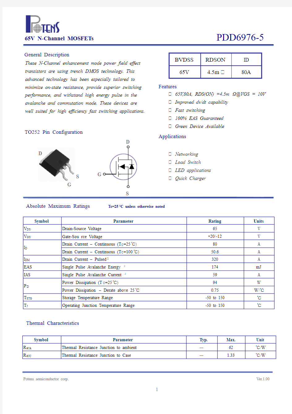
BVDSS RDSON ID 65V
4.5m
80A
Symbol Parameter
Typ. Max. Unit R θJA Thermal Resistance Junction to ambient --- 62 ℃/W R θJC
Thermal Resistance Junction to Case
---
1.33
℃/W
These N-Channel enhancement mode power field effect transistors are using trench DMOS technology. This advanced technology has been especially tailored to minimize on-state resistance, provide superior switching performance, and withstand high energy pulse in the avalanche and commutation mode. These devices are well suited for high efficiency fast switching applications. ● 65V,80A, RDS(ON) =4.5m Ω@VGS = 10V ● Improved dv/dt capability ● Fast switching ● 100% EAS Guaranteed ● Green Device Available
General Description
Features
Applications
Absolute Maximum Ratings Tc=25℃ unless otherwise noted Thermal Characteristics TO252 Pin Configuration
G
S
G
● Networking ● Load Switch
● LED applications ● Quick Charger
D
S
Symbol Parameter
Conditions
Min. Typ. Max. Unit BV DSS
Drain-Source Breakdown Voltage
V GS =0V , I D =250uA 65 --- --- V △BV DSS /△T J BV DSS Temperature Coefficient
Reference to 25℃ , I D =1mA --- 0.02 --- V/℃ I DSS Drain-Source Leakage Current V DS =60V , V GS =0V , T J =25℃ --- --- 1 uA V DS =48V , V GS =0V , T J =85℃ --- --- 10 uA I GSS
Gate-Source Leakage Current
V GS =20V , V DS =0V
---
---
100
nA
On Characteristics
R DS(ON) Static Drain-Source On-Resistance V GS =10V , I D =30A --- 3.7 4.5 m Ω V GS =4.5V , I D =20A --- 5.7 7.5 m Ω V GS(th) Gate Threshold Voltage V GS =V DS , I D =250uA 1 1.5 2.5 V △V GS(th) V GS(th) Temperature Coefficient --- -5.1 --- mV/℃ gfs
Forward Transconductance
V DS =10V , I D =3A
---
12
---
S
Dynamic and switching Characteristics
Q g Total Gate Charge 3 , 4 V DS =48V , V GS =10V , I D =5A
--- 54 108 nC
Q gs Gate-Source Charge 3 , 4 --- 5.2 10.4 Q gd Gate-Drain Charge 3 , 4 --- 16.1 32.2 T d(on) Turn-On Delay Time 3 , 4 V DD =30V , V GS =10V , R G =6Ω I D =1A
--- 10.6 21 ns T r Rise Time 3 , 4
--- 16.5 33 T d(off) Turn-Off Delay Time 3 , 4 --- 48 96 T f Fall Time 3 , 4 --- 78 150 C iss Input Capacitance V DS =25V , V GS =0V , F=1MHz --- 2940 5900 pF C oss Output Capacitance
--- 850 1700 C rss Reverse Transfer Capacitance --- 15 30 R g
Gate resistance
V GS =0V, V DS =0V, F=1MHz ---
1.24
---
Ω
Symbol Parameter
Conditions
Min. Typ. Max. Unit I S Continuous Source Current V G =V D =0V , Force Current --- --- 80 A I SM Pulsed Source Current --- --- 160 A V SD Diode Forward Voltage
V GS =0V , I S =1A , T J =25℃
---
---
1
V
1. Repetitive Rating : Pulsed width limited by maximum junction temperature.
2. V DD =25V,V GS =10V,L=0.1mH,I AS =59A.,R G =25Ω,Starting T J =25℃.
3. The data tested by pulsed , pulse width ≦ 300us , duty cycle ≦ 2%.
4.
Essentially independent of operating temperature.
Electrical Characteristics (T J =25 ℃, unless otherwise noted) Drain-Source Diode Characteristics and Maximum Ratings
I D , C o n t i n u o u s D r a i n C u r r e n t (A )
Fig.1 Continuous Drain Current vs. T C Fig.2 Normalized RDSON vs. T J
N o r m a l i z e d O n R e s i s t a n c e (m )
Fig.3 Normalized Vth vs. T J N o r m a l i z e d G a t e T h r e s h o l d V o l t a g e (V )
Fig.4 Gate Charge Characteristics
V G S , G a t e t o S o u r c e V o l t a g e (V )
T C , Case Temperature (℃) T J , Junction Temperature (℃)
T J , Junction Temperature (℃) Qg , Gate Charge (nC)
I D , D r a i n C u r r e n t (A )
V DS ,Drain to Source V oltage (V )
Fig.5 Typical Output Characteristics
R D S (O N ) , T u r n -O n R e s i s t a n c e (m o h m )
I D , Drain Current (A)
Fig.6 Turn-On Resistance vs. I D
T d(on)
T r T on
T d(off)
T f T off
V GS
90%
10%
Fig.10 Switching Time Waveform
Fig.8 Normalized Transient Impedance
Fig.9 Maximum Safe Operation Area Fig.11 Gate Charge Waveform
N o r m a l i z e d T h e r m a l R e s p o n s e (R θJ C )
I D , D r a i n C u r r e n t (A )
V DS , Drain to Source V oltage (V) Square Wave Pulse Duration (s)
C a p a c i t a n c e (p F )
V DS , Drain to Source V oltage (V )
Fig.7 Capacitance Characteristics
TO252 PACKAGE INFORMATION
Symbol Dimensions In Millimeters Dimensions In Inches
MAX MIN MAX MIN
A 2.400 2.200 0.094 0.087
A1 1.110 0.910 0.044 0.036 A2 0.150 0.000 0.006 0.000
B 6.800 6.400 0.268 0.252
C 0.580 0.450 0.023 0.018
C1 0.580 0.460 0.023 0.018
D 5.500 5.100 0.217 0.201
E 2.386 2.186 0.094 0.086
F 0.940 0.600 0.037 0.024
F1 0.860 0.500 0.034 0.020 L 10.400 9.400 0.409 0.370 L1 3.000 2.400 0.118 0.094 L2 6.200 5.400 0.244 0.213 L3 1.200 0.600 0.047 0.024 θ 9° 3° 9° 3°