INA226
https://www.doczj.com/doc/b9842070.html, SBOS547–JUNE2011
High-or Low-Side Measurement,
Bi-Directional CURRENT/POWER MONITOR with I2C?Interface
Check for Samples:INA226
FEATURES DESCRIPTION
The INA226is a current shunt and power monitor ?SENSES BUS VOLTAGES FROM0V TO+36V
with an I2C interface.The INA226monitors both a ?HIGH-OR LOW-SIDE SENSING
shunt voltage drop and bus supply voltage.?REPORTS CURRENT,VOLTAGE,AND POWER Programmable calibration value,conversion times,
?HIGH ACCURACY:and averaging,combined with an internal multiplier,
enable direct readouts of current in amperes and –0.1%Gain Error(Max)
power in watts.
–10μV Offset(Max)
?CONFIGURABLE AVERAGING OPTIONS The INA226senses current on buses that can vary
from0V to+36V,while the device obtains its power ?16PROGRAMMABLE ADDRESSES
from a single+2.7V to+5.5V supply,drawing a ?OPERATES FROM2.7to5.5V POWER SUPPLY
typical of330μA of supply current.The INA226is ?MSOP-10PACKAGE specified over the operating temperature range
of–40°C to+125°C.The I2C interface features16 APPLICATIONS programmable addresses.
?SERVERS
RELATED PRODUCTS ?TELECOM EQUIPMENT
DESCRIPTION DEVICE ?COMPUTERS
Current/Power Monitor with Watchdog,Peak-Hold,
INA209?POWER MANAGEMENT and Fast Comparator Functions
?BATTERY CHARGERS INA210,INA211,
Zer?-Drift,Low-Cost,Analog Current Shunt Monitor
INA212,INA213,
Series in Small Package
?POWER SUPPLIES
INA214?TEST EQUIPMENT Zer?-Drift,Bi-Directional Current Power Monitor with
INA219
Two-Wire Interface
High or Low Side,Bi-Directional Current/Power
INA220
Monitor with Two-Wire Interface
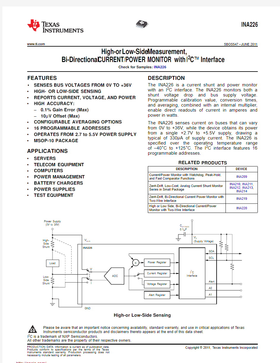
High-or Low-Side Sensing
Please be aware that an important notice concerning availability,standard warranty,and use in critical applications of Texas
Instruments semiconductor products and disclaimers thereto appears at the end of this data sheet.
trademark of NXP Semiconductors.
All other trademarks are the property of their respective owners.
PRODUCTION DATA information is current as of publication date.Copyright?2011,Texas Instruments Incorporated Products conform to specifications per the terms of the Texas
Instruments standard warranty.Production processing does not
necessarily include testing of all parameters.
INA226
SBOS547–https://www.doczj.com/doc/b9842070.html, This integrated circuit can be damaged by ESD.Texas Instruments recommends that all integrated circuits be handled with appropriate precautions.Failure to observe proper handling and installation procedures can cause damage.
ESD damage can range from subtle performance degradation to complete device failure.Precision integrated circuits may be more susceptible to damage because very small parametric changes could cause the device not to meet its published specifications.
PACKAGING INFORMATION(1)
PRODUCT PACKAGE-LEAD PACKAGE DESIGNATOR PACKAGE MARKING
INA226AIDGS MSOP-10DGS226
(1)For the most current package and ordering information see the Package Option Addendum at the end of this document,or see the
INA226product folder at https://www.doczj.com/doc/b9842070.html,.
ABSOLUTE MAXIMUM RATINGS(1)
Over operating free-air temperature range(unless otherwise noted).
INA226UNIT Supply Voltage,V S6V Differential(VIN+)–(VIN–)(2)–40to+40V
Analog Inputs,
VIN+,VIN–Common-Mode–0.3to+40V
SDA GND–0.3to+6V
SCL GND–0.3to V S+0.3V
Input Current Into Any Pin5mA
Open-Drain Digital Output Current10mA Storage Temperature–65to+150°C Junction Temperature+150°C Human Body Model(HBM)2500V
ESD Ratings Charged-Device Model(CDM)1000V Machine Model(MM)150V
(1)Stresses above these ratings may cause permanent damage.Exposure to absolute maximum conditions for extended periods may
degrade device reliability.These are stress ratings only,and functional operation of the device at these or any other conditions beyond those specified is not implied.
(2)VIN+and VIN–may have a differential voltage of–40V to+40V;however,the voltage at these pins must not exceed the range–0.3V to
+40V.
2Submit Documentation Feedback Copyright?2011,Texas Instruments Incorporated
Product Folder Link(s):INA226
INA226
https://www.doczj.com/doc/b9842070.html, SBOS547–JUNE2011
ELECTRICAL CHARACTERISTICS:V S=+3.3V
Boldface limits apply over the specified temperature range,T A=–40°C to+125°C.
At T A=+25°C,VIN+=12V,V SENSE=(VIN+–VIN–)=0mV,V BUS=12V,unless otherwise noted.
INA226
PARAMETER CONDITIONS MIN TYP MAX UNIT INPUT
Shunt voltage input range-81.917581.92mV
Bus voltage input range(1)036V Common-mode rejection CMRR V IN+=0V to+36V126140dB Shunt offset voltage,RTI(2)V OS±2.5±10μV vs Temperature0.020.1μV/°C vs Power supply PSRR V S=+2.7V to+5.5V 2.5μV/V Bus offset voltage,RTI(2)V OS±1.25±7.5mV vs Temperature1040μV/°C vs Power supply PSRR0.5mV/V Input bias current I IN+,I IN-10μA
V BUS input impedance830kΩ
(VIN+Pin)+(VIN–Pin),
Input leakage(3)0.10.5μA
Power-down mode
DC ACCURACY
ADC native resolution16Bits
1LSB step size Shunt voltage 2.5μV
Bus voltage 1.25mV Shunt voltage gain error0.020.1% vs Temperature1050ppm/°C Bus voltage gain error0.020.1% vs Temperature1050ppm/°C Differential nonlinearity±0.1LSB ADC conversion time CT bit=000140154μs
CT bit=001204224μs
CT bit=010332365μs
CT bit=011588646μs
CT bit=100 1.1 1.21ms
CT bit=101 2.116 2.328ms
CT bit=110 4.156 4.572ms
CT bit=1118.2449.068ms SMBus
SMBus timeout(4)2835ms DIGITAL INPUT/OUTPUT
Input capacitance3pF Leakage input current0≤V IN≤V S0.11μA Input logic levels:
V IH0.7(V S)6V V IL–0.50.3(V S)V Output logic level
V OL SDA,alert I OL=3mA00.4V Hysteresis500mV (1)While the input range is36V,the full-scale range of the ADC scaling is40.96V.See the Basic ADC Functions section.Do not apply
more than36V.
(2)RTI=Referred-to-input.
(3)Input leakage is positive(current flowing into the pin)for the conditions shown at the top of this table.Negative leakage currents can
occur under different input conditions.
(4)SMBus timeout in the INA226resets the interface any time SCL is low for more than28ms.
Copyright?2011,Texas Instruments Incorporated Submit Documentation Feedback3
Product Folder Link(s):INA226
INA226
SBOS547–https://www.doczj.com/doc/b9842070.html,
ELECTRICAL CHARACTERISTICS:V S=+3.3V(continued)
Boldface limits apply over the specified temperature range,T A=–40°C to+125°C.
At T A=+25°C,VIN+=12V,V SENSE=(VIN+–VIN–)=0mV,V BUS=12V,unless otherwise noted.
INA226
PARAMETER CONDITIONS MIN TYP MAX UNIT POWER SUPPLY
Operating supply range+2.7+5.5V Quiescent current330420μA Quiescent current,power-down mode0.52μA Power-on reset threshold2V TEMPERATURE RANGE
Specified range–40+125°C
THERMAL INFORMATION
INA226
THERMAL METRIC(1)DGS UNITS
10PINS
θJA Junction-to-ambient thermal resistance171.4
θJCtop Junction-to-case(top)thermal resistance42.9
θJB Junction-to-board thermal resistance91.8
°C/W
ψJT Junction-to-top characterization parameter 1.5
ψJB Junction-to-board characterization parameter90.2
θJCbot Junction-to-case(bottom)thermal resistance n/a
(1)For more information about traditional and new thermal metrics,see the IC Package Thermal Metrics application report,SPRA953.
4Submit Documentation Feedback Copyright?2011,Texas Instruments Incorporated
Product Folder Link(s):INA226
GND V S+
V BUS SCL
12345
109876
A1A0SDA Alert VIN+VIN -
Shunt Voltage
Channel Bus Voltage
Channel
INA226
https://www.doczj.com/doc/b9842070.html,
SBOS547–JUNE 2011
PIN CONFIGURATIONS
DGS PACKAGE
MSOP-10(Top View)
PIN DESCRIPTIONS
MSOP-10(DGS)
PIN NO NAME DESCRIPTION
1A1Address pin.Connect to GND,SCL,SDA,or V S .Table 7shows pin settings and corresponding addresses.2A0Address pin.Connect to GND,SCL,SDA,or V S .Table 7shows pin settings and corresponding addresses.3Alert Multi-functional alert,open-drain output.4SDA Serial bus data line,open-drain input/output.5SCL Serial bus clock line,open-drain input.6V S+Power supply,2.7V to 5.5V.7GND Ground.
8V BUS Bus voltage input.
9VIN –Negative differential shunt voltage.Connect to negative side of shunt resistor.10
VIN+
Positive differential shunt voltage.Connect to positive side of shunt resistor.
REGISTER BLOCK DIAGRAM
(1)Read-only (2)
Read/write
Figure 1.INA226Register Block Diagram
Copyright ?2011,Texas Instruments Incorporated Submit Documentation Feedback
5
Product Folder Link(s):INA226
?60
?50?40?30?20?100110
1001k 10k 100k
Frequency (Hz)
G a i n (d B )
G001
P o p u l a t i o n
-10
-8
-6
-4
-2
2
4
6
8
10
Input Offset Voltage (V)
m ?2.4
?2.2?2?1.8?1.6?1.4?1.2?1?50
?25
255075
100
125
Temperature (°C)
O f f s e t (μV )
G003
140150
160
170?50
?250
255075100
125
Temperature (°C)
C o m m o n ?M o d e R e j e c t i o n R a t i o (d B )
G004
0100200300400500600?50
?250
255075100125
Temperature (°C)
G a i n E r r o r (m %)
G007
P o
p u l a t i o n
-100
-80
-60
-40
-20
20
40
60
80
100
Input Gain Error (m%)
INA226
SBOS547–JUNE 2011
https://www.doczj.com/doc/b9842070.html,
TYPICAL CHARACTERISTICS
At T A =+25°C,V S =+3.3V,VIN+=12V,V SENSE =(VIN+–VIN –)=0mV,V BUS =12V,unless otherwise noted.
SHUNT INPUT OFFSET VOLTAGE FREQUENCY RESPONSE
PRODUCTION DISTRIBUTION
Figure 2.
Figure 3.
SHUNT INPUT OFFSET VOLTAGE
SHUNT INPUT COMMON-MODE REJECTION RATIO
vs TEMPERATURE
vs TEMPERATURE
Figure 4.
Figure 5.
SHUNT INPUT GAIN ERROR PRODUCTION DISTRIBUTION
SHUNT INPUT GAIN ERROR vs TEMPERATURE
Figure 6.
Figure 7.
6Submit Documentation Feedback
Copyright ?2011,Texas Instruments Incorporated
Product Folder Link(s):INA226
?50
0501001502002503000
4
8121620242832
36
Common?Mode Input Voltage (V)
G a i n E r r o r (m %)
G008
P o p u l a t i o n
-7.5
-6
-4.5
-3
-1.5
1.5
3
4.5
67.5
Input Offset Voltage (mV)
?1.4
?1.2
?1.0
?0.8?0.6
?50
?250
255075100125
Temperature (°C)
O f f s e t (m V )
G009
P o p u l a t i o n
-100
-8
-60
-40
-20
20
40
60
80100Input Gain Error (m%)
0100200300400500600?50
?250
255075100125
Temperature (°C)
G a i n E r r o r (m %)
G012
5
10
15
20
25
04
8121620242832
36
Common?Mode Input Voltage (V)
I n p u t B i a s C u r r e n t (μA )
G012
INA226
https://www.doczj.com/doc/b9842070.html,
SBOS547–JUNE 2011
TYPICAL CHARACTERISTICS (continued)
At T A =+25°C,V S =+3.3V,VIN+=12V,V SENSE =(VIN+–VIN –)=0mV,V BUS =12V,unless otherwise noted.
SHUNT INPUT GAIN ERROR BUS INPUT OFFSET VOLTAGE vs COMMON-MODE VOLTAGE
PRODUCTION DISTRIBUTION
Figure 8.
Figure 9.
BUS INPUT OFFSET VOLTAGE vs TEMPERATURE
BUS INPUT GAIN ERROR PRODUCTION DISTRIBUTION
Figure 10.
Figure 11.
BUS INPUT GAIN ERROR vs TEMPERATURE
INPUT BIAS CURRENT vs COMMON-MODE VOLTAGE
Figure 12.
Figure 13.
Copyright ?2011,Texas Instruments Incorporated Submit Documentation Feedback
7
Product Folder Link(s):INA226
1618
20
22
24
?50
?25
255075
100
125
Temperature (°C)
I n p u t B i a s C u r r e n t (μA )
G013
2060100140180220260?50
?250
255075100125
Temperature (°C)
I n p u t B i a s C u r r e n t ? S h u t d o w n (n A )
G014
100200
300
400
500
?50
?250
255075100125
Temperature (°C)
Q u i e s c e n t C u r r e n t (μA )
G015
0.20.4
0.6
0.8
1
1.2
?50
?250
255075100125
Temperature (°C)
Q u i e s c e n t C u r r e n t ? S h u t d o w n (μA )
G016
1
10
1001,000
10,000
Frequency (kHz)
500
450
400
350
300
I (A )
Q
m 1
10
1001,000
10,000
Frequency (kHz)
300250
20015010050
0S h u t d o w n I (A )
Q m INA226
SBOS547–JUNE 2011
https://www.doczj.com/doc/b9842070.html,
TYPICAL CHARACTERISTICS (continued)
At T A =+25°C,V S =+3.3V,VIN+=12V,V SENSE =(VIN+–VIN –)=0mV,V BUS =12V,unless otherwise noted.
INPUT BIAS CURRENT vs TEMPERATURE
INPUT BIAS CURRENT vs TEMPERATURE,SHUTDOWN
Figure 14.
Figure 15.
ACTIVE I Q vs TEMPERATURE
SHUTDOWN I Q vs TEMPERATURE
Figure 16.
Figure 17.
ACTIVE I Q vs I 2C CLOCK FREQUENCY
SHUTDOWN I Q vs I 2C CLOCK FREQUENCY
Figure 18.Figure 19.
8Submit Documentation Feedback
Copyright ?2011,Texas Instruments Incorporated
Product Folder Link(s):INA226
INA226
https://www.doczj.com/doc/b9842070.html, SBOS547–JUNE2011
APPLICATION INFORMATION
The INA226is a digital current shunt monitor with an I2C-and SMBus-compatible interface.It provides digital current,voltage,and power readings necessary for accurate decision-making in precisely-controlled systems. Programmable registers allow flexible configuration for measurement resolution as well as continuous-versus-triggered operation.Detailed register information appears at the end of this data sheet, beginning with Table2.See the Register Block Diagram for a block diagram of the INA226.
INA226TYPICAL APPLICATION
The front-page figure shows a typical application circuit for the https://www.doczj.com/doc/b9842070.html,e a0.1μF ceramic capacitor for power-supply bypassing,placed as closely as possible to the supply and ground pins.
BASIC ADC FUNCTIONS
The INA226performs two measurements on the power-supply bus of interest.The voltage developed from the load current that flows through a shunt resistor creates a shunt voltage that is measured at the VIN+and VIN–pins.The device can also measure the power supply bus voltage by connecting this voltage to the V BUS pin.The differential shunt voltage is measured with respect to the VIN–pin while the bus voltage is measured with respect to ground.
The INA226is typically powered by a separate supply that can range from2.7V to5.5V.The bus that is being monitored can range in voltage from0V to36V.It is important to note here that based on the fixed1.25mV LSB for the bus voltage register that a full-scale register would result in a40.96V value.The actual voltage that is applied to the input pins of the INA226should not exceed36V.There are no special considerations for power-supply sequencing because the common-mode input range and power-supply voltage are independent of each other;therefore,the bus voltage can be present with the supply voltage off,and vice-versa.
As noted,the INA226takes two measurements,shunt voltage and bus voltage.It then converts these measurements to current,based on the Calibration Register value,and then calculates power.Refer to the Configure/Measure/Calculate Example section for additional information on programming the Calibration Register.
The INA226has two operating modes,continuous and triggered,that determine how the ADC operates following these conversions.When the INA226is in the normal operating mode(that is,MODE bits of the Configuration Register are set to'111'),it continuously converts a shunt voltage reading followed by a bus voltage reading. After the shunt voltage reading,the current value is calculated(based on Equation3).This current value is then used to calculate the power result(using Equation4).These values are subsequently stored in an accumulator, and the measurement/calculation sequence repeats until the number of averages set in the Configuration Register is reached.Following every sequence,the present set of values measured and calculated are appended to previously collected values.Once all of the averaging has been completed,the final values for shunt voltage,bus voltage,current,and power are updated in the corresponding registers that can then be read. These values remain in the data output registers until they are replaced by the next fully completed conversion results.Reading the data output registers does not affect a conversion in progress.
The Mode control in the Configuration Register also permits selecting modes to convert only the shunt voltage or the bus voltage in order to further allow the user to configure the monitoring function to fit the specific application requirements.
All current and power calculations are performed in the background and do not contribute to conversion time.
In triggered mode,writing any of the triggered convert modes into the Configuration Register(that is,MODE bits of the Configuration Register are set to‘001’,‘010’,or‘011’)triggers a single-shot conversion.This action produces a single set of measurements;thus,to trigger another single-shot conversion,the Configuration Register must be written to a second time,even if the mode does not change.
In addition to the two operating modes(continuous and triggered),the INA226also has a power-down mode that reduces the quiescent current and turns off current into the INA226inputs,reducing the impact of supply drain when the device is not being used.Full recovery from power-down mode requires40ms.The registers of the INA226can be written to and read from while the device is in power-down mode.The device remains in power-down mode until one of the active modes settings are written into the Configuration Register.
Copyright?2011,Texas Instruments Incorporated Submit Documentation Feedback9
Product Folder Link(s):INA226
P
P
P
P
P
P
P
P
P
P
P
P
P
P
P
P
Current Limit Detect Following Every Shunt Voltage Conversion
Bus and Power Limit Detect
Following Every Bus Voltage Conversion
INA226
SBOS547–JUNE 2011
https://www.doczj.com/doc/b9842070.html,
Although the INA226can be read at any time,and the data from the last conversion remain available,the Conversion Ready Flag bit (Mask/Enable Register,CVRF bit)is provided to help coordinate one-shot or triggered conversions.The Conversion Ready Flag bit is set after all conversions,averaging,and multiplication operations are complete.
The Conversion Ready Flag bit clears under these conditions:
1.Writing to the Configuration Register,except when configuring the MODE bits for power-down mode;or
2.Reading the Status Register.Power Calculation
The Current and Power are calculated following shunt voltage and bus voltage measurements as shown in Figure 20.Current is calculated following a shunt voltage measurement based on the value set in the Calibration Register.If there is no value loaded into the Calibration Register,the current value stored is zero.Power is calculated following the bus voltage measurement based on the previous current calculation and bus voltage measurement.If there is no value loaded in the Calibration Register,the power value stored is also zero.Again,these calculations are performed in the background and do not add to the overall conversion time.These current and power values are considered intermediate results (unless the averaging is set to 1)and are stored in an internal accumulation register,not the corresponding output registers.Following every measured sample,the newly-calculated values for current and power are appended to this accumulation register until all of the samples have been measured and averaged based on the number of averages set in the Configuration Register.
Figure 20.Power Calculation Scheme
In addition to the current and power accumulating after every sample,the shunt and bus voltage measurements are also collected.Once all of the samples have been measured and the corresponding current and power calculations have been made,the accumulated average for each of these parameters is then loaded to the corresponding output registers,where they can then be read.
10Submit Documentation Feedback
Copyright ?2011,Texas Instruments Incorporated
Product Folder Link(s):INA226
分销商库存信息:
TI
INA226AIDGSR INA226AIDGST INA226EVM