CIBH Diode with Superior Soft Switching Behavior
in 3.3kV Modules for Fast Switching Applications
Jürgen Biermann, Infineon Technologies AG, Max-Planck-Strasse 5, D-59581 Warstein, Germany Manfred Pfaffenlehner, Infineon Technologies AG, Am Campeon 1-12, D-85579 Neubiberg, Germany Hans Peter Felsl, Infineon Technologies AG, Am Campeon 1-12, D-85579 Neubiberg, Germany Thomas Gutt, Infineon Technologies AG, Am Campeon 1-12, D-85579 Neubiberg, Germany
Holger Schulze, Infineon Technologies Austria AG, Siemensstrasse 2, A-9500 Villach, Austria
Abstract
A new technology for the vertical architecture of free wheeling diodes (FWDs) is introduced, which is optimized for applications with high switching frequencies. To minimize the turn off losses of the diode and the turn on losses of the IGBT, for the first time a diode with the CIBH (Controlled Injection of Backside Holes) concept is implemented.
The CIBH diode allows to reduce the charge stored in the diode by minimizing the wafer thickness and reducing the doping concentration of the backside emitter, whereas an excellent switching softness remains even under extreme switching conditions. The advantage of the CIBH technology for high power applications is shown by investigations in IHV modules with 1500A current rating and compari-sons to state-of-the-art FWDs.
1 Motivation
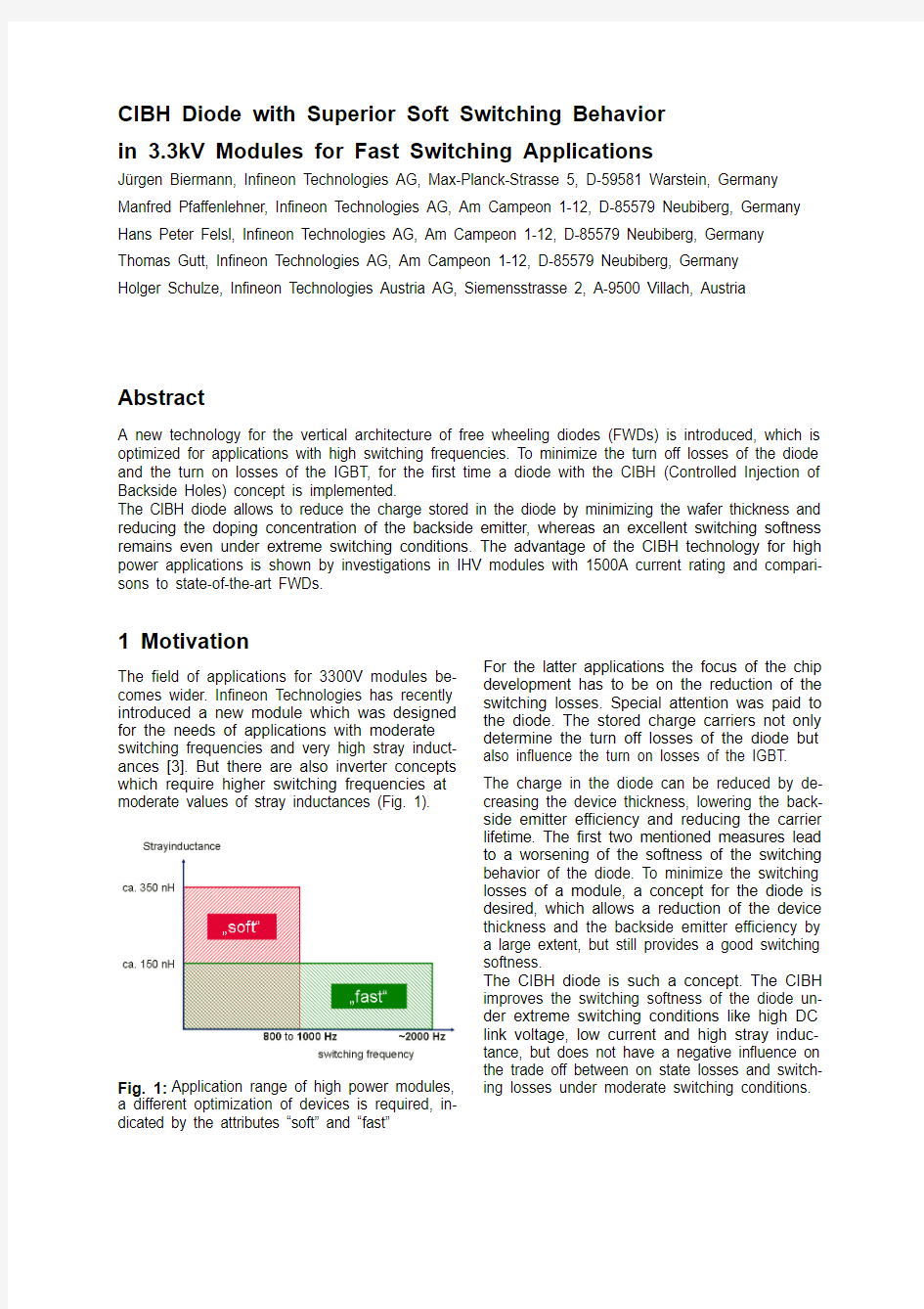
The field of applications for 3300V modules be-comes wider. Infineon Technologies has recently introduced a new module which was designed for the needs of applications with moderate switching frequencies and very high stray induct-ances [3]. But there are also inverter concepts which require higher switching frequencies at moderate values of stray inductances (Fig. 1).
Fig. 1: Application range of high power modules, a different optimization of devices is required, in-dicated by the attributes “soft” and “fast” For the latter applications the focus of the chip development has to be on the reduction of the switching losses. Special attention was paid to the diode. The stored charge carriers not only determine the turn off losses of the diode but also influence the turn on losses of the IGBT.
The charge in the diode can be reduced by de-creasing the device thickness, lowering the back-side emitter efficiency and reducing the carrier lifetime. The first two mentioned measures lead to a worsening of the softness of the switching behavior of the diode. To minimize the switching losses of a module, a concept for the diode is desired, which allows a reduction of the device thickness and the backside emitter efficiency by a large extent, but still provides a good switching softness.
The CIBH diode is such a concept. The CIBH improves the switching softness of the diode un-der extreme switching conditions like high DC link voltage, low current and high stray induc-tance, but does not have a negative influence on the trade off between on state losses and switch-ing losses under moderate switching conditions.
2 The CIBH Concept
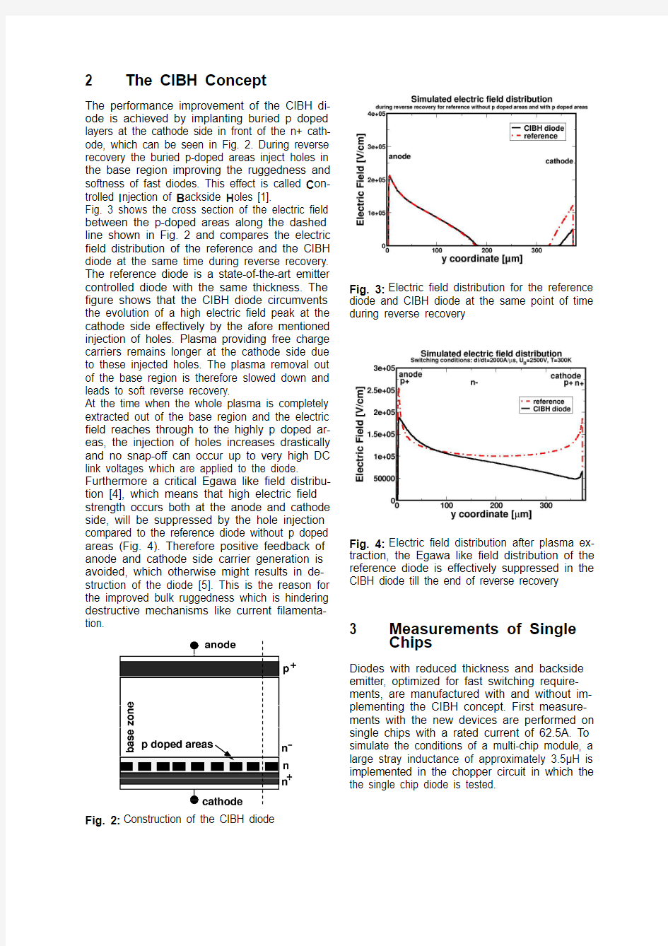
The performance improvement of the CIBH di-ode is achieved by implanting buried p doped layers at the cathode side in front of the n+ cath-ode, which can be seen in Fig. 2. During reverse recovery the buried p-doped areas inject holes in the base region improving the ruggedness and softness of fast diodes. This effect is called C on-trolled I njection of B ackside H oles [1].
Fig. 3 shows the cross section of the electric field between the p-doped areas along the dashed line shown in Fig. 2 and compares the electric field distribution of the reference and the CIBH diode at the same time during reverse recovery. The reference diode is a state-of-the-art emitter controlled diode with the same thickness. The figure shows that the CIBH diode circumvents the evolution of a high electric field peak at the cathode side effectively by the afore mentioned injection of holes. Plasma providing free charge carriers remains longer at the cathode side due to these injected holes. The plasma removal out of the base region is therefore slowed down and leads to soft reverse recovery.
At the time when the whole plasma is completely extracted out of the base region and the electric field reaches through to the highly p doped ar-eas, the injection of holes increases drastically and no snap-off can occur up to very high DC link voltages which are applied to the diode. Furthermore a critical Egawa like field distribu-tion [4], which means that high electric field strength occurs both at the anode and cathode side, will be suppressed by the hole injection compared to the reference diode without p doped areas (Fig. 4). Therefore positive feedback of anode and cathode side carrier generation is avoided, which otherwise might results in de-struction of the diode [5]. This is the reason for the improved bulk ruggedness which is hindering destructive mechanisms like current filamenta-tion.
Fig. 2: Construction of the CIBH diode
Fig. 3: Electric field distribution for the reference diode and CIBH diode at the same point of time during reverse recovery
Fig. 4: Electric field distribution after plasma ex-traction, the Egawa like field distribution of the reference diode is effectively suppressed in the CIBH diode till the end of reverse recovery
3 Measurements of Single
Chips
Diodes with reduced thickness and backside emitter, optimized for fast switching require-ments, are manufactured with and without im-plementing the CIBH concept. First measure-ments with the new devices are performed on single chips with a rated current of 62.5A. To simulate the conditions of a multi-chip module, a large stray inductance of approximately 3.5μH is implemented in the chopper circuit in which the the single chip diode is tested.
At 2/10 of the rated current and at low device temperature the DC link voltage is increased step by step.
V CE = 2050V
V CE = 2250V
Fig. 5: reverse recovery behavior of reference
diode
V CE = 2050V
V CE = 2250V
voltage current
V CE = 2450V
Fig. 6: reverse recovery behavior of CIBH diode
Fig. 5 and 6 show a comparison of the switching wave forms of a reference diode and a diode with the CIBH concept. Both diodes have the same thickness. The reference diode shows a massive current snap off and voltage oscillations starting below 2000V. The amplitude of the oscil-lations increase as the DC link voltage is in-creased. The measurements were stopped to avoid a voltage overshoot above the rated value of 3300V.
The CIBH diode shows no oscillations up to ap-proximately 2100V. Above that level some small oscillations can be observed. The amplitude of these oscillations is not increasing with increas-ing DC link voltage, but the oscillations disappear with further increase of the DC link voltage. The oscillations are suppressed by the hole injection from the structured p-doped areas in the back-side of the device. These additional charge carri-ers which are provided can be seen in the cur-rent waveforms of Fig. 6. The current tail during reverse recovery does not decrease, in contrast the tail increases when applying high DC link voltages. With further optimization also the small remaining oscillations can be avoided.
This effect we have called D ynamic S elf D amp-ing M ode [6]. The effect suppresses oscillations and provides in a self adjusting way enough charge carriers to avoid effectively snap off un-der extreme switching conditions.
4 Module Measurements
As the next step a 140x190mm 2 high voltage module with 24 diodes in parallel and a rated current of 1500A is investigated. In this large module the advantages of the CIBH concept be-come obvious. Fig. 7 shows a CIBH diode re-covery under extreme switching conditions. Normally high values of stray inductance (L S = 320nH) and DC link voltage (V CE = 2300V) com-bined with low temperature (T = 25°C) and low
current (I CE = 300A) lead to a massive current snap off and oscillations at a state-of-the-art fast diode opimized for low switching losses.
In contrast the paralleled CIBH diodes show a very soft switching behavior even at a high DC link voltage and with a stray inductance well above the required level. So the current cut off - self protection allows to design in this diode into applications with high stray inductances.
Fig. 7: Diode recovery of a 1500A rated current module under extreme switching conditions, V CE =2300V, L S = 320nH, T=25°C, I=300A
Further quantitative analysis of the improved trade off between softness on the one side and dynamic and static losses on the other side is shown in Fig. 8. The advantages of the thin CIBH diode can be clearly seen in a direct comparison with a soft reference diode, having high reverse recovery losses. The fast CIBH diode provides the same soft switching behavior as the soft ref-erence diode.
Fig. 8: Trade-off diode switching losses vs. on state losses
In inverters with higher stray inductances it is possible to reduce the diode switching losses by 25% with the same on state losses. This leads
consequently to reduced IGBT turn on losses at the same time.
The introduction of a new diode concept required the complete program of characterisation and reliability tests. Hence a lot of investigations on ruggedness under hard switching conditions cov-ering wide temperature range were performed.
Fig. 9: Diode recovery of a 1500A module with excellent robustness; V DC =2400V, I=3000A, L S = 95nH, P diode =15.3MW
Fig. 9 shows a diode recovery which is done un-der test conditions far above from the real appli-cation conditions. Peak power values above 15.3MW with FZ1500R33HE3 modules have been reached without destruction. The test con-ditions are V CE =2400V, I CE =2*Inom=3000A and a module temperature of T j =150°C. The results guarantee a large safety margin to the datasheet peak power values.
5 Conclusion
For the first time a module with a CIBH diode has been successfully introduced. This diode con-cept leads to a great reduction of the turn off losses of the diode and the turn on losses of the IGBT, but still offers a very soft switching behav-ior even under extreme switching conditions due to the DSDM (Dynamic Self Damping Mode). The new diode concept is a breakthrough solu-tion for FWDs in modern high power / high volt-age inverters. In combination with IGBT3 [2] with trench cell and field stop technology a new benchmark is set in both softness and minimal total losses for high power IGBT modules.
6 Acknowledgement
We acknowledge M. Chen and J. Lutz, chair for power electronics and electromagnetic compati-bility from the Technical University of Chemnitz for discussions and contributions to the CIBH concept and simulations concerning the principal device behavior.
7 Literature
[1] M.Chen, J. Lutz, M. Domeij, H.P. Felsl, H.-J.
Schulze, A Novel Diode Structure with Con-
trolled Injection of Backside Holes (CIBH),
Proc. ISPSD’06, pp. 9-12, Naples, Italy, Ju-
ne 2006.
[2] M. Pfaffenlehner, J. Biermann, C. Sch?ffer,
H. Schulze: New 3300V Chip Generation
with a Trench IGBT and an Optimized Field
Stop Concept with a Smooth Switching Be-
havior, Proc. ISPSD’04, pp. 107 – 110, Kita-
kyushu, Japan, May 2004
[3] J. Biermann, M. Pfaffenlehner, C. Sch?ffer,
H. Schulze: New 3300V Trench IGBT Modu-
le for Highest Converter Efficiency, Proc.
PCIM, 2004, Nuremberg, Germany
[4] H. Egawa, Avalanche Characteristics and
Failure Mechanism of High Voltage Diodes,
IEEE Transaction on Electron Devices, Vol.
13, No. 11, November 1966
[5] M. Domeij; J. Lutz, D. Silber, “On the De-
struction Limit of Si Power Diodes During reverse Recovery with Dynamic Avalanche”,
IEEE Trans.El. Devices, vol. 50 no.2, 2003,
pp. 486-493.
[6] H. P. Felsl, M. Pfaffenlehner, H. Schulze, J.
Biermann, Th. Gutt, H.-J. Schulze, M. Chen,
J. Lutz, “The CIBH Diode – Great Improve-
ment for Ruggedness and Softness of High
Voltage Diodes”, to be published at the 20th
ISPSD 2008, Orlando, Forida.