General Description
The MAX1153/MAX1154 are stand-alone, 10-channel (8external, 2 internal) 10-bit system monitor ADCs with internal reference. A programmable single-ended/dif-ferential mux accepts voltage and remote-diode tem-perature-sensor inputs. These devices independently monitor the input channels without microprocessor interaction and generate an interrupt when any variable exceeds user-defined limits. The MAX1153/MAX1154configure both high and low limits, as well as the num-ber of fault cycles allowed, before generating an inter-rupt. These ADCs can also perform recursive data averaging for noise reduction. Programmable wait inter-vals between conversion sequences allow the selection of the sample rate.
At the maximum sampling rate of 94ksps (auto mode,single channel enabled), the MAX1153 consumes only 5mW (1.7mA at 3V). AutoShutdown TM reduces supply current to 190μA at 2ksps and to less than 8μA at 50sps.Stand-alone operation, combined with ease of use in a small package (16-pin TSSOP), makes the MAX1153/MAX1154 ideal for multichannel system-monitoring applications. Low power consumption also makes these devices a good fit for hand-held and battery-pow-ered applications.
Applications
System Supervision Remote Telecom Networks Server Farms Remote Data Loggers
Features
?Monitor 10 Signals Without Processor Intervention
?Eight External Channels Programmable as Temperature or Voltage Monitors
?Intelligent Circuitry for Reliable Autonomous Measurement
Programmable Digital Averaging Filter Programmable Fault Counter ?Precision Measurements
10-Bit Resolution
±0.5 LSB INL, ±0.5 LSB DNL
±0.75°C Temperature Accuracy (typ)?Flexible
Automatic Channel Scan Sequencer with Programmable Intervals
Programmable Inputs: Single Ended/Differential,Voltage/Temperature
Programmable Wait State ?Internal 2.5V/4.096V Reference (MAX1153/MAX1154)
?Remote Temperature Sensing Up to 10m (Differential Mode)
?Single 3V or 5V Supply Operation ?Small 16-Pin TSSOP Package
MAX1153/MAX1154
Stand-Alone, 10-Channel, 10-Bit System Monitors with Internal T emperature Sensor and V DD Monitor
________________________________________________________________Maxim Integrated Products 1
19-2839; Rev 1; 6/10
For pricing, delivery, and ordering information,please contact Maxim Direct at 1-888-629-4642,or visit Maxim’s website at https://www.doczj.com/doc/d83502217.html,.
Typical Application Circuit appears at end of data sheet.AutoShutdown is a trademark of Maxim Integrated Products, Inc.
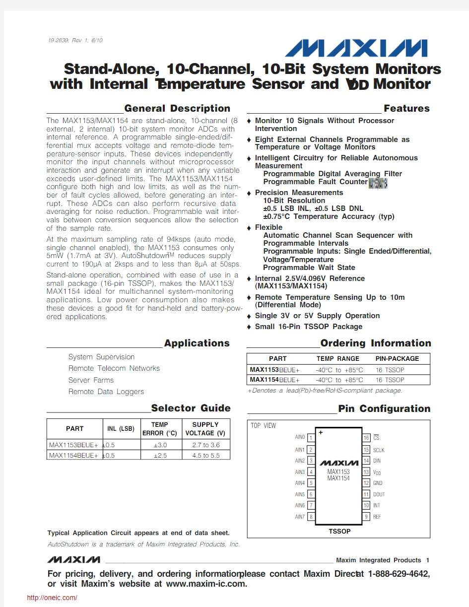
Pin Configuration
Ordering Information
+Denotes a lead(Pb)-free/RoHS-compliant package.
M A X 1153/M A X 1154
Stand-Alone, 10-Channel, 10-Bit System Monitors with Internal T emperature Sensor and V DD Monitor
ABSOLUTE MAXIMUM RATINGS
Stresses beyond those listed under “Absolute Maximum Ratings” may cause permanent damage to the device. These are stress ratings only, and functional operation of the device at these or any other conditions beyond those indicated in the operational sections of the specifications is not implied. Exposure to absolute maximum rating conditions for extended periods may affect device reliability.
V DD to GND.............................................................-0.3V to +6V Analog Inputs to GND (AIN0–AIN7, REF) ...-0.3V to (V DD + 0.3V)Digital Inputs to GND (DIN, SCLK, CS ) ....-0.3V to (V DD + 0.3V)Digital Outputs to GND (DOUT, INT) ........-0.3V to (V DD + 0.3V)Digital Outputs Sink Current .............................................25mA Maximum Current into Any Pin ..........................................50mA Continuous Power Dissipation (T A = +70°C)
16-Pin TSSOP (derate 11.1mW/°C above +70°C).......889mW
Operating Temperature Range ...........................-40°C to +85°C Junction Temperature......................................................+150°C Storage Temperature Range.............................-65°C to +150°C Lead Temperature (soldering, 10s).................................+300°C Soldering Temperature (reflow).......................................+260°C
ELECTRICAL CHARACTERISTICS
MAX1153/MAX1154
Stand-Alone, 10-Channel, 10-Bit System Monitors with Internal T emperature Sensor and V DD Monitor
_______________________________________________________________________________________3
ELECTRICAL CHARACTERISTICS (continued)
M A X 1153/M A X 1154
Stand-Alone, 10-Channel, 10-Bit System Monitors with Internal T emperature Sensor and V DD Monitor 4_______________________________________________________________________________________
ELECTRICAL CHARACTERISTICS (continued)
MAX1153/MAX1154
Stand-Alone, 10-Channel, 10-Bit System Monitors with Internal T emperature Sensor and V DD Monitor
_______________________________________________________________________________________5
TIMING CHARACTERISTICS
Note 2:Relative accuracy is the deviation of the analog value at any code from its theoretical value after the gain and offset errors have been calibrated.Note 3:Offset nulled.
Note 4:
In reference mode 00, the reference system powers up for each temperature measurement. In reference mode 01, the ref-erence system powers up once per sequence of channels scanned. If a sample wait <80μs is programmed, the reference system is on all the time. In reference mode 10, the reference system is on all the time (see Table 7).Note 5:No external capacitor on REF.
Note 6:The operational input voltage range for each individual input of a differentially configured pair (AIN0–AIN7) is from GND to V DD . The operational input voltage difference is from -V REF /2 to +V REF /2.
Note 7:See Figure 3 and the Sampling Error vs. Input Source Impedance graph in the Typical Operating Characteristics section.Note 8:Grade A tested at +10°C and +55°C. -20°C to +85°C and -40°C to +85°C specifications guaranteed by design. Grade B tested at +25°C. T MIN to T MAX specification guaranteed by design.
Note 9:External temperature measurement mode using an MMBT3904 (Diodes Inc.) as a sensor. External temperature sensing from -40°C to +85°C; MAX1153/MAX1154 held at +25°C.
Note 10:Performing eight single-ended external channels’ temperature measurements, an internal temperature measurement, and an internal V DD measurement with no sample wait results in a conversion rate of 2ksps per channel.
Note 11:Performing eight single-ended voltage measurements, an internal temperature measurement, and an internal V DD mea-surement with no sample wait results in a conversion rate of 7ksps per channel.
Note 12:Performing eight single-ended voltage measurements, an internal temperature measurement, and an internal V DD mea-surement with maximum sample wait results in a conversion rate of 3ksps per channel.
Note 13:
Defined as the shift in the code boundary as a result of supply voltage change. V DD = min to max; full-scale input, mea-sured using external reference.
M A X 1153/M A X 1154
Stand-Alone, 10-Channel, 10-Bit System Monitors with Internal T emperature Sensor and V DD Monitor 6_______________________________________________________________________________________
Typical Operating Characteristics
(V DD = +3V, V REF = +2.5V (MAX1153); V DD = +5V, V REF = +4.096V (MAX1154); f SCLK = 10MHz, C REF = 0.1μF, T A = +25°C, unless otherwise noted.)
INTEGRAL NONLINEARITY vs. DIGITAL OUTPUT CODE
M A X 1153/54 t o c 01
OUTPUT CODE
I N L (L S B )
768
512256
-0.40-0.30-0.20-0.1000.100.20
0.300.400.50-0.50
1024
DIFFERENTIAL NONLINEARITY vs. DIGITAL OUTPUT CODE
M A X 1153/54 t o c 02
OUTPUT CODE
D N L (L S B )
768512256-0.40-0.30-0.20-0.1000.100.200.300.400.50-0.50
1024INTERNAL REFERENCE VOLTAGE
vs. SUPPLY VOLTAGE
SUPPLY VOLTAGE (V)
I N T E R N A L R E F E R E N C E V O L T A G E (V )
3.53.43.2 3.32.9 3.0 3.12.82.5012.502
2.5032.5042.5052.5062.5072.5082.5092.5102.500
2.7
3.6
INTERNAL REFERENCE VOLTAGE
vs. SUPPLY VOLTAGE
SUPPLY VOLTAGE (V)
I N T E R N A L R E F E R E N C E V O L T A G E (V )
5.45.35.1 5.24.7 4.8 4.9
5.04.64.077
4.079
4.081
4.083
4.0854.075
4.5
5.5
REFERENCE VOLTAGE vs. TEMPERATURE
TEMPERATURE (°C)
R E F E R E N C E V O L T A G E (V )60
40
20
-20
2.496
2.4972.4982.4992.5002.5012.5022.5032.5042.505
2.495
-40
80
REFERENCE VOLTAGE vs. TEMPERATURE
TEMPERATURE (°C)R E F E R E N C E V O L T A G E (V )60
40
20
-20
4.07254.07504.07754.08004.08254.08504.08754.09004.0700
-40
80
SUPPLY CURRENT vs. SAMPLE RATE
SAMPLE RATE (kHz)
S U P P L Y C U R R E N T (m A )
10
1
0.1
0.01
0.01
0.1
1
10
0.001
0.001
100
MAX1153/MAX1154
Stand-Alone, 10-Channel, 10-Bit System Monitors with Internal T emperature Sensor and V DD Monitor
_______________________________________________________________________________________7
Typical Operating Characteristics (continued)
(V DD = +3V, V REF = +2.5V (MAX1153); V DD = +5V, V REF = +4.096V (MAX1154); f SCLK = 10MHz, C REF = 0.1μF, T A = +25°C, unless otherwise noted.)
SUPPLY CURRENT vs. SAMPLE RATE
SAMPLE RATE (kHz)S U P P L Y C U R R E N T (m A )
10
1
0.1
0.01
0.01
0.1
1
10
0.001
0.001
100
SUPPLY CURRENT vs. SUPPLY VOLTAGE
SUPPLY VOLTAGE (V)S U P P L Y C U R R E N T (m A )
5.1
4.7
3.1
3.5
3.9
4.3
1.41.8
2.22.6
3.03.43.8
4.21.0
2.7
5.5
SUPPLY CURRENT vs. SUPPLY VOLTAGE
SUPPLY VOLTAGE (V)
S U P P L Y C U R R E N T (m A )
5.1
4.7
3.1
3.5
3.9
4.3
1.9
2.32.7
3.13.53.9
4.31.5
2.7
5.5
SUPPLY CURRENT vs. TEMPERATURE
TEMPERATURE (°C)
S U P P L Y C U R R E N T (m A )
80
65
35
50
-10
5
20
-251.71.81.92.02.12.22.32.42.52.61.6
-40
SUPPLY CURRENT vs. TEMPERATURE
TEMPERATURE (°C)S U P P L Y C U R R E N T (m A )
80653550-10520-252.53.04.0
3.5
4.5
5.02.0
-40SHUTDOWN SUPPLY CURRENT
vs. SUPPLY VOLTAGE
SUPPLY VOLTAGE (V)
S H U T D O W N S U P P L Y C U R R E N T (n A )
5.14.74.33.93.53.1200
300400500600700100
2.7 5.5
SHUTDOWN SUPPLY CURRENT
vs. TEMPERATURE
TEMPERATURE (°C)S H U T D O W N S U P P L Y C U R R E N T (n A )
65
50
35
20
5
-10
-251002003004005006007000
-4080
GAIN AND OFFSET ERROR vs. SUPPLY VOLTAGE
SUPPLY VOLTAGE (V)G A I N A N D O F F S E T E R R O R (L S B )
5.14.73.9 4.33.53.1-0.80-0.60-0.40-0.2000.20
0.400.600.801.00-1.00
2.7 5.5GAIN ERROR vs. TEMPERATURE
TEMPERATURE (°C)
G A I N E R R O R (L S B )
80
655035205-10-25-0.0500.050.100.150.200.25-0.10
-40
M A X 1153/M A X 1154
Stand-Alone, 10-Channel, 10-Bit System Monitors with Internal T emperature Sensor and V DD Monitor 8_______________________________________________________________________________________
OFFSET ERROR vs. TEMPERATURE
TEMPERATURE (°C)
O F F S E T E R R O R (L S B )
80
655035205-10-25-0.20-0.15-0.10-0.0500.050.100.150.200.25-0.25
-40
INTERNAL TEMPERATURE SENSOR
TEMPERATURE ERROR
TEMPERATURE (°C)
E R R O R (°C )
60
40
20
-20
-0.80
-0.60-0.40-0.2000.200.400.600.801.00
-1.00
-40
80
EXTERNAL TEMPERATURE SENSOR
TEMPERATURE ERROR
TEMPERATURE (°C)
E R R O R (°C )
60
40
20
-20
-1.60-1.20-0.80-0.4000.400.801.201.602.00
-2.00
-40
80
TEMPERATURE ERROR vs. INTERCONNECT CAPACITANCE (EXTERNAL SENSOR)
M A X 1153/54 t o c 19
INTERCONNECT CAPACITANCE (pF)
T E
M P E R A T U R E (°C )
-5-4-3-2-101-6100
1000SAMPLING ERROR
vs. INPUT SOURCE IMPEDANCE
M A X 1153/54 t o c 20
SOURCE IMPEDANCE (Ω)
S A M P L I N G E R R O R (L S B )
1000100-4-3-2-101-5
1010,000
TURN ON THERMAL TRANSIENT, CONTINUOUS CONVERSION
V
DD = 3.0V
TIME (s)
T E M P E R A T U R E S H I F T (°C )25
20
1510
5
00.125
0.2500.3750.5000.625
-0.125
30
Typical Operating Characteristics (continued)
(V DD = +3V, V REF = +2.5V (MAX1153); V DD = +5V, V REF = +4.096V (MAX1154); f SCLK = 10MHz, C REF = 0.1μF, T A = +25°C, unless otherwise noted.)
MAX1153/MAX1154
Stand-Alone, 10-Channel, 10-Bit System Monitors with Internal T emperature Sensor and V DD Monitor
Block Diagram
M A X 1153/M A X 1154
Stand-Alone, 10-Channel, 10-Bit System Monitors with Internal T emperature Sensor and V DD Monitor 10
______________________________________________________________________________________
Detailed Description
The MAX1153/MAX1154 are precision-monitoring inte-grated circuit systems specifically intended for stand-alone operation. They can monitor diverse types of inputs, such as those from temperature sensors and voltage signals from pressure, vibration, and accelera-tion sensors, and digitize these input signals. The digi-tal values are then compared to preprogrammed thresholds and, if the thresholds are exceeded, the processor is alerted by an interrupt signal. No interac-tion by the CPU or microcontroller (μC) is required until one of the programmed limits is exceeded (F igures 3and 4).
Voltages on all the inputs are converted to 10-bit values sequentially and stored in the current data registers.Note that eight of these inputs are external and two are internal. One of the internal inputs monitors the V DD voltage supply, while the other monitors the internal IC temperature. AIN0 to AIN7 can be configured as either single ended (default) or differential. In addition, these inputs can be configured for single-ended or differen-tial temperature measurements. In the temperature configuration, the device provides the proper bias nec-essary to measure temperature with a diode-connected transistor sensor. The user enables which inputs are measured (both external and internal) and sets the delay between each sequence of measurements dur-ing the initial setup of the device.
The values stored in the current data registers are com-pared to the user-preprogrammed values in the thresh-old registers (upper and lower thresholds) and, if exceeded, activate the interrupt output and generate an
alarm condition. If desired, the device can be pro-grammed to average the results of many measurements before comparing to the threshold value. This reduces the sensitivity to external noise in the measured signal.In addition, the user can set the number of times the threshold is exceeded (fault cycles) before generating an interrupt. This feature reduces falsely triggered alarms caused by undesired, random spurious impulses.When the fault cycle criterion is exceeded, an alarm condition is created. The device writes the fault condi-tion into the alarm register to indicate the alarmed input channel.
Converter Operation
The MAX1153/MAX1154 ADCs use a fully differential successive-approximation register (SAR) conversion technique and an on-chip track-and-hold (T/H) block to convert temperature and voltage signals into a 10-bit digital result. Both single-ended and differential config-urations are supported with a unipolar signal range for single-ended mode and bipolar or unipolar ranges for differential mode. F igure 5 shows the equivalent input circuit for the MAX1153/MAX1154. Configure the input channels according to Tables 5 and 6 (see the Input Configuration Register section).
In single-ended mode, the positive input (IN+) is con-nected to the selected input channel and the negative input (IN-) is connected to GND. In differential mode,IN+ and IN- are selected from the following pairs:AIN0/AIN1, AIN2/AIN3, AIN4/AIN5, and AIN6/AIN7.Once initiated, voltage conversions require 10.6μs (typ)to complete.
分销商库存信息:
MAXIM
MAX1153BEUE+MAX1154BEUE+MAX1154BEUE+T MAX1153BEUE+T