bq24072,bq24073
bq24074,bq24075,bq24079 https://www.doczj.com/doc/2d10872499.html, SLUS810E–SEPTEMBER2008–REVISED JULY2010 1.5A USB-FRIENDLY Li-Ion BATTERY CHARGER AND POWER-PATH MANAGEMENT IC
Check for Samples:bq24072,bq24073,bq24074,bq24075,bq24079
FEATURES
DESCRIPTION
?Fully Compliant USB Charger
–Selectable100mA and500mA Maximum The bq2407x series of devices are integrated Li-ion
linear chargers and system power path management Input Current
devices targeted at space-limited portable –100mA Maximum Current Limit Ensures
applications.The devices operate from either a USB Compliance to USB-IF Standard
port or AC adapter and support charge currents up to –Input based Dynamic Power Management 1.5A.The input voltage range with input overvoltage (V IN-DPM)for Protection Against Poor USB protection supports unregulated adapters.The USB Sources input current limit accuracy and start up sequence
allow the bq2407x to meet USB-IF inrush current ?28V Input Rating with Overvoltage Protection
specification.Additionally,the input dynamic power ?Integrated Dynamic Power Path Management management(V
IN
-DPM)prevents the charger from (DPPM)Function Simultaneously and crashing incorrectly configured USB sources.
Independently Powers the System and
The bq2407x features dynamic power path Charges the Battery
management(DPPM)that powers the system while ?Supports up to1.5A Charge Current with simultaneously and independently charging the Current Monitoring Output(ISET)battery.The DPPM circuit reduces the charge current
when the input current limit causes the system output ?Programmable Input Current Limit up to1.5A
to fall to the DPPM threshold;thus,supplying the for Wall Adapters
system load at all times while monitoring the charge ?System Output Tracks Battery Voltage
current separately.This feature reduces the number (bq24072)
of charge and discharge cycles on the battery,allows ?Programmable Termination Current(bq24074)for proper charge termination and enables the system
to run with a defective or absent battery pack.?Battery Disconnect Function with SYSOFF
Input(bq24075,bq24079)
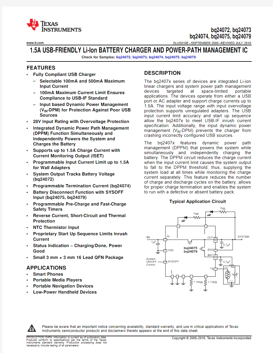
Typical Application Circuit ?Programmable Pre-Charge and Fast-Charge
Safety Timers
?Reverse Current,Short-Circuit and Thermal
Protection
?NTC Thermistor Input
?Proprietary Start Up Sequence Limits Inrush
Current
?Status Indication–Charging/Done,Power
Good
?Small3mm×3mm16Lead QFN Package
APPLICATIONS
?Smart Phones
?Portable Media Players
?Portable Navigation Devices
?Low-Power Handheld Devices
Please be aware that an important notice concerning availability,standard warranty,and use in critical applications of Texas
Instruments semiconductor products and disclaimers thereto appears at the end of this data sheet.
Copyright?2008–2010,Texas Instruments Incorporated Products conform to specifications per the terms of the Texas
bq24072,bq24073
bq24074,bq24075,bq24079
SLUS810E–SEPTEMBER2008–REVISED https://www.doczj.com/doc/2d10872499.html, This integrated circuit can be damaged by ESD.Texas Instruments recommends that all integrated circuits be handled with appropriate precautions.Failure to observe proper handling and installation procedures can cause damage.
ESD damage can range from subtle performance degradation to complete device failure.Precision integrated circuits may be more susceptible to damage because very small parametric changes could cause the device not to meet its published specifications.
DESCRIPTION(CONTINUED)
Additionally,the regulated system input enables instant system turn-on when plugged in even with a totally discharged battery.The power-path management architecture also permits the battery to supplement the system current requirements when the adapter cannot deliver the peak system currents,enabling the use of a smaller adapter.
The battery is charged in three phases:conditioning,constant current,and constant voltage.In all charge phases,an internal control loop monitors the IC junction temperature and reduces the charge current if the internal temperature threshold is exceeded.The charger power stage and charge current sense functions are fully integrated.The charger function has high accuracy current and voltage regulation loops,charge status display,and charge termination.The input current limit and charge current are programmable using external resistors.
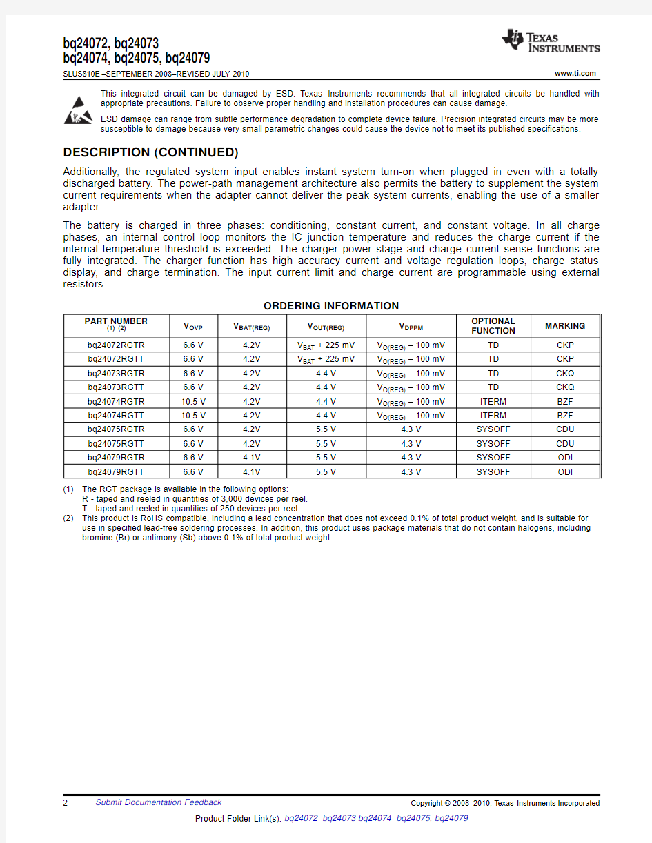
ORDERING INFORMATION
PART NUMBER OPTIONAL
V OVP V BAT(REG)V OUT(REG)V DPPM MARKING
(1)(2)FUNCTION
bq24072RGTR 6.6V 4.2V V BAT+225mV V O(REG)–100mV TD CKP bq24072RGTT 6.6V 4.2V V BAT+225mV V O(REG)–100mV TD CKP bq24073RGTR 6.6V 4.2V 4.4V V O(REG)–100mV TD CKQ bq24073RGTT 6.6V 4.2V 4.4V V O(REG)–100mV TD CKQ bq24074RGTR10.5V 4.2V 4.4V V O(REG)–100mV ITERM BZF bq24074RGTT10.5V 4.2V 4.4V V O(REG)–100mV ITERM BZF bq24075RGTR 6.6V 4.2V 5.5V 4.3V SYSOFF CDU bq24075RGTT 6.6V 4.2V 5.5V 4.3V SYSOFF CDU bq24079RGTR 6.6V 4.1V 5.5V 4.3V SYSOFF ODI bq24079RGTT 6.6V 4.1V 5.5V 4.3V SYSOFF ODI
(1)The RGT package is available in the following options:
R-taped and reeled in quantities of3,000devices per reel.
T-taped and reeled in quantities of250devices per reel.
(2)This product is RoHS compatible,including a lead concentration that does not exceed0.1%of total product weight,and is suitable for
use in specified lead-free soldering processes.In addition,this product uses package materials that do not contain halogens,including bromine(Br)or antimony(Sb)above0.1%of total product weight.
2Submit Documentation Feedback Copyright?2008–2010,Texas Instruments Incorporated
bq24072,bq24073
bq24074,bq24075,bq24079 https://www.doczj.com/doc/2d10872499.html, SLUS810E–SEPTEMBER2008–REVISED JULY2010 ABSOLUTE MAXIMUM RATINGS(1)
over the0°C to125°C operating free-air temperature range(unless otherwise noted)
VALUE UNIT
IN(with respect to VSS)–0.3to28V
BAT(with respect to VSS)–0.3to5V
V I Input Voltage
OUT,EN1,EN2,CE,TS,ISET,PGOOD,CHG,ILIM,TMR,ITERM,
–0.3to7V
SYSOFF,TD(with respect to VSS)
I I Input Current IN 1.6A
OUT5A Output Current
I O BAT(Discharge mode)5A
(Continuous)
BAT(Charging mode) 1.5(2)A Output Sink Current CHG,PGOOD15mA
T J Junction temperature–40to150°C
T stg Storage temperature–65to150°C (1)Stresses beyond those listed under absolute maximum ratings may cause permanent damage to the device.These are stress ratings
only,and functional operation of the device at these or any other conditions beyond those indicated under recommended operating conditions is not implied.Exposure to absolute-maximum-rated conditions for extended periods may affect device reliability.All voltage values are with respect to the network ground terminal unless otherwise noted.
(2)The IC operational charging life is reduced to20,000hours,when charging at1.5A and125°C.The thermal regulation feature reduces
charge current if the IC’s junction temperature reaches125°C;thus without a good thermal design the maximum programmed charge current may not be reached.
DISSIPATION RATINGS
POWER RATING PACKAGE(1)R q JA R q JC
T A≤25°C T A=85°C RGT(2)39.47°C/W 2.4°C/W 2.3W225mW
(1)For the most current package and ordering information,see the Package Option Addendum at the end of this document,or see the TI
website at https://www.doczj.com/doc/2d10872499.html,.
(2)This data is based on using the JEDEC High-K board and the exposed die pad is connected to a Cu pad on the board.The pad is
connected to the ground plane by a2x3via matrix.
RECOMMENDED OPERATING CONDITIONS
MIN MAX UNIT IN voltage range 4.3526V
V I’72,’73,‘75,'79 4.35 6.4 IN operating voltage range V
‘74 4.3510.2
I IN Input current,IN pin 1.5A
I OUT Current,OUT pin 4.5A
I BAT Current,BAT pin(Discharging) 4.5A
I CHG Current,BAT pin(Charging) 1.5(1)A
T J Junction Temperature–40125°C
R ILIM Maximum input current programming resistor11008000?
R ISET Fast-charge current programming resistor(2)5903000?
R ITERM Termination current programming resistor015k?
R TMR Timer programming resistor1872k?(1)The IC operational charging life is reduced to20,000hours,when charging at1.5A and125°C.The thermal regulation feature reduces
charge current if the IC’s junction temperature reaches125°C;thus without a good thermal design the maximum programmed charge current may not be reached.
(2)Use a1%tolerance resistor for R ISET to avoid issues with the R ISET short test when using the maximum charge current setting. Copyright?2008–2010,Texas Instruments Incorporated Submit Documentation Feedback3
bq24072,bq24073
bq24074,bq24075,bq24079
SLUS810E–SEPTEMBER2008–REVISED https://www.doczj.com/doc/2d10872499.html, ELECTRICAL CHARACTERISTICS
Over junction temperature range(0°≤T J≤125°C)and the recommended supply voltage range(unless otherwise noted) PARAMETER TEST CONDITIONS MIN TYP MAX UNIT INPUT
UVLO Undervoltage lock-out V IN:0V→4V 3.2 3.3 3.4V
V hys Hysteresis on UVLO V IN:4V→0V200300mV
Input power detected when V IN>V BAT+V IN(DT)
V IN(DT)Input power detection threshold5580130mV
V BAT=3.6V,VIN:3.5V→4V
V hys Hysteresis on V IN(DT)V BAT=3.6V,V IN:4V→3.5V20mV
Time measured from V IN:0V→5V1m s
t DGL(PGOOD)Deglitch time,input power detected status 1.2ms
rise-time to PGOOD=LO
V IN:5V→7V(’72,’73,’75,'79) 6.4 6.6 6.8
V OVP Input overvoltage protection threshold V
V IN:5V→11V(’74)10.210.510.8
V IN:7V→5V(’72,’73,’75,'79)110
V hys Hysteresis on OVP mV
V IN:11V→5V(’74)175
t DGL(OVP)Input overvoltage blanking time(OVP fault deglitch)50m s
Time measured from V IN:11V→5V with1m s
t REC Input overvoltage recovery time 1.2ms
fall-time to PGOOD=LO
ILIM,ISET SHORT CIRCUIT DETECTION(CHECKED DURING STARTUP)
I SC Current source V IN>UVLO and V IN>V BAT+V IN(DT) 1.3mA
V SC V IN>UVLO and V IN>V BAT+V IN(DT)520mV QUIESCENT CURRENT
CE=LO or HI,input power not detected,
I BAT(PDWN)Sleep current into BAT pin 6.5m A
No load on OUT pin,T J=85°C
EN1=HI,EN2=HI,V IN=6V,T J=85°C50
I IN Standby current into IN pin m A
EN1=HI,EN2=HI,V IN=10V,T J=85°C200
CE=LO,V IN=6V,no load on OUT pin,
I CC Active supply current,IN pin 1.5mA
V BAT>V BAT(REG),(EN1,EN2)≠(HI,HI)
POWER PATH
V DO(IN-OUT)V IN–V OUT V IN=4.3V,I IN=1A,V BAT=4.2V300475mV
V DO(BAT-OUT)V BAT–V OUT I OUT=1A,V IN=0V,V BAT>3V50100mV
V IN>V OUT+V DO(IN-OUT),V BAT<3.2V 3.3 3.4 3.5
OUT pin voltage regulation(bq24072)V
BAT +V BAT+V BAT+
V IN>V OUT+V DO(IN-OUT),V BAT≥3.2V
150mV225mV270mV
V O(REG)V OUT pin voltage regulation(bq24073,bq24074)V IN>V OUT+V DO(IN-OUT) 4.3 4.4 4.5
OUT pin voltage regulation(bq24075,bq24079)V IN>V OUT+V DO(IN-OUT) 5.4 5.5 5.6
EN1=LO,EN2=LO9095100
mA
I IN max Maximum input current EN1=HI,EN2=LO450475500
EN2=HI,EN1=LO K ILIM/R ILIM A
I LIM=500mA to1.5A150016101720
K ILIM Maximum input current factor A?
I LIM=200mA to500mA133015251720
I IN max Programmable input current limit range EN2=HI,EN1=LO,R ILIM=8k?to1.1k?2001500mA
Input voltage threshold when input current is
V IN-DPM EN2=LO,EN1=X 4.35 4.5 4.63V reduced
V O(REG)–V O(REG)–V O(REG)–
(’72,’73,’74)V Output voltage threshold when charging current is180mV100mV30mV
V DPPM
reduced
(’75,'79) 4.2 4.3 4.4V
V OUT≤V BAT
V BSUP1Enter battery supplement mode V BAT=3.6V,R ILIM=1.5k?,R LOAD=10?→2?V
–40mV
V OUT≥
V BSUP2Exit battery supplement mode V BAT=3.6V,R ILIM=1.5k?,R LOAD=2?→10?V
V BAT–20mV
V O(SC1)Output short-circuit detection threshold,power-on V IN>V UVLO and V IN>V BAT+V IN(DT)0.80.91V
Output short-circuit detection threshold,supplement
V O(SC2)V IN>V UVLO and V IN>V BAT+V IN(DT)200250300mV mode V BAT–V OUT>V O(SC2)indicates short-circuit
t DGL(SC2)Deglitch time,supplement mode short circuit250m s
t REC(SC2)Recovery time,supplement mode short circuit60ms
4Submit Documentation Feedback Copyright?2008–2010,Texas Instruments Incorporated
bq24072,bq24073
bq24074,bq24075,bq24079 https://www.doczj.com/doc/2d10872499.html, SLUS810E–SEPTEMBER2008–REVISED JULY2010 ELECTRICAL CHARACTERISTICS(continued)
Over junction temperature range(0°≤T J≤125°C)and the recommended supply voltage range(unless otherwise noted) PARAMETER TEST CONDITIONS MIN TYP MAX UNIT BATTERY CHARGER
I BAT Source current for BAT pin short-circuit detection V BAT=1.5V47.511mA
V BAT(SC)BAT pin short-circuit detection threshold V BAT rising 1.6 1.82V
('72,'73,'74,'75) 4.16 4.20 4.23
V BAT(REG)Battery charge voltage V
('79) 4.059 4.100 4.141
V LOWV Pre-charge to fast-charge transition threshold V IN>V UVLO and V IN>V BAT+V IN(DT) 2.93 3.1V
t DGL1(LOWV)Deglitch time on pre-charge to fast-charge transition25ms
t DGL2(LOWV)Deglitch time on fast-charge to pre-charge transition25ms
V BAT(REG)>V BAT>V LOWV,V IN=5V CE=LO,
Battery fast charge current range3001500mA
EN1=LO,EN2=HI
I CHG CE=LO,EN1=LO,EN2=HI,
Battery fast charge current V BAT>V LOWV,V IN=5V,I IN max>I CHG,no load on OUT pin,K ISET/R ISET A
thermal loop and DPPM loop not active
K ISET Fast charge current factor797890975A?
I PRECHG Pre-charge current K PRECHG/R ISET A
K PRECHG Pre-charge current factor7088106A?
CE=LO,(EN1,EN2)≠(LO,LO),
0.09×I CHG0.1×I CHG0.11×I CHG
V BAT>V RCH,t loop not active Termination comparator detection threshold I TERM A (internally set)CE=LO,(EN1,EN2)=(LO,LO), 0.027×I CHG0.033×I CHG0.040×I CHG V BAT>V RCH,t loop not active I BIAS(ITERM)Current for external termination-setting resistor V IN>V UVLO and V IN>V BAT+V IN(DT)727578m A Termination current threshold(externally set) I TERM K ITERM×R ITERM/R ISET A (bq24074) USB500or ISET mode(EN1,EN2)≠(LO,LO) 0.02250.03000.0375 CE=LO,V BAT>V RCH,t thermal loop not active K Factor for termination detection threshold K ITERM A (externally set)(bq24074)USB100mode(EN1,EN2)=(LO,LO), 0.0080.01000.012 CE=LO,V BAT>V RCH,t thermal loop not active t DGL(TERM)Deglitch time,termination detected25ms V BAT(REG)V BAT(REG)V BAT(REG) V RCH Recharge detection threshold V IN>V UVLO and V IN>V BAT+V IN(DT)V –140mV–100mV–60mV t DGL(RCH)Deglitch time,recharge threshold detected62.5ms V BAT=3.6V.Time measured from t DGL(NO-IN)Delay time,input power loss to OUT LDO turn-off20ms V IN:5V→3V1m s fall-time I BAT(DET)Sink current for battery detection V BAT=2.5V57.510mA t DET Battery detection timer BAT high or low250ms BATTERY CHARGING TIMERS t PRECHG Pre-charge safety timer value TMR=floating144018002160s t MAXCHG Charge safety timer value TMR=floating144001800021600s t PRECHG Pre-charge safety timer value18k? t MAXCHG Charge safety timer value18k? K TMR Timer factor364860s/k?BATTERY-PACK NTC MONITOR(1) I NTC NTC bias current V IN>UVLO and V IN>V BAT+V IN(DT)727578m A V HOT High temperature trip point Battery charging,V TS Falling270300330mV V HYS(HOT)Hysteresis on high trip point Battery charging,V TS Rising from V HOT30mV V COLD Low temperature trip point Battery charging,V TS Rising200021002200mV V HYS(COLD)Hysteresis on low trip point Battery charging,V TS Falling from V COLD300mV t DGL(TS)Deglitch time,pack temperature fault detection TS fault detected to charger disable50ms V DIS(TS)TS function disable threshold(bq24072,bq24073)TS unconnected V IN-200mV V THERMAL REGULATION T J(REG)Temperature regulation limit125°C T J(OFF)Thermal shutdown temperature T J Rising155°C T J(OFF-HYS)Thermal shutdown hysteresis20°C (1)These numbers set trip points of0°C and50°C while charging,with3°C hysteresis on the trip points,with a Vishay Type2curve NTC with an R25of10k?. Copyright?2008–2010,Texas Instruments Incorporated Submit Documentation Feedback5 E T R E T E R M R S O F F E T R bq24072,bq24073 bq24074,bq24075,bq24079 SLUS810E –SEPTEMBER 2008–REVISED JULY 2010 https://www.doczj.com/doc/2d10872499.html, ELECTRICAL CHARACTERISTICS (continued) Over junction temperature range (0°≤T J ≤125°C)and the recommended supply voltage range (unless otherwise noted) PARAMETER TEST CONDITIONS MIN TYP MAX UNIT LOGIC LEVELS ON EN1,EN2,CE,SYSOFF,TD V IL Logic LOW input voltage 00.4V V IH Logic HIGH input voltage 1.4 6V I IL Input sink current V IL =0V 1m A I IH Input source current V IH =1.4V 10 m A LOGIC LEVELS ON PGOOD,CHG V OL Output LOW voltage I SINK =5mA 0.4 V RGT PACKAGE (Top View) PIN FUNCTIONS PIN NO. I/O DESCRIPTION NAME '72,'73'74'75,'79External NTC Thermistor Input.Connect the TS input to the NTC thermistor in the battery pack.TS monitors TS 111I a 10k ?NTC thermistor.For applications that do not utilize the TS function,connect a 10k ?fixed resistor from TS to VSS to maintain a valid voltage level on TS. Charger Power Stage Output and Battery Voltage Sense Input.Connect BAT to the positive terminal of the BAT 2,3 2,3 2,3 I/O battery.Bypass BAT to VSS with a 4.7m F to 47m F ceramic capacitor. Charge Enable Active-Low Input.Connect CE to a high logic level to place the battery charger in standby mode.In standby mode,OUT is active and battery supplement mode is still available.Connect CE to a low CE 444I logic level to enable the battery charger.CE is internally pulled down with ~285k ?.Do not leave CE unconnected to ensure proper operation. EN2555I Input Current Limit Configuration https://www.doczj.com/doc/2d10872499.html,e EN1and EN2control the maximum input current and enable USB compliance.See Table 2for the description of the operation states.EN1and EN2are internally pulled EN1666I down with ?285k ?.Do not leave EN1or EN2unconnected to ensure proper operation. Open-drain Power Good Status Indication Output.PGOOD pulls to VSS when a valid input source is PGOOD 777O detected.PGOOD is high-impedance when the input power is not within specified limits.Connect PGOOD to the desired logic voltage rail using a 1k ?-100k ?resistor,or use with an LED for visual indication.VSS 888–Ground.Connect to the thermal pad and to the ground rail of the circuit. Open-Drain Charging Status Indication Output.CHG pulls to VSS when the battery is charging.CHG is high CHG 9 9 9 O impedance when charging is complete and when charger is disabled.Connect CHG to the desired logic voltage rail using a 1k ?-100k ?resistor,or use with an LED for visual indication. System Supply Output.OUT provides a regulated output when the input is below the OVP threshold and above the regulation voltage.When the input is out of the operation range,OUT is connected to V BAT except OUT 10,1110,1110,11O when SYSOFF is high (bq24075and bq24079only).Connect OUT to the system load.Bypass OUT to VSS with a 4.7m F to 47m F ceramic capacitor. Adjustable Current Limit Programming Input.Connect a 1100?to 8k ?resistor from ILIM to VSS to program ILIM 121212I the maximum input current (EN2=1,EN1=0).The input current includes the system load and the battery charge current.Leaving ILIM unconnected disables all charging. Input Power Connection.Connect IN to the external DC supply (AC adapter or USB port).The input operating range is 4.35V to 6.6V (bq24072,bq24073,bq24075,and bq24079)or 4.35V to 10.5V (bq23074).The input IN 131313I can accept voltages up to 26V without damage but operation is suspended.Connect bypass capacitor 1m F to 10m F to VSS.6Submit Documentation Feedback Copyright ?2008–2010,Texas Instruments Incorporated bq24072,bq24073 bq24074,bq24075,bq24079 https://www.doczj.com/doc/2d10872499.html, SLUS810E–SEPTEMBER2008–REVISED JULY2010 PIN FUNCTIONS(continued) PIN NO.I/O DESCRIPTION NAME '72,'73'74'75,'79 Timer Programming Input.TMR controls the pre-charge and fast-charge safety timers.Connect TMR to VSS TMR141414I to disable all safety timers.Connect a18k?to72k?resistor between TMR and VSS to program the timers a desired length.Leave TMR unconnected to set the timers to the default values. Termination Disable Input.Connect TD high to disable charger termination.Connect TD to VSS to enable charger termination.TD is checked during startup only and cannot be changed during operation.See the TD TD15––I section in this datasheet for a description of the behavior when termination is disabled.TD is internally pulled down to VSS with~285k?.Do not leave TD unconnected to ensure proper operation. Termination Current Programming Input.Connect a0?to15k?resistor from ITERM to VSS to program the ITERM–15–I termination current.Leave ITERM unconnected to set the termination current to the default10%termination threshold. System Enable Input.Connect SYSOFF high to turn off the FET connecting the battery to the system output. When an adapter is connected,charging is also disabled.Connect SYSOFF low for normal operation. SYSOFF––15I SYSOFF is internally pulled up to V BAT through a large resistor(~5M?).Do not leave SYSOFF unconnected to ensure proper operation. Fast Charge Current Programming Input.Connect a590?to3k?resistor from ISET to VSS to program the fast charge current level.Charging is disabled if ISET is left unconnected.While charging,the voltage at ISET ISET161616I/O reflects the actual charging current and can be used to monitor charge current.See the CHARGE CURRENT TRANSLATOR section for more details. There is an internal electrical connection between the exposed thermal pad and the VSS pin of the device. Thermal The thermal pad must be connected to the same potential as the VSS pin on the printed circuit board.Do not – Pad use the thermal pad as the primary ground input for the device.VSS pin must be connected to ground at all times. Table1.EN1/EN2Settings EN2EN1Maximum input current into IN pin https://www.doczj.com/doc/2d10872499.html,B100mode https://www.doczj.com/doc/2d10872499.html,B500mode 10Set by an external resistor from ILIM to VSS 11Standby(USB suspend mode) Copyright?2008–2010,Texas Instruments Incorporated Submit Documentation Feedback7 bq24072,bq24073 bq24074,bq24075,bq24079 SLUS810E–SEPTEMBER2008–REVISED https://www.doczj.com/doc/2d10872499.html, SIMPLIFIED BLOCK DIAGRAM Array 8Submit Documentation Feedback Copyright?2008–2010,Texas Instruments Incorporated V 500 mV/div 5 V/div I V 5 V/div V V 500 mA/div V CHG I BAT 2 V/div V BAT 1A/div 5 V/div 2 V/div 400ms/div A/div 5 V/div I I V 3.6 V BAT V 3.825 V OUT I OUT I BAT V 3.8 V BAT 500 mA/div 500 mV/div 1 ms/div V 4.4 V OUT 1A/div Supplement Mode I OUT I BAT 200 mV/div 400s/div m V 4.4 V OUT 500 mA/div 500 mA/div 5 V/div 2 V/div 400s/div m 500 mA/div V SYSOFF I BAT V 4 V BAT V 5.5 V OUT V CE I BAT V 3.6 V BAT V CHG 500 mA/div 1 V/div 5 V/div 5 V/div 10 V/div 500 mV/div 1A/div 40s/div m V IN I BAT V 4.2 V BAT V 4.4 V OUT bq24072,bq24073 bq24074,bq24075,bq24079 https://www.doczj.com/doc/2d10872499.html, SLUS810E –SEPTEMBER 2008–REVISED JULY 2010 TYPICAL CHARACTERISTICS V IN =6V,EN1=1,EN2=0,bq24073application circuit,T A =25°C,unless otherwise noted. ADAPTER PLUG-IN BATTERY CONNECTED BATTERY DETECTION BATTERY DETECTION R LOAD =10? BATTERY INSERTED BATTERY REMOVED Figure 1.Figure 2. Figure 3. ENTERING AND EXITING BATTERY ENTERING AND EXITING BATTERY SUPPLEMENT MODE SUPPLEMENT MODE ENTERING AND EXITING DPPM MODE R LOAD =25?TO 4.5? R LOAD =20?TO 4.5? R LOAD =20?to 9? bq24074 bq24072 Figure 4.Figure 5.Figure 6. SYSTEM ON/OFF WITH INPUT OVP FAULT CONNECTED V IN =6V to 15V V IN =6V CHARGER ON/OF USING CE R LOAD =10? bq24075,bq24079 Figure 7.Figure 8.Figure 9. Copyright ?2008–2010,Texas Instruments Incorporated Submit Documentation Feedback 9 600 400 100 Temperature -C o 300200 5000 120125 130135140145 I - m A B A T 5 V/div 4 ms/div V I V V 255075 100T - Junction Temperature - °C J D r o p o u t V o l t a g e - V -V I N O U T 25 T - Junction Temperature - °C J D r o p o u t V o l t a g e - V -V B A T O U T 2.5 3 3.54 4.5 V - O u t p u t V o l t a g e - V O V - Battery Voltage - V BAT 0 25 50 75 100 125 T - Junction Temperature - °C J V - O u t p u t V o l t a g e - V O bq24072,bq24073 bq24074,bq24075,bq24079 SLUS810E –SEPTEMBER 2008–REVISED JULY 2010 https://www.doczj.com/doc/2d10872499.html, TYPICAL CHARACTERISTICS (continued) V IN =6V,EN1=1,EN2=0,bq24073application circuit,T A =25°C,unless otherwise noted. SYSTEM ON/OFF WITH INPUT NOT CONNECTED DROPOUT VOLTAGE V IN =0V vs bq24075,bq24079 THERMAL REGULATION TEMPERATURE Figure 10.Figure 11. Figure 12. DROPOUT VOLTAGE bq24072 bq24072 vs OUTPUT REGULATION VOLTAGE OUTPUT REGULATION VOLTAGE TEMPERATURE vs vs NO INPUT SUPPLY BATTERY VOLTAGE TEMPERATURE Figure 13.Figure 14.Figure 15. 10Submit Documentation Feedback Copyright ?2008–2010,Texas Instruments Incorporated 255075100125 T - Junction Temperature - °C J V - O u t p u t V o l t a g e - V O 4.30 4.334.35 4.384.40 4.434.45 25 50 75 100 125 T - Junction Temperature - °C J V - O u t p u t V o l t a g e - V O 4.180 4.185 4.1904.195 4.200 4.2054.210 51015202530 T - Junction Temperature - °C J V - R e g u l a t i o n V o l t a g e - V B A T 56 78910 V - Input Voltage - V I I - I n p u t C u r r e n t - m A L I M 0 255075100125T - Junction Temperature - °C J V - O u t p u t V o l t a g e T h r e s h o l d - V O V P 0 255075100125 T - Junction Temperature - °C J V - O u t p u t V o l t a g e T h r e s h o l d - V O V P bq24072,bq24073 bq24074,bq24075,bq24079 https://www.doczj.com/doc/2d10872499.html, SLUS810E –SEPTEMBER 2008–REVISED JULY 2010 TYPICAL CHARACTERISTICS (continued) V IN =6V,EN1=1,EN2=0,bq24073application circuit,T A =25°C,unless otherwise noted. bq24073/74 bq24075,bq24079 OUTPUT REGULATION VOLTAGE OUTPUT REGULATION VOLTAGE BAT REGULATION VOLTAGE vs vs vs TEMPERATURE TEMPERATURE TEMPERATURE Figure 16. Figure 17. Figure 18. bq24072/73/75/79 bq24074 bq24074 OVERVOLTAGE PROTECTION OVERVOLTAGE PROTECTION THRESHOLD THRESHOLD INPUT CURRENT LIMIT vs vs vs TEMPERATURE TEMPERATURE INPUT VOLTAGE Figure 19.Figure 20.Figure 21. Copyright ?2008–2010,Texas Instruments Incorporated Submit Documentation Feedback 11 3 3.2 3.4 3.6 3.84 4.2 I - F a s t C h a r g e C u r r e n t -A B A T V - Battery Voltage - V BAT 3 3.2 3.4 3.6 3.84 4.2 I - F a s t C h a r g e C u r r e n t -A B A T V - Battery Voltage - V BAT 95 96 979899100101102103104 1052 2.2 2.4 2.6 2.8 3 I - P r e c h a r g e C u r r e n t -A B A T V - Battery Voltage - V BAT 2 2.2 2.4 2.6 2.8 3 I - P r e c h a r g e C u r r e n t -A B A T V - Battery Voltage - V BAT bq24072,bq24073 bq24074,bq24075,bq24079 SLUS810E –SEPTEMBER 2008–REVISED JULY 2010 https://www.doczj.com/doc/2d10872499.html, TYPICAL CHARACTERISTICS (continued) V IN =6V,EN1=1,EN2=0,bq24073application circuit,T A =25°C,unless otherwise noted. FASTCHARGE CURRENT FASTCHARGE CURRENT PRECHARGE CURRENT vs vs vs BATTERY VOLTAGE BATTERY VOLTAGE BATTERY VOLTAGE Figure 22.Figure 23. Figure 24. PRECHARGE CURRENT vs BATTERY VOLTAGE Figure 25. 12Submit Documentation Feedback Copyright ?2008–2010,Texas Instruments Incorporated bq24072,bq24073 bq24074,bq24075,bq24079 https://www.doczj.com/doc/2d10872499.html, SLUS810E –SEPTEMBER 2008–REVISED JULY 2010 APPLICATION CIRCUITS V IN =UVLO to V OVP ,I FASTCHG =800mA,I IN(MAX)=1.3A,Battery Temperature Charge Range =0°C to 50°C,6.25hour Fastcharge Safety Timer Figure https://www.doczj.com/doc/2d10872499.html,ing bq24072/bq24073in a Host Controlled Charger Application Copyright ?2008–2010,Texas Instruments Incorporated Submit Documentation Feedback 13 bq24072,bq24073 bq24074,bq24075,bq24079 SLUS810E –SEPTEMBER 2008–REVISED JULY 2010 https://www.doczj.com/doc/2d10872499.html, V IN =UVLO to V OVP ,I FASTCHG =800mA,I IN(MAX)= 1.3A,I TERM =110mA,Battery Temperature Charge Range =0°C to 50°C,Safety Timers disabled Figure https://www.doczj.com/doc/2d10872499.html,ing bq24074in a Stand Alone Charger Application V IN =UVLO to V OVP ,I FASTCHG =800mA,I IN(MAX)=1.3A,Battery Temperature Charge Range =0°C to 50°C,6.25hour Fastcharge Safety Timer Figure https://www.doczj.com/doc/2d10872499.html,ing bq24075or bq24079to Disconnect the Battery from the System 14 Submit Documentation Feedback Copyright ?2008–2010,Texas Instruments Incorporated V OVP V BAT V + V - V BAT IN(DT)UVLO - V V I I V bq24072,bq24073 bq24074,bq24075,bq24079 https://www.doczj.com/doc/2d10872499.html, SLUS810E –SEPTEMBER 2008–REVISED JULY 2010 EXPLANATION OF DEGLITCH TIMES AND COMPARATOR HYSTERESIS Figures not to scale Figure 29.Power-Up,Power-Down,Power Good Indication Figure 30.Pre-to Fast-Charge,Fast-to Pre-Charge Transition –t DGL1(LOWV),t DGL2(LOWV) Figure 31.Recharge –t DGL(RCH) Copyright ?2008–2010,Texas Instruments Incorporated Submit Documentation Feedback 15 V V V - V COLD V - V HOT V bq24072,bq24073 bq24074,bq24075,bq24079 SLUS810E –SEPTEMBER 2008–REVISED JULY 2010 https://www.doczj.com/doc/2d10872499.html, Figure 32.OUT Short-Circuit –Supplement Mode Figure 33.Battery Pack Temperature Sensing –TS Pin.Battery Temperature Increasing 16Submit Documentation Feedback Copyright ?2008–2010,Texas Instruments Incorporated bq24072,bq24073 bq24074,bq24075,bq24079 https://www.doczj.com/doc/2d10872499.html, SLUS810E–SEPTEMBER2008–REVISED JULY2010 DETAILED FUNCTIONAL DESCRIPTION The bq2407x devices are integrated Li-Ion linear chargers and system power path management devices targeted at space-limited portable applications.The device powers the system while simultaneously and independently charging the battery.This feature reduces the number of charge and discharge cycles on the battery,allows for proper charge termination and enables the system to run with a defective or absent battery pack.It also allows instant system turn-on even with a totally discharged battery.The input power source for charging the battery and running the system can be an AC adapter or a USB port.The devices feature Dynamic Power Path Management(DPPM),which shares the source current between the system and battery charging,and automatically reduces the charging current if the system load increases.When charging from a USB port,the input dynamic power management(V IN-DPM)circuit reduces the input current if the input voltage falls below a threshold,preventing the USB port from crashing.The power-path architecture also permits the battery to supplement the system current requirements when the adapter cannot deliver the peak system currents. UNDERVOLTAGE LOCKOUT(UVLO) The bq2407X family remains in power down mode when the input voltage at the IN pin is below the undervoltage threshold(UVLO). During the power down mode the host commands at the control inputs(CE,EN1and EN2)are ignored.The Q1 FET connected between IN and OUT pins is off,and the status outputs CHG and PGOOD are high impedance. The Q2FET that connects BAT to OUT is ON.(If SYSOFF is high,Q2is off).During power down mode,the V OUT(SC2)circuitry is active and monitors for overload conditions on OUT. POWER ON When V IN exceeds the UVLO threshold,the bq2407x powers up.While V IN is below V BAT+V IN(DT),the host commands at the control inputs(CE,EN1and EN2)are ignored.The Q1FET connected between IN and OUT pins is off,and the status outputs and are high impedance.The Q2FET that connects BAT to OUT is ON.(If SYSOFF is high,Q2is off).During this mode,the V OUT(SC2)circuitry is active and monitors for overload conditions on OUT. Once V IN rises above V BAT+V IN(DT),PGOOD is driven low to indicate the valid power status and the CE,EN1, and EN2inputs are read.The device enters standby mode if(EN1=EN2=HI)or if an input overvoltage condition occurs.In standby mode,Q1is OFF and Q2is ON so OUT is connected to the battery input.(If SYSOFF is high,FET Q2is off).During this mode,the V OUT(SC2)circuitry is active and monitors for overload conditions on OUT. When the input voltage at IN is within the valid range:V IN>UVLO AND V IN>V BAT+V IN(DT)AND V IN Copyright?2008–2010,Texas Instruments Incorporated Submit Documentation Feedback17 bq24072,bq24073 bq24074,bq24075,bq24079 SLUS810E–SEPTEMBER2008–REVISED https://www.doczj.com/doc/2d10872499.html, Array Figure34.Startup Flow Diagram 18Submit Documentation Feedback Copyright?2008–2010,Texas Instruments Incorporated 100μs/div 20 m A /d i v U S B 100 C u r r e n t L i m i t bq24072,bq24073 bq24074,bq24075,bq24079 https://www.doczj.com/doc/2d10872499.html, SLUS810E –SEPTEMBER 2008–REVISED JULY 2010 OVERVOLTAGE PROTECTION (OVP) The bq2407x accepts inputs up to 28V without damage.Additionally,an overvoltage protection (OVP)circuit is implemented that shuts off the internal LDO and discontinues charging when V IN >V OVP for a period long than t DGL(OVP).When in OVP,the system output (OUT)is connected to the battery and is high impedance.Once the OVP condition is removed,a new power on sequence starts (See the POWER ON section).The safety timers are reset and a new charge cycle will be indicated by the output. DYNAMIC POWER-PATH MANAGEMENT The bq2407x features an OUT output that powers the external load connected to the battery.This output is active whenever a source is connected to IN or BAT.The following sections discuss the behavior of OUT with a source connected to IN to charge the battery and a battery source only.INPUT SOURCE CONNECTED (ADAPTER or USB) With a source connected,the dynamic power-path management (DPPM)circuitry of the bq2407x monitors the input current continuously.The OUT output for the bq24073/74/75/79is regulated to a fixed voltage (V O(REG)).For the bq24072,OUT is regulated to 200mV above the voltage at BAT.When the BAT voltage falls below 3.2V,OUT is clamped to 3.4V.This allows for proper startup of the system load even with a discharged battery.The current into IN is shared between charging the battery and powering the system load at OUT.The bq2407x has internal selectable current limits of 100mA (USB100)and 500mA (USB500)for charging from USB ports,as well as a resistor-programmable input current limit. The bq2407x is USB IF compliant for the inrush current testing.The USB spec allows up to 10m F to be hard started,which establishes 50m C as the maximum inrush charge value when exceeding 100mA.The input current limit for the bq2407x prevents the input current from exceeding this limit,even with system capacitances greater than 10m F.Note that the input capacitance to the device must be selected small enough to prevent a violation (<10m F),as this current is not limited.Figure 35demonstrates the startup of the bq2407x and compares it to the USB-IF specification. Figure https://www.doczj.com/doc/2d10872499.html,B-IF Inrush Current Test The input current limit selection is controlled by the state of the EN1and EN2pins as shown in Table 1.When using the resistor-programmable current limit,the input current limit is set by the value of the resistor connected from the ILIM pin to VSS,and is given by the equation: I IN-MAX =K ILIM /R ILIM (1) The input current limit is adjustable up to 1.5A.The valid resistor range is 1.1k ?to 8k ?. When the IN source is connected,priority is given to the system load.The DPPM and Battery Supplement modes are used to maintain the system load.Figure 37and Figure 38illustrate examples of the DPPM and supplement modes.These modes are explained in detail in the following sections. Copyright ?2008–2010,Texas Instruments Incorporated Submit Documentation Feedback 19 4 ms/div 500mV/div USB5Current Limit 00200mA/div 200mA/div 200mA/div I OUT I IN V IN (5V) I BAT Input collapses Input current limit is reduced to prevent crashing the supply Input regulated to V IN_DPM bq24072,bq24073 bq24074,bq24075,bq24079 SLUS810E –SEPTEMBER 2008–REVISED JULY 2010 https://www.doczj.com/doc/2d10872499.html, Input DPM Mode (V IN -DPM) The bq2407x utilizes the V IN -DPM mode for operation from current-limited USB ports.When EN1and EN2are configured for USB100(EN2=0,EN1=0)or USB500(EN2=0,EN2=1)modes,the input voltage is monitored.If V IN falls to V IN-DPM ,the input current limit is reduced to prevent the input voltage from falling further.This prevents the bq2407x from crashing poorly designed or incorrectly configured USB sources.Figure 36shows the V IN -DPM behavior to a current limited source.In this figure,the input source has a 400mA current limit and the device is in USB500mode (EN1=1,EN2=0). Figure 36.V IN -DPM Waveform DPPM Mode When the sum of the charging and system load currents exceeds the maximum input current (programmed with EN1,EN2and ILIM pins),the voltage at OUT decreases.Once the voltage on the OUT pin falls to V DPPM ,the bq2407x enters DPPM mode.In this mode,the charging current is reduced as the OUT current increases in order to maintain the system output.Battery termination is disabled while in DPPM mode.Battery Supplement Mode While in DPPM mode,if the charging current falls to zero and the system load current increases beyond the programmed input current limit,the voltage at OUT reduces further.When the OUT voltage drops below the V BSUP1threshold,the battery supplements the system load.The battery stops supplementing the system load when the voltage at OUT rises above the V BSUP2threshold. During supplement mode,the battery supplement current is not regulated (BAT-FET is fully on),however there is a short circuit protection circuit built in.Figure 5demonstrates supplement mode.If during battery supplement mode,the voltage at OUT drops V O(SC2)below the BAT voltage,the OUT output is turned off if the overload exists after t DGL(SC2).The short circuit recovery timer then starts counting.After t REC(SC2),OUT turns on and attempts to restart.If the short circuit remains,OUT is turned off and the counter restarts.Battery termination is disabled while in supplement mode. 20Submit Documentation Feedback Copyright ?2008–2010,Texas Instruments Incorporated bq24072,bq24073 bq24074,bq24075,bq24079 https://www.doczj.com/doc/2d10872499.html, SLUS810E–SEPTEMBER2008–REVISED JULY2010 1.5A USB-FRIENDLY Li-Ion BATTERY CHARGER AND POWER-PATH MANAGEMENT IC Check for Samples:bq24072,bq24073,bq24074,bq24075,bq24079 FEATURES DESCRIPTION ?Fully Compliant USB Charger –Selectable100mA and500mA Maximum The bq2407x series of devices are integrated Li-ion linear chargers and system power path management Input Current devices targeted at space-limited portable –100mA Maximum Current Limit Ensures applications.The devices operate from either a USB Compliance to USB-IF Standard port or AC adapter and support charge currents up to –Input based Dynamic Power Management 1.5A.The input voltage range with input overvoltage (V IN-DPM)for Protection Against Poor USB protection supports unregulated adapters.The USB Sources input current limit accuracy and start up sequence allow the bq2407x to meet USB-IF inrush current ?28V Input Rating with Overvoltage Protection specification.Additionally,the input dynamic power ?Integrated Dynamic Power Path Management management(V IN -DPM)prevents the charger from (DPPM)Function Simultaneously and crashing incorrectly configured USB sources. Independently Powers the System and The bq2407x features dynamic power path Charges the Battery management(DPPM)that powers the system while ?Supports up to1.5A Charge Current with simultaneously and independently charging the Current Monitoring Output(ISET)battery.The DPPM circuit reduces the charge current when the input current limit causes the system output ?Programmable Input Current Limit up to1.5A to fall to the DPPM threshold;thus,supplying the for Wall Adapters system load at all times while monitoring the charge ?System Output Tracks Battery Voltage current separately.This feature reduces the number (bq24072) of charge and discharge cycles on the battery,allows ?Programmable Termination Current(bq24074)for proper charge termination and enables the system to run with a defective or absent battery pack.?Battery Disconnect Function with SYSOFF Input(bq24075,bq24079) Typical Application Circuit ?Programmable Pre-Charge and Fast-Charge Safety Timers ?Reverse Current,Short-Circuit and Thermal Protection ?NTC Thermistor Input ?Proprietary Start Up Sequence Limits Inrush Current ?Status Indication–Charging/Done,Power Good ?Small3mm×3mm16Lead QFN Package APPLICATIONS ?Smart Phones ?Portable Media Players ?Portable Navigation Devices ?Low-Power Handheld Devices Please be aware that an important notice concerning availability,standard warranty,and use in critical applications of Texas Instruments semiconductor products and disclaimers thereto appears at the end of this data sheet. Copyright?2008–2010,Texas Instruments Incorporated Products conform to specifications per the terms of the Texas 随着手持设备业务的不断发展,对电池充电器的要求也不断增加。要为完成这项工作而选择正确的集成电路 (IC),我们必须权衡几个因素。在开始设计以前,我们必须考虑诸如解决方案尺寸、USB标准、充电速率和成本等因素。必须将这些因素按照重要程度依次排列,然后选择相应的充电器IC。本文中,我们将介绍不同的充电拓扑结构,并研究电池充电器IC的一些特性。此外,我们还将探讨一个应用和现有的解决方案。 锂离子电池充电周期 锂离子电池要求专门的充电周期,以实现安全充电并最大化电池使用时间。电池充电分两个阶段:恒定电流 (CC) 和恒定电压 (CV)。电池位于完全充满电压以下时,电流经过稳压进入电池。在CC模式下,电流经过稳压达到两个值之一。如果电池电压非常低,则充电电流降低至预充电电平,以适应电池并防止电池损坏。该阈值因电池化学属性而不同,一般取决于电池制造厂商。一旦电池电压升至预充电阈值以上,充电便升至快速充电电流电平。典型电池的最大建议快速充电电流为1C(C=1 小时内耗尽电池所需的电流),但该电流也取决地电池制造厂商。典型充电电流为~0.8C,目的是最大化电池使用时间。对电池充电时,电压上升。一旦电池电压升至稳压电压(一般为4.2V),充电电流逐渐减少,同时对电池电压进行稳压以防止过充电。在这种模式下,电池充电时电流逐渐减少,同时电池阻抗降低。如果电流降至预定电平(一般为快速充电电流的10%),则终止充电。我们一般不对电池浮充电,因为这样会缩短电池使用寿命。图1 以图形方式说明了典型的充电周期。 线性解决方案与开关模式解决方案对比 将适配器电压转降为电池电压并控制不同充电阶段的拓扑结构有两种:线性稳压器和电感开关。这两种拓扑结构在体积、效率、解决方案成本和电磁干扰(EMI) 辐射方面各有优缺点。我们下面介绍这两种拓扑结构的各种优点和一些折中方法。 一般来说,电感开关是获得最高效率的最佳选择。利用电阻器等检测组件,在输出端检测充电电流。充电器在CC 模式下时,电流反馈电路控制占空比。电池电压检测反馈电路控制CV 模式下的占空比。根据特性集的不同,可能会出现其他一些控制环路。我们将在后面详细讨论这些环路。电感开关电路要求开关组件、整流器、电感和输入及输出电容器。就许多应用而言,通过选择一种将开关 航天锂电池电源管理设计 随着人类科技的发展,航天已经成为当今世界最具挑战性的高科技领域之一。当前,电子器件产品的更新换代仍然跟随摩尔定律高速发展,飞行器的功能、性能不断多样化的同时,向航天电源产品提出了更高的要求,其中包括更大的能源储备、更强的瞬时功率输出、更长的使用时间。目前,第一代储能电池以镉镍蓄电池及镍氢电池作为航天电源中储能产品,而随着飞行器用电需求的增加,放电深度的不断增加,严重影响了电池产品的使用寿命。因此,我们开始寻求新的储能电池,在此大环境中,第二代电池产品锂电池开始进入航天电源产品,逐渐替代第一代电池产品作为航天器的电源储能产品,解决了航天电源中的能源短板,使得飞行器能具有更多的发展空间。 1.1航天电池 由于航天器需求的高速发展,要求储能电源具有很高的性能,即具有高能量密度、高功率密度、长寿命、宽工作温度范围、高安全性与可靠性等特征,现有的第一代电池很难在性能上取得更多的突破,而新一代储能电源锂离子电池相较于第一代储能电池相比,锂离子电池具有如下特点: (1)单体电池工作电压高达3.7V,是镉镍电池的3倍,镍氢电池的3倍; (2)比能量大,最高可达150Wh/Kg,镍氢电池的2倍。 (3)体积小,能量密度高,可达到400Wh/L。 (4)循环寿命长,循环次数可达1000次以上,在均衡充放电的情况下,使用年限可达5~10年,寿命约为镉镍电池的2倍。 (5)自放电率低。 (6)无记忆效应,可以随时随地的进行充电,并且电池充放电深度对电池的寿命影响不大,可以全充全放。 2.航天器锂电池管理控制系统 2.1航天电池管理需求 根据卫星用电需求、轨道环境等要求对锂电池的串并联数进行设计,因此对多个串并联组合的锂电池均衡管理成为一个设计难题。电池管理系统主要负责控制电池组的充放电电流,电池组系统的基本功能主要有: (1)电池数据采集; (2)电池状态监控; (3)电池安全管理; (4)电池均衡管理; (5)通信功能; 因此,通过硬件对蓄电池数据进行采集后,由软件实现逻辑管理的方法在设计上能使得产品设计更为简化和可靠。 2.2航天电池均衡管理软件设计 2.2.1电池管理软件介绍 数据采集与均衡控制任务是电池管理系统中优先级最高的任务,也是系统中运行频率最高的任务,正确的数据采集是电池管理系统正常运行的前提和基础。由于电压、电流和温度的数据采样频率都不同,為了同时进行电压、电流和温度的采集,程序中设计了一个全局的计数器,每采样一次电流值该计数器的值加1,当计数值达到电压采样周期时进行一次电压采样,达到温度采样周期时进行一次温度采样。这里所指的达到采样周期指的是计数值满足采样周期的整数倍,例如对于周期为50us的电流采样和周期就为lms的电压采样,计数值取20的整数倍。通过采集所得单体电压、单体电流及电池块温度数据,对各单体SOC值进行计算,获得各单体SOC值,然后通过各单体SOC值进行比较处理,送出相应的控制信号控制均衡执行电路对各单体电池进行SOC均衡。 由于航天产品中对产品可靠性的要求,因此在管理系统中需要设置安全保护电路,通过对安全数据参数的判断,控制单体充放电回路,从而避免电池过充或过放,起到保护电池单体延长电池使用寿命的作 文件修(制)订履历一览表 序号版次《文件审批单》编号发布日期修(制)订说明拟制审核批准备注1 A0 2 序号部门/ 人员是否发放发放数量序号部门/ 人员是否发放发放数量 1 总裁 3 综合管理部 2 总工程师 4 财务部 5 销售部10 销售部 6 技术部11 技术中心 电 池 7 制造部12 制造部 pack 厂 8 采购部13 采购部 9 质量部14 质量部 文控员备注 1、目的 在锂电池日常储存运输中,需要相应的知识做储备,同时还需要小心谨慎。作为特别容易发生化学反应的金属,锂电池易延伸和燃烧,所以在包装、运输、储存时没有按规定处理的话,可能会导致严重的事故——燃烧和爆炸。为加强公司锂电池存储的安全管理,防止发生火灾爆炸事故造成人员伤亡及财产损失,特制订公司锂电池安全管理规程。 2、适用范围 本文件适用有限公司所有电池生产、存储现场。 3、职责 3.1 安环部职责 安环部负责制定、修改公司级锂电池安全管理规程并监督该管理规定的贯彻落实,将锂电池 组装及存储部位作为巡查工作重点,着重检查现场安全防护及消防设施配备和运行情况以及 现场安全措施的有效性,发现“三违”问题及时制止,现场安全及防护措施存在隐患及时上 报处理。 3.2 仓储部门职责 锂电池组装及存储部门负责制定仓储安全操作规程并根据部门情况制定相应规章制度,确保 所有员工接受培训,将锂电池的运输、存储作为现场安全管理的重要工作。 4、电池仓库管理基本要求: 4.1 因锂电池特性问题,高温及湿温会加速电池的自放电,建议不打开包装的电池应贮存在环境温度为-5℃~35℃,相对湿度不大于90%的清洁、干燥、通风的库房内,库房内不应含有腐蚀性气体。 4.2 湿度要求:有效控制仓库湿度,避免仓库长时间处于极端湿度(相对湿度高于90%)。 4.3 锂电池仓库应用砖墙实体相隔,库房必须采用封闭、防爆或其他相应的安全电气照明设备。 4.4 存放电池的地点,应配备品种数量充足的消防器材(二氧化碳、干粉灭火器,消防水龙,消防沙箱)并确保处于良好状态。有条件的情况下建议安装自动雨喷淋灭火系统。不能与易燃的物料(如包装材料纸盒、纸箱等)放在同一仓库,建议用独立的仓库。 4.5 有锂电池的地方,一定要有严禁吸烟等一些违禁条例规定。 摘要 锂离子电池的众多优点使其在小型便携设备中获得了广泛应用,但与镍铬、镍氢电池不同的是锂离子电池需要更安全高效的充电控制,并随着智能化程度的进一步发展,迫切需要一个高精度的锂电池监测电路以全面掌握电池状态,决定控制策略,从而提高系统运行可靠性。鉴于此,本文在分析锂离子电池充电技术的发展趋势和充电过程性能特点的基础上,提出了一种电源管理系统控制单元设计。这种控制单元主要由基于DS2741的监测电路、基于MAX1898的充电电路和基于AT89C51控制单元构成。本文具体的内容包括锂电池充电技术、充电电路设计以及监测电路设计等。最后总结了本次研究的工作目标,研究进展和发展前景。关键词:锂离子电池;电源管理;充电电路;监测电路 Abstract Numerous advantages of the lithium-ion battery make it acquire the extensive application in Small portable devices, but different from chrome of nickel , the nickel hydrogen battery is the lithium-ion battery to need the safety to refresh the control efficiently, and along with the further development that the intelligence turns the degree, need a lithium battery of high accuracy monitor electric circuit urgently to control the battery appearance completely, decide to control the strategy, thus raise the system movement credibility.Owing to this, this text on the basis of the analysis of lithium-ion battery charging technology trends and charging process performance , put forward a kind of power management system control unit design.The control unit by the monitoring circuit based on the DS2741, MAX1898-based charging circuit and control unit based on AT89C51 composition.the concrete contents include Li-ion battery charging technology, charging circuit design and testing of circuit design etc..Tallied up a work target for study finally, the research makes progress and development prospects. Keyword: The lithium-ion battery;Power Management;Refresh the electric circuit; 先进的锂电池线性充电管理芯片BQ2057及其应用 北京理工大学机电工程学院魏维伟李杰 摘要:本文介绍美国TI公司生产的先进锂电池充电管理芯片BQ2057,利用BQ2057系列芯片及简单外围电路可设计低成本的单/双节锂电池充电器,非常适用于便携式电子仪器的紧凑设计。本文将在介绍BQ2057芯片的特点、功能的基础上,给出典型充电电路的设计方法及应用该充电芯片设计便携式仪器的体会。 关键词:锂电池充电器BQ2057 1 引言 BQ2057系列是美国TI公司生产的先进锂电池充电管理芯片,BQ2057系列芯片适合单节(4.1V或4.2V)或双节(8.2V或8.4V)锂离子(Li-Ion)和锂聚合物(Li-Pol)电池的充电需要,同时根据不同的应用提供了MSOP、TSSOP和SOIC的可选封装形式,利用该芯片设计的充电器外围电路及其简单,非常适合便携式电子产品的紧凑设计需要。BQ2057可以动态补偿锂电池组的内阻以减少充电时间,带有可选的电池温度监测,利用电池组温度传感器连续检测电池温度,当电池温度超出设定范围时BQ2057关闭对电池充电。内部集成的恒压恒流器带有高/低边电流感测和可编程充电电流,充电状态识别可由输出的LED指示灯或与主控器接口实现,具有自动重新充电、最小电流终止充电、低功耗睡眠等特性。 2.功能及特性 2.1 器件封装及型号选择 BQ2057系列充电芯片为满足设计需要,提供了多种可选封装及型号,其封装形式如图2-1所示,有MSOP、TSSOP和SOIC三种封装形式。其型号如表2-1所示,有BQ2057、BQ2057C、BQ2057T和BQ2057W四种信号,分别适合4.1V、4.2V、8.2V和8.4V的充电需要。 元件型号充电电压 BQ2057 4.1V BQ2057C 4.2V BQ2057T 8.2V BQ2057W 8.4V BQ2057的引脚功能描述如下: ?VCC (引脚1):工作电源输入; ?TS (引脚2):温度感测输入,用于检测电池组的温度; ?STA T(引脚3):充电状态输出,包括:充电中、充电完成和温度故障三个状态; ?VSS (引脚4):工作电源地输入; ?CC (引脚5):充电控制输出; ?COMP(引脚6):充电速率补偿输入; ?SNS (引脚7):充电电流感测输入; ?BA T (引脚8):锂电池电压输入; 锂电池安全管理规程 一、目的 为加强公司锂电池组装及存储管理,防止发生火灾爆炸事故造成人员伤亡及财产损失,特制订公司锂电池安全管理规程。 二、使用范围 本管理规定适用于公司组装及存储锂电池的车间及仓库。 三、职责 1、安全科职责 综合管理部安全科负责制定、修改公司级锂电池安全管理规程并监督该管理规定的贯彻落实,将锂电池组装及存储部位作为巡查工作重点,着重检查现场安全防护及消防设施配备和运行情况以及现场安全措施的有效性,发现“三违”问题及时制止,现场安全及防护措施存在隐患及时上报处理。 2、生产部门 锂电池组装及存储部门负责制定安全生产操作规程(SOP)并根据部门情况制定相应规章制度,确保所有员工接受培训,将锂电池的生产、运输、存储作为现场安全管理的重要工作。 四、锂电池火灾危险性 1、锂电池火灾特性 锂电池能够自燃,随后会因为过热而发生爆炸。产生过热的原因包括电短路,快速放电,过度充电,制造缺陷,设计不良或机械损坏等等。过热会导致”热失控”过程的产生,也就是电池内部的放热反应会导致电池内部温度和压力以很快速率上升,从而将能量浪费掉。一旦某个电池单元进入热失控状态,它会产生足够的热量,使得相邻的电池单元也进入热失控状态。随着每个电池单元轮流破裂并释放其内含物,就会产生一种反复燃烧的火焰。这就造成电池中的可燃性电解液发生泄漏,如果使用一次性锂电池,则还会释放可燃烧的锂金属。于是就会产生一个巨大的问题,这些火灾不能像“正常”火灾一样对待,需要开展有针对性的培训,防控规划,合理存储和建立灭火系统等。 2、事故原因 存储运输时,电池机械损伤引发热失控; 电池组装过程中,收到挤压或刺破损坏; 锂电池因工艺或其他问题造成内部短路,造成迅速升温、过热自燃或爆炸; 锂电池对环境温度和湿度比较敏感,发生自燃; Tesla Model S电池组设计全面解析 对Tesla来说最近可谓是祸不单行:连续发生了3起起火事故,市值狂跌40亿,刚刚又有3名工人受伤送医。Elon Musk就一直忙着到处“灭火”,时而还跟公开表示对Tesla “不感冒”的乔治·克鲁尼隔空喊话。在经历了首次盈利、电池更换技术、穿越美国、水陆两栖车等头条新闻后,Elon Musk最近总以各种负面消息重返头条。这位“钢铁侠”CEO在2013年真是遭遇各种大起大落。 其中最为人关注的莫过于Model S的起火事故,而在起火事故中最核心的问题就是电池技术。可以说,牵动Tesla股价起起落落的核心元素就是它的电池技术,这是投资者最关心的问题。在美国发生的两起起火事故有着相似的情节:Model S撞击到金属物体后,导致电池起火,但火势都被很好地控制在车头部分。在墨西哥的事故中,主要的燃烧体也是电池。而且在3起事故中,如何把着火的电池扑灭对消防员来说都是个难题。 这让很多人产生一个疑问:Model S的电池就这么不禁撞吗?在之前的一篇文章中我跟大家简单讨论了一下这个问题,但只是停留在表面。读者现在都了解的是:Model S的电池位于车辆底部,采用的是松下提供的18650钴酸锂电池,整个电池组包含约8000块电池单元;钴酸锂电池能量密度大,但稳定性较差,为此Tesla研发了3级电源管理体系来确保电池组正常运作。现在,我们找到了Tesla的一份电池技术专利,借此来透彻地了解下Model S电池的结构设计和技术特征。 电池的布局与形体 如专利图所示,Model S的电池组位于车辆的底盘,与轮距同宽,长度略短于轴距。电池组的实际物理尺寸是:长2.7m,宽1.5m,厚度为0.1m至0.18m。其中0.18m较厚的部分是由于2个电池模块叠加造成的。这个物理尺寸指的是电池组整体的大小,包括上下、左右、前后的包裹面板。这个电池组的结构是一个通用设计,除了18650电池外,其他符合条件的电池也可以安装。此外,电池组采用密封设计,与空气隔绝,大部分用料为铝或铝合金。可以说,电池不仅是一个能源中心,同时也是Model S底盘的一部分,其坚固的外壳能对车辆起到很好的支撑作用。 由于与轮距等宽,电池组的两侧分别与车辆两侧的车门槛板对接,用螺丝固定。电池组的横断面低于车门槛板。从正面看,相当于车门槛板“挂着”电池组。其连接部分如下图所示。 电池内部结构 Model S电池组在内部被划分为7个区域(605),每个区域安装两个电池模块(701),每个模块内置370块电池单元。在电池组头部还有一个突出部分(607),其厚度也较高,这就是上文提到的0.18m的部分,安装了两个电池模块,堆叠排放。这样计算下来一共有5920块电池单元。同时这7个区域(包括突出部分一共是8个空间)相互之间是完全隔绝 锂电池仓库管理要求 由于锂是一种特别容易发生化学反应的金属,易延伸和燃烧,锂电池包装和运输,如处理不当,易燃烧和爆炸,事故也时有发生,因此特对锂电池仓库管理做如下要求: 一、基本要求: (1)锂电池及锂电池组属危险品;为保障后续搬运运输安全,所有锂电池(组)须通过UN38.3测试; (2)因锂电池特性问题,所以储存环境要在18-25度内。 (3)湿度要求:有效控制仓库湿度,避免仓库长时间处于极端湿度(相对湿度高于90%或者低于40%) (4)锂电池仓库应用砖墙实体相隔,库房必须采用封闭、防爆或其他相应的安全电气照明设备。 (5)存放易燃易爆物品的地点,应配备品种数量充足的消防器材,并经常处于良好状态。 (6)有锂电池的地方,一定要有严禁吸烟等一些违禁条例规定 (7)不准在存放易燃易爆物品的库房、场地附近进行可能引起火灾的作业 二、储存要求: (1)电池应贮存在通风良好、干燥和凉爽处高温和高湿可能损害电池性能和/或腐蚀电池表面。 (2)电池纸箱不应该堆得超过规定的高度如果过多的电池纸箱堆在一起,底层的纸箱中的电池可能变形,可能出现漏液。 (3)电池应避免存放或陈列在阳光直射处或会遭受雨淋的地方。电池被淋,绝缘电阻会减小,可能出现自放电和生锈。温度上升可能损坏电池。 (4)以原有的包装存放和陈列电池将去掉包装后电池乱堆放,易引起电池短路和损坏 (5)对互相接触容易引起燃烧、爆炸的物品及灭火方法不同的物品,应隔离存放 三、搬运要求: (1)进行物料搬运时,无论使用何种搬运工具,都应妥善处理,以防物料 掉落或损伤等。 (2)进行物料搬运时,应考虑负荷、叠层、方向性等问题。 (3)使用叉车或推车,其装载方式应先重后轻,被运物料不可超过通道及电梯门的宽度及高度,速度需适中。 (4)搬运者应使用合格的搬运工具(叉车、推车等)。 (5)电池纸板箱应小心装卸,粗暴装卸可能导致电池短路或受损,从而导致漏液、爆炸或着火。 四、处理要求 (1)在与地方法规不抵触的情况下,锂(原)电池可作公共垃圾处理。 (2)不要拆卸电池。 (3)除了使用经批准的可控制炉子外,不要用火处理电池。 其他要求: (1)仓库管理人员要每天检查货物信息,如发现储位不对、帐物不符、品质问题及时反馈和处理,工作结束或下班,应进行防火检查,切断电源。 (2)每天对仓库区域进行清洁整理工作,及时清理地面的污物、杂物,并将仓库内的物料整理到指定的区域内,达到整洁、整齐、干净、卫生、合理的摆放要求。 (3)仓库内保持安全通道畅通,杜绝有堆积物,保证人员安全 (4)仓库内的规划区域要有明确标识,其中物料摆放区内要分类分小区存放,且有清楚的标识 消防要求: 1、因锂电池特性问题,所以储存环境要在18-25度内。所以空调是必须的,而且是大功率; 2、因锂电池是易爆物品,所以一定要有干粉灭火器、二氧化耐烦‘碳灭火器。 3、条例禁止令。有锂电池的地方,一定要有严禁吸烟等一些违禁条例规定; 4、通过设施要好,一但有出现火灾可以及时处理; 5、放置锂电池的架子、周转盒一点不能是易然的; 6、防止锂电池在旋置中绝对的绝缘,不能有短路现象出现。特别是方型比如:比亚迪、邦凯等一些裸体电池; 7、卫生一定有良好。保障仓库干燥。 超低功耗的锂电池管理系统电路设计 为了满足某微功耗仪表的应用,提高安全性能,提出了一种超低功耗锂电池管理系统的设计方案。该方案采用双向高端微电流检测电路,结合开路电压和电荷积分算法实现电量检测。采用纽扣电池代替DC/DC降压电路最大程度降低功耗。系统实现了基本保护、剩余电量检测、故障记录等功能。该锂电池管理系统在仪表上进行验证,结果表明具有良好的稳定性和可靠性,平均工作电流仅145μA。 随着电子技术的快速发展,仪器仪表的应用领域不断拓宽,电池供电成为了重要的选择。电池管理系统是电池使用安全性的有效保障。目前的电池管理系统大多为大容量电池组、短续航时间的应用而设计,这种管理系统服务的设备功耗大,电池的循环时间短,管理系统自身的功耗也不低,不适合在低功耗仪表场上使用。某燃气远程监控仪表,平均系统电流仅为几毫安,要求在低温下连续运行6个月以上,为了满足该工程的应用,本文介绍了一种低温智能锂电池管理系统的设计方案,对20Ah4串8并的32节单体电芯进行管理。具有基本保护、电量计量、充电均衡和故障记录功能。实验验证该系统各项功能性能良好,达到了设计要求。 1系统的总体结构 低温锂电池管理系统主要由基本保护电路、电量计、均衡电路、二级保护等几个部分组成,如图1所示。 图1低温锂电池管理系统结构 基于低功耗的考虑,设计中采用了许多低功耗器件,如处理器采用 MSP430FG439低功耗单片机;电压基准采用REF3325,该基准电源的功耗极低仅3.9μA;运放用了工作电流仅1.5μA的LT1495;数字电位器采用了静态电流低至 50nA的AD5165等。对工作电流较大的间歇性工作电路增加了电源管理电路,以降低能耗。 低温电池组的额定电压为14.8V,由4组电芯串联而成,每组电芯包含8节单体电芯,正常的工作电压为2.5~4.2V。每个采集周期采集各组电芯的电压,处理器根据电压大小给保护执行电路发出指令,执行相应的保护动作。均衡电路用单片机和三极管实现,代替了均衡专用芯片。系统会把电压电流和温度的最值、电 bq24040 bq24041 https://www.doczj.com/doc/2d10872499.html,....................................................................................................................................SLUS941A–SEPTEMBER2009–REVISED SEPTEMBER2009 800mA,Single-Input,Single Cell Li-Ion Battery Charger With Auto Start Check for Samples:bq24040bq24041 FEATURES–Fixed10Hour Safety Timer ?CHARGING?SYSTEM –1%Charge Voltage Accuracy–Automatic Termination and Timer Disable Mode(TTDM)for Absent Battery Pack With –10%Charge Current Accuracy Thermistor,bq24040 –Pin Selectable USB100mA and500mA –Status Indication–Charging/Done Maximum Input Current Limit –Available in Small2×2mm2DFN-10Package –Programmable Termination and Precharge Threshold,bq24040–Integrated Auto Start Function for Production Line Testing,bq24041?PROTECTION –30V Input Rating;with6.6V or7.1V Input APPLICATIONS Overvoltage Protection ?Smart Phones –Input Voltage Dynamic Power Management ?PDAs –125°C Thermal Regulation;150°C Thermal ?MP3Players Shutdown Protection ?Low-Power Handheld Devices –OUT Short-Circuit Protection and ISET short detection –Operation over JEITA Range via Battery NTC–1/2Fast-Charge-Current at Cold, 4.06V at Hot,bq24040 DESCRIPTION The bq2404x series of devices are highly integrated Li-ion linear chargers devices targeted at space-limited portable applications.The devices operate from either a USB port or AC adapter.The high input voltage range with input overvoltage protection supports low-cost unregulated adapters. The bq2404x has a single power output that charges the battery.A system load can be placed in parallel with the battery as long as the average system load does not keep the battery from charging fully during the10hour safety timer. The battery is charged in three phases:conditioning,constant current and constant voltage.In all charge phases, an internal control loop monitors the IC junction temperature and reduces the charge current if an internal temperature threshold is exceeded. Please be aware that an important notice concerning availability,standard warranty,and use in critical applications of Texas Instruments semiconductor products and disclaimers thereto appears at the end of this data sheet. PRODUCTION DATA information is current as of publication date.Copyright?2009,Texas Instruments Incorporated Products conform to specifications per the terms of the Texas Instruments standard warranty.Production processing does not necessarily include testing of all parameters. 锂电池线性充电管理芯片LTC4065及其应用 摘要锂电池具有体积小、能量密度高、无记忆效应、循环寿命高、高电压电池和自放电率低等优点,近年来已经成为微型移动终端设备的首选电源。本文介绍了基于LTC4065芯片的线性充电管理方案,仅需要非常少的外围元件配合,就可以实现低成本、超小尺寸的单节锂电池充电管理。 关键词锂电池充电管理LTC4065 SG2003 随着移动计算技术和无线通信技术的发展,微型移动终端设备在移动数据采集、传输、处理及个人信息服务等领域得到越来越多的应用。锂电池因其体积小、能量密度高、无记忆效应、循环寿命高、高电压电池和自放电率低等优点,近年来已经成为微型移动终端设备的首选电源。锂电池的特性以及应用环境的需求,对微型移动终端设备充电方案的设计提出了更高的要求。因此在充电方案的设计中需要综合考虑成本、体积、噪声、效率等因素。 LTC4065是一款用于单节锂电池的完整恒定电流/恒定电压线性充电管理芯片,可提供高达750 mA且准确度为5%的可设置的充电电流,并支持直接使用USB端口对单节锂电池进行充电。同时其热反馈功能可调节充电电流,以便在大功率工作或高环境温度条件下对芯片温度加以限制,确保安全工作。由于采用了内部MOSFET架构,因此无需使用外部检测电阻器或隔离二极管。很少的外部元件数目加上其2 mm×2 mm DFN封装,使得LTC4065尤其适合无线PDA、蜂窝电话、无线传感器终端等应用。功能齐全的LTC4065还包括自动再充电、低电池电量充电调节、软启动等丰富功能。 1 LTC4065的引脚功能 LTC4065采用了热处理能力较强的6引脚小外形封装(DFN),且实现产品无铅化,底部采用裸露衬垫,直接焊接至PCB以实现电接触和额定散热性能。引脚排列如图1所示。 各引脚功能如下: 引脚1,GND,接地端。 引脚2,CHRG,漏极开路充电状态输出。充电状态指示引脚具有三种状态:下拉、2 Hz 脉动和高阻抗状态。该输出可以被用作一个逻辑接口或一个LED驱动器。对电池进行充电时,有一个内部N沟道MOSFET将GHRG引脚拉至低电平。当充电电流降至全标度电流的10%时,CHRG引脚被强制为高阻抗状态。如果电池电压处于2.9 V以下的持续时间达到充电时间的1/4,则认为电池失效,而且CHRG引脚将以2 Hz的频率脉动。 引脚3,BA T,充电电流输出。该引脚向电池供应充电电流,并将最终浮动电压调节至4.2 V。该引脚上的一个内部精确电阻分压器负责设定此浮动电压,并在停机模式时断接。 引脚4,VCC,正输入电源。该引脚向充电器供电。VCC的变化范围是3.75~5.5 V。该引脚应通过一个最小1μF的电容器进行旁路。当VCC处于BA T引脚电压的32 mV以内时,LTC4065进入停机模式,从而使IBA T降至约1μA。 引脚5,EN,使能输入引脚。把该引脚拉至手动停机门限(一般为O.82 V)以上,将把LTC4065置于停机模式。在停机模式中,LTC4065的电源电流低于20μA。使能为缺省状态,但不用时应将该引脚连至GND。 引脚6,PROG,充电电流设置和充电电流监视引脚。充电电流是通过连接一个精度为1%的接地电阻器RPROG来设置的。 2 工作原理 LTC4065主要是为实现对单节电池充电而设计的线性电池充电管理芯片。该芯片利用其内部功率MOSFET对电池进行恒流和恒压充电。充电电流可利用外部电阻编程设定,最大 锂电池安全管理规定文件管理序列号:[K8UY-K9IO69-O6M243-OL889-F88688] 锂电池安全管理制度 一、目的 为加强公司锂电池组装及存储管理,防止发生火灾爆炸事故造成人员伤亡及财产损失,特制订本公司锂电池安全管理制度。 二、使用范围 本制度适用于公司组装及存储锂电池的车间及仓库。 三、职责 1、安全科职责 人力资源部安全科负责制定、修改公司级锂电池安全管理规程并监督该管理规定的贯彻落实,将锂电池组装及存储部位作为巡查工作重点,着重检查现场安全防护及消防设施配备和运行情况以及现场安全措施的有效性,发现“三违”问题及时制止,现场安全及防护措施存在隐患及时上报处理。 2、生产部门 锂电池组装及存储部门负责制定安全生产操作规程(SOP)并根据部门情况制定相应规章制度,确保所有员工接受培训,将锂电池的生产、运输、存储作为现场安全管理的重要工作。 四、锂电池火灾危险性 1、锂电池火灾特性 锂电池能够自燃,随后会因为过热而发生爆炸。产生过热的原因包括电短路,快速放电,过度充电,制造缺陷,设计不良或机械损坏等等。过热会导致”热失控”过程的产生,也就是电池内部的放热反应会导致电池内部温度和压力以很快速率上升,从而将能量浪费掉。一旦某个电池单元进入热失控状态,它会产生足够 的热量,使得相邻的电池单元也进入热失控状态。随着每个电池单元轮流破裂并释放其内含物,就会产生一种反复燃烧的火焰。这就造成电池中的可燃性电解液发生泄漏,如果使用一次性锂电池,则还会释放可燃烧的锂金属。于是就会产生一个巨大的问题,这些火灾不能像“正常”火灾一样对待,需要开展有针对性的培训,防控规划,合理存储和建立灭火系统等。 2、事故原因 存储运输时,电池机械损伤引发热失控; 电池组装过程中,收到挤压或刺破损坏; 锂电池因工艺或其他问题造成内部短路,造成迅速升温、过热自燃或爆炸; 锂电池对环境温度和湿度比较敏感,发生自燃; 锂电池与金属物品或其他易燃易爆物品接触导致火灾事故。 五、管理要求 1、生产安全要求 生产车间必须按照公司生产要求制定标准生产操作规程(SOP)用于指导电池的组装、运输和接收、存储和日常使用以及其他涉及到锂电池的过程。车间所有人员应接受培训并确保员工能熟练掌握安全操作规程。 2、运输要求 锂电池在运输过程中发生的机械损伤是锂电池发生事故的一个重要原因,现场生产人员转运锂电池或者组装好的成品时,应注意以下要求: 搬运者应使用合格的搬运工具(叉车、推车等),电池运输时应轻取轻放避免锂电池受到机械损伤; 方案一:BP2971 电源管理芯片 特点 ·输入电压区间(Pack+):~12V ·FET 驱动 CHG和DSG FET驱动输出 ·监测项 过充监测 过放监测 充电过流监测 放电过流监测 短路监测 ·零充电电压,当无电池插入·工作温度区间: Ta= -40~85℃·封装形式: 6引脚 DSE() 应用 ·笔记本电脑 ·手机 ·便携式设备 绝对最大额定值 ·输入电源电压:~7V ·最大工作放电电流:7A ·最大充电电流: ·过充保护电压(OVP): ·过充压延迟: ·过充保护电压(释放值):·过放保护电压(UVP):·过放压延迟:150ms ·过放保护电压(释放值): ·充电过流电压(OCC):-70mV ·充电过流延迟:9ms ·放电过流电压(OCD):100mV ·放电过流延迟:18ms ·负载短路电压:500mV ·负载短路监测延迟:250us ·负载短路电压(释放值):1V 典型应用及原理图 图1:BP2971应用原理图 引脚功能 NC(引脚1):无用引脚。 COUT(引脚2):充电FET驱动。此引脚从高电平变为低电平,当过充电压被V-引脚所监测到 DOUT(引脚3):放电FET驱动。此引脚从高电平变为低电平,当过放电压被V-引脚所监测到 VSS (引脚4):负电池链接端。此引脚用于电池负极的接地参考电压 BAT(引脚5):正电池连接端。将电池的正端连接到此管脚。并用的输入电容接地。 V-(引脚6):电压监测点。此引脚用于监测故障电压,例如过冲,过放, 过流以及短路电压。 芯片功能原理图 芯片功能性模式 监测参数 参数可变(选)区间过充监测电压~ 50mV steps V OVPBQ24072 TI 锂电池 电源管理芯片
了解一下锂电池充电IC的选择方案
航天锂电池电源管理设计
锂电池仓库安全管理规范
锂电池电源管理系统控制单元设计
bq2057锂电池充电芯片应用
锂电池安全管理规程
Tesla Model S电池组设计全面解析
锂电池仓库管理要求
超低功耗的锂电池管理系统电路设计
BQ24040 TI 锂电池 电源管理芯片
锂电池线性充电管理芯片LTC4065及其应用
锂电池安全管理规定
锂电池充电保护方案
相关主题
文本预览