
VE 3511/3516/3521/4532/5020/5835/5845/7835/7850/1040/1054TYPE
● FEATURES:
Various high power indrctors are superior To be high saturation for surface mounting ● 特性:
具有高功率、强力高饱和电流、低阻抗、 小型化之特性。
● APPLICATIONS : Powder supply for VTR,OA equipment
Digital camera, LCD television set Notebook PC,portable communication
Equipments, DC/DC converters ,ect. ● 用途:
录音机、OA 仪器、数码相机、液晶电视、 笔记型电脑、小型通信机器、DC/DC 变压器 之电源供应器等。
● PART NUMBERING SUSTEM(品名系统):
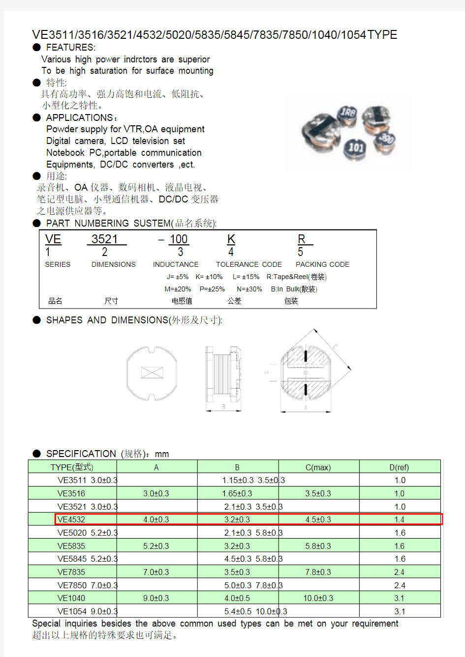
● SHAPES AND DIMENSIONS(外形及尺寸):
VE3511-R47N 0.47 0.72 0.32 100KHz
VE3511-R56N 0.56 0.85 0.20 100KHz VE3511-R68N 0.68 0.93 0.19 100KHz
VE3511-R82N 0.82 1.02 0.185 100KHz VE3511-100K 10 1.15 0.18 100KHz
VE3511-120K 12 1.28 0.175 100KHz VE3511-150K 15 1.32 0.172 100KHz
VE3511-180K 18 1.45 0.17 100KHz VE3511-220K 22 1.55 0.162 100KHz
VE3511-250K 25 1.62 0.160 100KHz VE3511-330K 33 1.70 0.150 100KHz
VE3511-470K 47 1.75 0.150 100KHz VE3511-560K 56 1.82 0.145 100KHz
VE3511-680K 68 1.88 0.142 100KHz VE3511-820K 82 1.92 0.140 100KHz
VE3511-101K 100 2.00 0.138 100KHz VE3511-221K 220 2.10 0.136 100KHz
VE3511-331K 330 2.18 0.132 100KHz VE3511-391K 390 2.45 0.130 100KHz
VE3516 TYPE
PART NUMBER.
品名INDUCTANCE
电感值(μH)
DCR(max)
直流电阻(?)
IDC(max)
定格电流(A)
TEST FREQ.
测试频率
VE3516-2R2N
2.2 0.10 1.8 100KHz VE3516-3R3N
3.3 0.15 1.5 100KHz
VE3516-4R7N
4.7 0.12 1.2 100KHz VE3516-5R6N
5.6 0.24 1.15 100KHz
VE3516-6R8N
6.8 0.26 1.1 100KHz VE3516-100K 10 0.38 0.8 100KHz
VE3516-220K 22 0.65 0.6 100KHz
VE3516-330K 33 0.85 0.45 100KHz
VE3516-470K 47 1.20 0.35 100KHz This indicates the value of current when the inductance is 10% lower than its initial value at D.C
VE3521-2R7M 2.7 0.100 1.90 100KHz
VE3521-3R3M 3.3 0.120 1.80 100KHz VE3521-3R9M 3.9 0.130 1.70 100KHz
VE3521-4R7M 4.7 0.150 1.40 100KHz VE3521-5R6M 5.6 0.180 1.30 100KHz
VE3521-6R8M 6.8 0.190 1.20 100KHz VE3521-8R2M 8.2 0.215 1.10 100KHz
VE3521-100K 10 0.23 0.76 100KHz VE3521-120K 12 0.27 0.685 100KHz
VE3521-150K 15 0.31 0.635 100KHz VE3521-180K 18 0.41 0.525 100KHz
VE3521-220K 22 0.47 0.500 100KHz VE3521-270K 27 0.66 0.405 100KHz
VE3521-330K 33 0.76 0.380 100KHz VE3521-390K 39 0.85 0.355 100KHz
VE3521-470K 47 0.97 0.330 100KHz VE3521-560K 56 1.25 0.290 100KHz
VE3521-680K 68 1.45 0.275 100KHz VE3521-820K 82 1.85 0.235 100KHz
VE3521-101K 100 2.20 0.220 100KHz VE3521-121K 120 2.90 0.185 100KHz
VE3521-151K 150 3.40 0.170 100KHz VE3521-181K 180 3.90 0.165 100KHz
VE3521-221K 220 4.50 0.155 100KHz VE3521-271K 270 6.00 0.135 100KHz
VE3521-331K 330 7.00 0.125 100KHz VE3521-391K 390 7.80 0.115 100KHz
This indicates the value of current when the inductance is 10% lower than its initial value at D.C Superposition or D.C.current when at ⊿t=40℃ whichever is lower.
直流重叠特性,规格内之IDC通过时电感值变化在初始值的-10%以内,温升40℃以内
VE4532-1R4M 1.4 0.038 3.30 100KHz VE4532-1R8M 1.8 0.042 2.91 100KHz VE4532-2R2M 2.2 0.047 2.60 100KHz VE4532-2R7M 2.7 0.052 2.43 100KHz VE4532-3R3M 3.3 0.058 2.15 100KHz VE4532-3R9M 3.9 0.076 1.98 100KHz VE4532-4R7M 4.7 0.094 1.70 100KHz VE4532-5R6M 5.6 0.101 1.60 100KHz VE4532-6R8M 6.8 0.117 1.41 100KHz VE4532-8R2M 8.2 0.132 1.26 100KHz VE4532-100K 10 0.182 1.15 100KHz VE4532-120K 12 0.210 1.05 100KHz VE4532-150K 15 0.235 0.92 100KHz VE4532-180K 18 0.338 0.84 100KHz VE4532-220K 22 0.378 0.76 100KHz VE4532-270K 27 0.522 0.71 100KHz VE4532-330K 33 0.540 0.64 100KHz VE4532-390K 39 0.587 0.59 100KHz VE4532-470K 47 0.844 0.54 100KHz VE4532-560K 56 0.937 0.50 100KHz VE4532-680K 68 1.117 0.48 100KHz VE4532-820K 82 1.20 0.46 100KHz VE4532-121K 120 1.04 0.30 100KHz VE4532-152K 1500 15.0 0.05 100KHz VE4532-172K 1700 16.0 0.04 100KHz This indicates the value of current when the inductance is 10% lower than its initial value at D.C Superposition or D.C.current when at ⊿t=40℃ whichever is lower.
直流重叠特性,规格内之IDC通过时电感值变化在初始值的-10%以内,温升40℃以内
VE5020-2R2M 2.2 0.039 2.16 100KHz VE5020-2R7M 2.7 0.044 2.08 100KHz VE5020-3R3M 3.3 0.049 1.90 100KHz VE5020-3R9M 3.9 0.056 1.84 100KHz VE5020-4R7M 4.7 0.062 1.60 100KHz VE5020-5R6M 5.6 0.078 1.44 100KHz VE5020-6R8M 6.8 0.091 1.36 100KHz VE5020-8R2M 8.2 0.103 1.12 100KHz VE5020-100K 10 0.133 1.04 100KHz VE5020-120K 12 0.148 0.96 100KHz VE5020-150K 15 0.166 0.88 100KHz VE5020-180K 18 0.213 0.77 100KHz VE5020-220K 22 0.248 0.73 100KHz VE5020-270K 27 0.328 0.64 100KHz VE5020-330K 33 0.378 0.58 100KHz VE5020-390K 39 0.438 0.54 100KHz VE5020-470K 47 0.546 0.49 100KHz VE5020-560K 56 0.621 0.45 100KHz VE5020-680K 68 0.715 0.41 100KHz VE5020-820K 82 1.00 0.35 100KHz VE5020-101K 100 1.07 0.35 100KHz VE5020-121K 120 1.25 0.32 100KHz VE5020-151K 150 1.66 0.26 100KHz VE5020-181K 180 1.90 0.23 100KHz VE5020-221K 220 2.44 0.21 100KHz VE5020-271K 270 2.73 0.19 100KHz This indicates the value of current when the inductance is 10% lower than its initial value at D.C Superposition or D.C.current when at ⊿t=40℃ whichever is lower.
直流重叠特性,规格内之IDC通过时电感值变化在初始值的-10%以内,温升40℃以内
VE5835-1R0M 1.0 0.03 4.50 100KHz VE5835-1R2M 1.2 0.03 4.20 100KHz VE5835-1R5M 1.5 0.03 4.10 100KHz VE5835-1R8M 1.8 0.03 3.70 100KHz VE5835-2R2M 2.2 0.03 3.50 100KHz VE5835-2R7M 2.7 0.04 3.20 100KHz VE5835-3R3M 3.3 0.05 2.80 100KHz VE5835-3R9M 3.9 0.06 2.60 100KHz VE5835-4R7M 4.7 0.07 2.50 100KHz VE5835-5R6M 5.6 0.08 2.40 100KHz VE5835-6R8M 6.8 0.09 2.20 100KHz VE5835-8R2M 8.2 0.10 2.00 100KHz VE5835-100K 10 0.12 1.80 100KHz VE5835-120K 12 0.13 1.75 100KHz VE5835-150K 15 0.15 1.70 100KHz VE5835-180K 18 0.18 1.60 100KHz VE5835-220K 22 0.22 1.50 100KHz VE5835-270K 27 0.24 1.40 100KHz VE5835-330K 33 0.30 1.10 100KHz VE5835-390K 39 0.40 1.00 100KHz VE5835-470K 47 0.43 0.90 100KHz VE5835-560K 56 0.50 0.85 100KHz VE5835-680K 68 0.60 0.80 100KHz VE5835-820K 82 0.80 0.65 100KHz VE5835-101K 100 0.90 0.60 100KHz VE5835-121K 120 1.00 0.58 100KHz VE5835-151K 150 1.30 0.43 100KHz VE5835-181K 180 1.50 0.41 100KHz VE5835-221K 220 2.00 0.38 100KHz VE5835-271K 270 2.50 0.35 100KHz VE5835-331K 330 3.20 0.28 100KHz VE5835-391K 390 3.50 0.26 100KHz VE5835-471K 470 4.20 0.20 100KHz VE5835-561K 560 4.50 0.19 100KHz VE5835-681K 680 6.00 0.18 100KHz VE5835-821K 820 6.50 0.15 100KHz VE5835-102K 1000 8.00 0.13 100KHz This indicates the value of current when the inductance is 10% lower than its initial value at D.C Superposition or D.C.current when at ⊿t=40℃ whichever is lower.
VE5845-1R0M 1.0 0.015 5.90 100KHz VE5845-1R2M 1.2 0.020 5.20 100KHz
VE5845-1R5M 1.5 0.025 4.70 100KHz
VE5845-1R8M 1.8 0.030 4.00 100KHz
VE5845-2R2M 2.2 0.035 3.80 100KHz
VE5845-2R7M 2.7 0.040 3.40 100KHz
VE5845-3R3M 3.3 0.045 3.30 100KHz
VE5845-3R9M 3.9 0.050 2.90 100KHz
VE5845-4R7M 4.7 0.060 2.80 100KHz
VE5845-5R6M 5.6 0.070 2.40 100KHz
VE5845-6R8M 6.8 0.080 2.10 100KHz
VE5845-8R2M 8.2 0.090 2.00 100KHz
VE5845-100M 10 0.10 1.44 100KHz
VE5845-120M 12 0.12 1.40 100KHz
VE5845-150M 15 0.14 1.30 100KHz
VE5845-180M 18 0.15 1.23 100KHz
VE5845-220M 22 0.18 1.11 100KHz
VE5845-270M 27 0.20 0.97 100KHz
VE5845-330L 33 0.23 0.88 100KHz
VE5845-390L 39 0.32 0.80 100KHz
VE5845-470L 47 0.37 0.72 100KHz
VE5845-560K 56 0.42 0.68 100KHz
VE5845-680K 68 0.46 0.61 100KHz
VE5845-820K 82 0.60 0.58 100KHz
VE5845-101K 100 0.70 0.52 100KHz
VE5845-121K 120 0.93 0.48 100KHz
VE5845-151K 150 1.10 0.40 100KHz
VE5845-181K 180 1.38 0.38 100KHz
VE5845-221K 220 1.57 0.35 100KHz
VE5845-271K 270 1.65 0.32 100KHz
VE5845-331K 330 1.70 0.28 100KHz
VE5845-391K 390 1.80 0.26 100KHz
VE5845-471K 470 2.30 0.23 100KHz
VE5845-561K 560 2.50 0.20 100KHz
VE5845-681K 680 3.00 0.19 100KHz
VE5845-821K 820 4.50 0.16 100KHz
VE5845-102K 1000 4.80 0.14 100KHz
This indicates the value of current when the inductance is 10% lower than its initial value at D.C Superposition or D.C.current when at ⊿t=40℃ whichever is lower.
VE7835-100K 10 0.080 1.44 100KHz VE7835-120K 12 0.090 1.39 100KHz
VE7835-150K 15 0.100 1.24 100KHz
VE7835-180K 18 0.110 1.12 100KHz
VE7835-220K 22 0.130 1.07 100KHz
VE7835-270K 27 0.150 0.94 100KHz
VE7835-330K 33 0.170 0.85 100KHz VE7835-390K 39 0.220 0.74 100KHz
VE7835-470K 47 0.250 0.68 100KHz
VE7835-560K 56 0.280 0.64 100KHz
VE7835-680K 68 0.330 0.59 100KHz
VE7835-820K 82 0.410 0.54 100KHz
VE7835-101K 100 0.480 0.51 100KHz VE7835-121K 120 0.540 0.49 100KHz
VE7835-151K 150 0.750 0.40 100KHz
VE7835-181K 180 1.020 0.36 100KHz
VE7835-221K 220 1.200 0.31 100KHz
VE7835-271K 270 1.310 0.29 100KHz
VE7835-331K 330 1.500 0.28 100KHz This indicates the value of current when the inductance is 10% lower than its initial value at D.C Superposition or D.C.current when at ⊿t=40℃ whichever is lower.
直流重叠特性,规格内之IDC通过时电感值变化在初始值的-10%以内,温升40℃以内
VE7850-120M 12 0.080 2.00 100KHz VE7850-150M 15 0.090 1.80 100KHz VE7850-180M 18 0.100 1.60 100KHz VE7850-220M 22 0.110 1.50 100KHz VE7850-270M 27 0.120 1.30 100KHz VE7850-330M 33 0.130 1.20 100KHz VE7850-390M 39 0.160 1.10 100KHz VE7850-470M 47 0.180 1.10 100KHz VE7850-560K 56 0.240 0.94 100KHz VE7850-680K 68 0.280 0.85 100KHz VE7850-820K 82 0.370 0.78 100KHz VE7850-101K 100 0.430 0.72 100KHz VE7850-121K 120 0.470 0.66 100KHz VE7850-151K 150 0.640 0.58 100KHz VE7850-181K 180 0.710 0.51 100KHz VE7850-221K 220 0.960 0.49 100KHz VE7850-271K 270 1.110 0.42 100KHz VE7850-331K 330 1.260 0.40 100KHz VE7850-391K 390 1.770 0.36 100KHz VE7850-471K 470 1.960 0.34 100KHz This indicates the value of current when the inductance is 10% lower than its initial value at D.C Superposition or D.C.current when at ⊿t=40℃ whichever is lower.
直流重叠特性,规格内之IDC通过时电感值变化在初始值的-10%以内,温升40℃以内
VE1040-120K 12 0.061 2.13 100KHz VE1040-150K 15 0.070 1.87 100KHz VE1040-180K 18 0.081 1.73 100KHz VE1040-220K 22 0.088 1.60 100KHz VE1040-270K 27 0.100 1.44 100KHz VE1040-330K 33 0.120 1.26 100KHz VE1040-390K 39 0.151 1.20 100KHz VE1040-470K 47 0.170 1.10 100KHz VE1040-560K 56 0.199 1.01 100KHz VE1040-680K 68 0.223 0.91 100KHz VE1040-820K 82 0.252 0.85 100KHz VE1040-101K 100 0.344 0.74 100KHz VE1040-121K 120 0.396 0.69 100KHz VE1040-151K 150 0.544 0.61 100KHz VE1040-181K 180 0.621 0.56 100KHz VE1040-221K 220 0.721 0.53 100KHz VE1040-271K 270 0.949 0.45 100KHz VE1040-331K 330 1.100 0.42 100KHz VE1040-391K 390 1.245 0.38 100KHz VE1040-471K 470 1.526 0.35 100KHz VE1040-561K 560 1.904 0.32 100KHz This indicates the value of current when the inductance is 10% lower than its initial value at D.C Superposition or D.C.current when at ⊿t=40℃ whichever is lower.
直流重叠特性,规格内之IDC通过时电感值变化在初始值的-10%以内,温升40℃以内
VE1054-120M 12 0.070 2.45 100KHz VE1054-150M 15 0.080 2.27 100KHz VE1054-180M 18 0.090 2.15 100KHz VE1054-220M 22 0.100 1.95 100KHz VE1054-270M 27 0.110 1.76 100KHz VE1054-330L 33 0.120 1.50 100KHz VE1054-390L 39 0.140 1.37 100KHz VE1054-470L 47 0.170 1.28 100KHz VE1054-560K 56 0.190 1.17 100KHz VE1054-680K 68 0.220 1.11 100KHz VE1054-820K 82 0.250 1.00 100KHz VE1054-101K 100 0.350 0.97 100KHz VE1054-121K 120 0.400 0.89 100KHz VE1054-151K 150 0.470 0.78 100KHz VE1054-181K 180 0.630 0.72 100KHz VE1054-221K 220 0.730 0.66 100KHz VE1054-271K 270 0.970 0.57 100KHz VE1054-331K 330 1.150 0.52 100KHz VE1054-391K 390 1.300 0.48 100KHz VE1054-471K 470 1.480 0.42 100KHz VE1054-561K 560 1.900 0.33 100KHz VE1054-681K 680 2.250 0.28 100KHz VE1054-821K 820 2.550 0.24 100KHz This indicates the value of current when the inductance is 10% lower than its initial value at D.C Superposition or D.C.current when at ⊿t=40℃ whichever is lower.
直流重叠特性,规格内之IDC通过时电感值变化在初始值的-10%以内,温升40℃以内
卷轴尺寸 (REEL DIMENSIONS) 如下图:
卷轮尺寸(REEL DIMENSIONS)一般公差±0.5mm
型号unit ФA ФB ФC W D
mm 330 100 13.5 12.5 18.5 Φ13”REEL-12G
inch 13.0 3.94 0.482 0.492 0.728
mm 330 100 13.5 16.5 22.5 Φ13”REEL-16G
inch 13.0 3.94 0.482 0.650 0.889
mm 330 100 13.5 24.5 30.5 Φ13”REEL-24G
inch 13.0 3.94 0.482 0.965 1.201
◆ 包装(Packing)
品名规格卷轮型号每卷包装数量
(PCS)
每啤盒包装数量(PCS)
(尺寸:338x338x78mm)
每箱包装数量(PCS)
(尺寸:350x350x170mm)
VE3511 Φ13”REEL-12G 3000 12000 24000 VE3516 Φ13”REEL-12G 3000 12000 24000 VE3521 Φ13”REEL-12G 3000 12000 24000 VE4532 Φ13”REEL-12G 2000 8000 16000 VE5020 Φ13”REEL-12G 3000 12000 24000 VE5835 Φ13”REEL-12G 1500 6000 12000 VE5845 Φ13”REEL-12G 1500 6000 12000 VE7835 Φ13”REEL-16G 1000 3000 6000
VE7850 Φ13”REEL-16G 1000 3000 6000 VE1040 Φ13”REEL-24G 1000 2000 4000
VE1054 Φ13”REEL-24G 1000 2000 4000 Special inquiries besides the above common used types can be met on your requirement
超出以上规格的特殊要求也可满足。
VE 3511/3516/3521/4532/5020/5835/5845/7835/7850/1040/1054TYPE ● FEATURES: Various high power indrctors are superior To be high saturation for surface mounting ● 特性: 具有高功率、强力高饱和电流、低阻抗、 小型化之特性。 ● APPLICATIONS : Powder supply for VTR,OA equipment Digital camera, LCD television set Notebook PC,portable communication Equipments, DC/DC converters ,ect. ● 用途: 录音机、OA 仪器、数码相机、液晶电视、 笔记型电脑、小型通信机器、DC/DC 变压器 之电源供应器等。 ● PART NUMBERING SUSTEM(品名系统): ● SHAPES AND DIMENSIONS(外形及尺寸):
VE3511-R47N 0.47 0.72 0.32 100KHz VE3511-R56N 0.56 0.85 0.20 100KHz VE3511-R68N 0.68 0.93 0.19 100KHz VE3511-R82N 0.82 1.02 0.185 100KHz VE3511-100K 10 1.15 0.18 100KHz VE3511-120K 12 1.28 0.175 100KHz VE3511-150K 15 1.32 0.172 100KHz VE3511-180K 18 1.45 0.17 100KHz VE3511-220K 22 1.55 0.162 100KHz VE3511-250K 25 1.62 0.160 100KHz VE3511-330K 33 1.70 0.150 100KHz VE3511-470K 47 1.75 0.150 100KHz VE3511-560K 56 1.82 0.145 100KHz VE3511-680K 68 1.88 0.142 100KHz VE3511-820K 82 1.92 0.140 100KHz VE3511-101K 100 2.00 0.138 100KHz VE3511-221K 220 2.10 0.136 100KHz VE3511-331K 330 2.18 0.132 100KHz VE3511-391K 390 2.45 0.130 100KHz VE3516 TYPE PART NUMBER. 品名INDUCTANCE 电感值(μH) DCR(max) 直流电阻(?) IDC(max) 定格电流(A) TEST FREQ. 测试频率 VE3516-2R2N 2.2 0.10 1.8 100KHz VE3516-3R3N 3.3 0.15 1.5 100KHz VE3516-4R7N 4.7 0.12 1.2 100KHz VE3516-5R6N 5.6 0.24 1.15 100KHz VE3516-6R8N 6.8 0.26 1.1 100KHz VE3516-100K 10 0.38 0.8 100KHz VE3516-220K 22 0.65 0.6 100KHz VE3516-330K 33 0.85 0.45 100KHz VE3516-470K 47 1.20 0.35 100KHz This indicates the value of current when the inductance is 10% lower than its initial value at D.C
Wire Wound SMD Power Inductors – SWPA Series Operating temperature range: -40℃~+125℃ (Including self-heating) FEATURES ● Magnetic-resin shielded construction reduces buzz noise to ultra-low levels ● Metallization on ferrite core results in excellent shock resistance and damage-free durability ● Closed magnetic circuit design reduces leakage flux and Electro Magnetic Interference (EMI) ● 30% higher current rating than conventional inductors of equal size ● Takes up less PCB real estate and save more power APPLICATIONS ● Smart phone, smart TV, set top box, notebook ● Car navigation systems, telecomm base stations ● VR, AR ● LED lighting PRODUCT IDENTIFICATION SWPA 3012 S 1R0 N T □□□ ① ② ③ ④ ⑤ ⑥ ⑦ ② External Dimensions (L×W×H) [mm] 252010 2.5×2.0×1.0 252012 2.5×2.0×1.2 3010 3.0×3.0×1.0 3012 3.0×3.0×1.2 3015 3.0×3.0×1.5 4010 4.0×4.0×1.0 4012 4.0×4.0×1.2 4018 4.0×4.0×1.8 4020 4.0×4.0×2.0 4026 4.0×4.0×2.6 4030 4.0×4.0×3.0 5012 5.0×5.0×1.2 5020 5.0×5.0×2.0 5040 5.0×5.0×4.0 6020 6.0×6.0×2.0 6028 6.0×6.0×2.8 6040 6.0×6.0×4.0 6045 6.0×6.0×4.5 8040 8.0×8.0×4.0 8050 8.0×8.0×5.0 8060 8.0×8.0×6.0 8065 8.0×8.0×6.5 ① Type SWPA Wire Wound SMD Power Inductor ③ Feature Type S Standard ④ Nominal Inductance Example Nominal Value 1R0 1.0μH 100 10μH ⑤ Inductance Tolerance K ±10% M ±20% N ±30% ⑥ Packing T Tape Carrier Package ⑦ Design Code □□□ Standard product is blank https://www.doczj.com/doc/034338842.html,
MURS120T3G Series, SURS8120T3G Series, NRVUS120VT3G Series Surface Mount Ultrafast Power Rectifiers MURS105T3G, MURS110T3G, MURS115T3G, MURS120T3G, MURS140T3G, MURS160T3G, SURS8105T3G, SURS8110T3G, SURS8115T3G, SURS8120T3G, SURS8140T3G, SURS8160T3G, NRVUS110VT3G, NRVUS120VT3G, NRVUS160VT3G Ideally suited for high voltage, high frequency rectification, or as free wheeling and protection diodes in surface mount applications where compact size and weight are critical to the system. Features ?Small Compact Surface Mountable Package with J?Bend Leads ?Rectangular Package for Automated Handling ?High Temperature Glass Passivated Junction ?Low Forward V oltage Drop (0.71 to 1.05 V Max @ 1.0 A, T J = 150°C)?NRVUS and SURS8 Prefixes for Automotive and Other Applications Requiring Unique Site and Control Change Requirements; AEC?Q101 Qualified and PPAP Capable ?These Devices are Pb?Free, Halogen Free/BFR Free and are RoHS Compliant Mechanical Characteristics: ?Case: Epoxy, Molded ?Weight: 95 mg (Approximately) ?Finish: All External Surfaces Corrosion Resistant and Terminal Leads are Readily Solderable ?Lead and Mounting Surface Temperature for Soldering Purposes: 260°C Max. for 10 Seconds ?Polarity: Polarity Band Indicates Cathode Lead ?ESD Rating: ?Human Body Model = 3B (> 8 kV) ?Machine Model = C (> 400 V)See detailed ordering and shipping information in the table on page 2 of this data sheet. ORDERING INFORMATION MARKING DIAGRAM See general marking information in the device marking table on page 2 of this data sheet. DEVICE MARKING INFORMATION ULTRAFAST RECTIFIERS 1.0 AMPERE, 50?600 VOLTS SMB CASE 403A https://www.doczj.com/doc/034338842.html, A=Assembly Location* Y=Year WW=Work Week U1=Device Code x = A, B, C, D, G, or J G=Pb?Free Package AYWW U1x G G (Note: Microdot may be in either location) * The Assembly Location code (A) is front side optional. In cases where the Assembly Location is stamped in the package bottom (molding ejecter pin), the front side assembly code may be blank.
E12 SERIES SPECIFICATION 1/5
E12 SERIES SPECIFICATION 2/5
E12 SERIES SPECIFICATION
项目ITEM 7-1.Rotational life 回转寿命 在无负荷条件下轴以600~1000周/小时速度回转30000周。7-2.Damp heat 耐湿性 7-3、Dry heat 耐热性 7-4. Cold 低温特性 7-5. Solder ability 焊锡性 7-6.Resistance to Soldering heat 耐焊接热 Soldering:Solder temperature:260±5℃ or less Immersion time:within 3S 焊接:温度260±5℃或以下,时间3秒以内. 2.Preheating time:within 1 min.接触无异常. 预热:基板表面温度100℃以下,时间1分钟以内.使用基板:t=1.6mm的单面覆铜板. mechanical abnormality.Preheating:1.Surface temperature of board:100℃ or less.不得有绝缘体的破损、变形、Printed wiring board:single-sided copper clad laminate Electrical characteristics board with thickness of 1.6mm.shall be satisfied No 温度300℃以下,时间3秒以内.Dip soldering.槽焊 Manual soldering 手工焊接 Bit temperature of soldering iron:300℃ less than Application time of soldering iron:within 3s 端子在260℃±5℃温度的焊锡槽内浸锡3秒±0.5秒.surface being immersed. 浸渍面须有75%以上焊锡附着 The terminals shall be immersed into solder bath at 260℃ A new uniform coating of solder for 3s±0.5s in the same manner as para.shall cover 75% minimum of the 温度-25±3℃的恒温箱中放置96±4小时,常温、常湿放置1.5小时后测试. shall be subjected to standard atmospheric conditions for 所有项应满足初期规格 1.5H.After which measurements shall be made. The encoder shall be stored at a temperature of -25±3℃ Specifications in clause all for 96±4H in a thermostatic chamber.And then the encoder items is shall be satisfied.温度80±3℃的恒温箱中放置96±4小时,常温、常湿放置1.5小时后测试. shall be subjected to standard atmospheric conditions for 所有项应满足初期规格 1.5H,After which measurements shall be made. E12 SERIES SPECIFICATION E E121212系列规格书 系列规格书 4/5 7 7 耐久性能 耐久性能 耐久性能 ENDURANCE CHARACTERISTICS ENDURANCE CHARACTERISTICS 条件规格CONDITIONS SPECIFICATIONS The shaft of encoder shall be rotated to 30000 cycles at a ≤5mS Bounce t2≤3mS 突跳 t2≤Chattiring t1,t3≤5mS 振荡t1,t3speed of 600~1000 cycles/H without electrical load,after 3mSDetent feeling has to with measurements shall be made. remains 尚余有轻微定位感Specifications in clause all relative humidity of 90% to95% for96±4H in a thermostatic items is shall be satisfied.Contact resistance 200Ω Max 端子间接触阻抗200Ω以下The encoder shall be stored at temperature of 40±2℃ with shall be made.温度40±2℃,湿度90~95%的恒温恒湿槽中放置96±4小时后,在常温、常湿中放置1.5小时后测试. The encoder shall be stored at a temperature of 80±3℃ Specifications in clause all for 96±4H in a thermostatic chamber.And then the encoder items is shall be satisfied.chamber.And the encoder shall be subjected to standard at- 所有项应满足初期规格 mospheric conditions for 1.5H,After which measurements
LM393, LM393E, LM293, LM2903, LM2903E, LM2903V, NCV2903 Low Offset Voltage Dual Comparators The LM393 series are dual independent precision voltage comparators capable of single or split supply operation. These devices are designed to permit a common mode range?to?ground level with single supply operation. Input offset voltage specifications as low as 2.0 mV make this device an excellent selection for many applications in consumer, automotive, and industrial electronics. Features ?Wide Single?Supply Range: 2.0 Vdc to 36 Vdc ?Split?Supply Range: ±1.0 Vdc to ±18 Vdc ?Very Low Current Drain Independent of Supply V oltage: 0.4 mA ?Low Input Bias Current: 25 nA ?Low Input Offset Current: 5.0 nA ?Low Input Offset V oltage: 5.0 mV (max) LM293/393 ?Input Common Mode Range to Ground Level ?Differential Input V oltage Range Equal to Power Supply V oltage ?Output V oltage Compatible with DTL, ECL, TTL, MOS, and CMOS Logic Levels ?ESD Clamps on the Inputs Increase the Ruggedness of the Device without Affecting Performance ?NCV Prefix for Automotive and Other Applications Requiring Unique Site and Control Change Requirements; AEC?Q100 Qualified and PPAP Capable ?These Devices are Pb?Free, Halogen Free/BFR Free and are RoHS Compliant Figure 1. Representative Schematic Diagram (Diagram shown is for 1 comparator)See detailed marking information and ordering and shipping information on pages 6 and 7 of this data sheet. DEVICE MARKING AND ORDERING INFORMATION PDIP?8 N SUFFIX CASE 626 8 SOIC?8 D SUFFIX CASE 751 1 PIN CONNECTIONS (Top View) Inputs A Inputs B Output B CC https://www.doczj.com/doc/034338842.html, Micro8E DM SUFFIX CASE 846A 1
FEATURES APPLICATIONS 150 M T HOW TO ORDER DIMENSIONS PS-D PS-D SERIES SMD POWER INDUCTORS , Low profile Magnetic shielded SMT type,suitable for reflow soldering. Portable communication equipment Notebook Computer DC/DC DC/DC converters etc. PS 5D28 (Unit)mm
ELECTRICAL CHARACTERISTICS Isat:Isat 35% Isat:Saturation Current,the current when the inductance becomes 35%lower than its initial value. Unit mm PS2D11Series PS2D14Series PS-D SERIES SHIELDED SMD POWER INDUCTORS PS-D PS2D18Series
PS3D18Series PS4D18Series PS4D28Series Isat:Isat35% Isat:Saturation Current,the current when the inductance becomes35%lower than its initial value.
Isat:Isat 35% Isat:Saturation Current,the current when the inductance becomes 35%lower than its initial value. PS5D28Series PS6D28Series PS-D SERIES SHIELDED SMD POWER INDUCTORS PS-D PS6D38Series
有关本公司产品的注意事项 请务必在使用本公司产品目录之前阅读。 注意事项 ■本软件中记载的内容是2011年10月现在的内容。本产品目录记载的内容由于产品的改良等原因发生变更时,恕不另行通知。在您定购我司产品之前请确认最新的产品信息。 当您计划在本软件记载内容,或是《交货规格书》的规定范围以外使用我司产品时,由于使用我司产品引起的该应用设备的瑕疵我司将不承担任何责任。 ■有关详细的产品规格我们准备有《交货规格书》,请向我司咨询相关事宜。 ■在您使用我司产品时,请务必进行应用设备实装状态以及应用产品实际使用环境下的测评。 ■本软件中记载的电子元器件,电路产品等产品适用于一般电子设备。『AV设备,OA设备,家电及办公设备,信息/通讯设备(手机,电脑等)』当您计划把本产品目录中记载的产品使用于可能会危及第三方生命安全的应用设备时,请务必提前与我公司取得联系,针对产品信息加以确认。【运输用设备(火车控制设备,船舶控制设备等),交通用信号设备,防灾设备,医疗用设备,公共性高的信息通信设备等(电话程控交换机,电话,无线电,电视信号等基地局)】 另外,请不要在要求高度安全性,可靠性的应用设备上使用本产品目录中记载的产品。【航天设备,航空设备,核控制设备,用于海底的设备,军事设备等】 同时,应用于安全性,可靠性要求较高的一般电子设备/电路时,请充分进行安全性测评,必要时请在设计过程中追加保护电路。 ■本软件中所记载的内容适用于通过我司营业所,销售子公司,销售代理店(即正规销售渠道)购买的我司产品。通过其他渠道购买的我司产品不在适用范围之内。 ■由于使用本软件记载的产品引起的有关第三方知识产权的冲突,我司概不负责。本产品目录不代表相关权利的实施许诺。 ■有关出口的注意事项 本软件中记载的产品中,部分产品在出口时会被归为“外汇及外贸管理法,美国出口管理法规”的管制货物,请及时实施相关手续,依据相关法律法规进行出口。需确认时,可向我司咨询。
DFE201610E Inductance Range: 0.24~10μH (Unit: mm) (Unit: mm) ? Miniature size: 2016 footprint (2.0mm×1.6mm) and low profile(1.0mm Max. height) ? The use of magnetic iron powder ensure capability for large current. ? The use of Flat wire for Low DC resistance. ? Magnetically shielded, low audible core noise. ? Reflow solderable. ? Operating temperature : -40~+125°C ? 小型薄型構造 (2.0x1.6mm角、高さ1.0mm Max.) ? 磁性材に鉄系磁性粉を用いた大電流対応 ? 平角線採用による低直流抵抗 ? 閉磁路構造、低コア鳴きノイズ ? リフロはんだ対応 ? 動作温度範囲:-40~+125°C (1) Inductance is measured with a LCR meter 4284A (Agilent Technologies ) or equivalent. Test frequency at 1MHz (2) DC resistance is measured with 34420A (Agilent Technologies) or 3541(HIOKI). (Reference ambient temperature 20°C) (3) Inductance Decrease Current based upon 30% inductance reduction from the initial value (4) Temperature Rise Current based upon 40°C temperature rise. (Reference ambient temperature 20°C) (1) インダクタンスはLCR メータ4284A (Agilent Technologies ) または同等品により測定する。測定周波数は1MHz 。 (2) 直流抵抗は測定器34420A (Agilent Technologies )または3541(HIOKI )と同等品により測定する。(周囲温度20°C ) (3) 直流重畳許容電流:直流重畳電流を流した時インダクタンスの値が初期値より30%減少する直流電流値 (4) 温度上昇許容電流:コイルの温度が40°C 上昇する値 (周囲温度20°C を基準とする。) Recommended patterns 推奨パターン図 Metal Alloy Inductors メタルアロイ? インダクタ
DSK32 THRU DSK310SURFACE MOUNT SCHOTTKY BARRIER RECTIFIER Reverse Voltage - 20 to 100 Volts Forward Current -3.0 Ampere 1of 2
RATINGS AND CHARACTERISTIC CURVES DSK32 THRU DSK310 FIG. 3-TYPICAL INSTANTANEOUS FORWARD CHARACTERISTICS NUMBER OF CYCLES AT 60 Hz FIG. 2-MAXIMUM NON-REPETITIVE PEAK FORWARD FIG. 1- FORWARD CURRENT DERATING CURVE A V E R A G E F O R W A R D R E C T I F I E D C U R R E N T ,A M P E R E S I N S T A N T A N E O U S F O R W A R D C U R R E N T ,A M P E R E S P E A K F O R W A R D S U R G E C U R R E N T ,A M P E R E S INSTANTANEOUS FORWARD VOLTAGE, VOLTS 100 10 1 0.1 0.010.001 PERCENT OF PEAK REVERSE VOLTAGE,% FIG. 4-TYPICAL REVERSE CHARACTERISTICS I N S T A N T A N E O U S R E V E R S E C U R R E N T ,M I L L I A M P E R E S AMBIENT TEMPERATURE, C 2of 2
1.一般事项 General requirements 1.1 适用范围Scope of Application 本插座适用于打印机、彩色液晶电视接收机、电脑以及网络等电子设备 外接数字信号装置之用。 This socket is used by color TV, component stereo, video disc players, computers and equivalent electronic equipment to connect with external audio and video device. 1.2 标准状态Standard State 除另规定外,测量应在以下状态进行: The test should be tested in the following state unless otherwise specified 温度: 15℃~ 35℃ Temperature: 15℃~ 35℃ 相对湿度: 45% ~ 70% Relative Humidity: 45% ~ 70% 气压: 86K pa ~ 106 K pa Air Pressure: 86K pa ~ 106 K pa 1.3 使用温度范围:-25℃~ +70℃ Operating Temperature Range:-25℃~ +70℃ 1.4 环保要求:符合欧盟RoHS 指令的环保要求。 Environmental Requirement:Comply with the EU environmental requirements ofRoHS directive 2. 额定规格 Rated voltage and current a.额定电压为:(AC、DC、34 V) Rated voltage: AC, DC, 34V b.额定电流为:2.0 A Rated current: 2.0 A 3. 测试要求 Test Requirements 3.1 外观、机械性能 Appearance & Mechanical Performance:
KBP3005K THRU KBP310K SILICON BRIDGE RECTIFIERS Reverse Voltage - 50 to 1000 Volts Forward Current -3.0 Amperes
RATINGS AND CHARACTERISTIC CURVES KBP3005K THRU KBP310K 1.0 2.0 3.0 50 100 150 I ,A V E R A G E R E C T I F I E D C U R R E N T (A ) O T,TEMPERATURE (°C) 10 100 C , J U N C T I O N C A P A C I T A N C E (p F ) j V , REVERSE VOLTAGE (V) Fig. 4Typical Junction Capacitance R 00.1 1.0 10 0.2 0.4 0.6 0.8 1.0 1.2 1.4 I ,I N S T A N T A N E O U S F W D C U R R E N T (A ) F V ,INSTANTANEOUS FWD VOL TAGE (V) Fig.2T ypical Fwd Characteristics F Fig. 1 Forward Current Derating Curve Fig.3Max Non-Repetitive P eak Fwd Surge Current 50 40 100 30 I F S M ,P E A K F W D S U R G E C U R R E N T (A ) 10 NUMBER OF CYCLES AT 60 Hz 60 100
DCR SRF I sat (A)4 I rms (A)5Inductance 2max typ 310%20%30%20°C 40°C Part number 1(μH)(Ohms)(MHz)drop drop drop rise rise MSS7341-332NL_ 3.3 ±30%0.02058.0 2.74 3.28 3.72 3.95 5.00MSS7341-502NL_ 5.0 ±30%0.02446.0 2.30 2.82 3.16 3.40 4.70MSS7341-622NL_ 6.2 ±30%0.02742.0 2.18 2.66 2.98 3.05 4.30MSS7341-742NL_7.4 ±30%0.03140.0 1.92 2.32 2.56 2.80 4.10MSS7341-872NL_8.7 ±30%0.03435.0 1.78 2.12 2.36 2.80 3.90MSS7341-103ML_10 ±20%0.03832.0 1.64 1.92 2.10 2.80 3.80MSS7341-123ML_12 ±20%0.05326.2 1.48 1.76 1.92 2.45 3.30MSS7341-153ML_15 ±20%0.05724.0 1.36 1.60 1.78 2.05 3.00MSS7341-183ML_18 ±20%0.07822.5 1.20 1.46 1.62 1.85 2.65MSS7341-223ML_22 ±20%0.08221.5 1.02 1.26 1.42 1.70 2.35MSS7341-273ML_27 ±20%0.10919.0 1.00 1.14 1.22 1.50 2.10MSS7341-333ML_33 ±20%0.12418.00.91 1.04 1.16 1.50 1.95MSS7341-393ML_39 ±20%0.13817.00.85 1.01 1.12 1.50 1.90MSS7341-473ML_47 ±20%0.15514.20.740.92 1.00 1.50 1.85MSS7341-563ML_56 ±20%0.20213.40.680.800.87 1.25 1.60MSS7341-683ML_68 ±20%0.27612.00.620.730.80 1.00 1.35MSS7341-823ML_82 ±20%0.32411.00.570.660.72 1.00 1.25MSS7341-104ML_100 ±20%0.35810.50.540.640.710.90 1.15MSS7341-224ML_220 ±20%0.780 5.00.350.410.470.570.78MSS7341-474ML_ 470 ±20% 1.45 3.0 0.240.280.320.430.57 Designer’s Kit C385 contains 3 each of all values.Core material Ferrite Core and winding loss See https://www.doczj.com/doc/034338842.html,/coreloss Terminations RoHS compliant matte tin over nickel over phos bronze (current production) or gold over nickel over phos bronze (prior production). Other terminations available at additional cost.Weight:0.61 – 0.67 g Ambient temperature –40°C to +85°C with I rms current, +85°C to +125°C with derated current Storage temperature Component: –40°C to +125°C.Packaging: –40°C to +80°C Resistance to soldering heat Max three 40 second reflows at +260°C, parts cooled to room temperature between cycles Moisture Sensitivity Level (MSL)1 (unlimited floor life at <30°C /85% relative humidity) Failures in Time (FIT) / Mean Time Between Failures (MTBF)38 per billion hours / 26,315,789 hours, calculated per Telcordia SR-332Packaging 1200/13″ reel;Plastic tape:16 mm wide, 0.35 mm thick, 12 mm pocket spacing, 4.5 mm pocket depth PCB washing Only pure water or alcohol recommended ?6.6 × 6.6 mm footprint; 4.1 mm high shielded inductors ?Low DCR and excellent current handling 1.Please specify termination and packaging codes:MSS7341-474M LD Termination:L =RoHS compliant matte tin over nickel over phos bronze (current production) or gold over nickel over phos bronze (prior production)Special order: T = RoHS tin-silver-copper (95.5/4/0.5)over gold over nickel over phos bronze or S = non-RoHS tin-lead (63/37) over gold over nickel over phos bronze. Packaging:D =13″ machine-ready reel. EIA-481 embossed plastic tape (1200 parts per full reel). B =Less than full reel. In tape, but not machine ready. To have a leader and trailer added ($25 charge), use code letter D instead. 2.Inductance measured at 100 kHz, 0.1 Vrms, 0 Adc using a Coilcraft SMD-A fixture in an Agilent/HP 4263B LCR meter. 3.SRF measured using an Agilent/HP 8753D network analyzer and a Coilcraft SMD-D test fixture. 4.DC current at which the inductance drops the specified amount from its value without current. 5.Current that causes the specified temperature rise from 25°C ambient. 6.Electrical specifications at 25°C. Refer to Doc 362 “Soldering Surface Mount Components”before soldering.
光纤F C系列规格书 Pleasure Group Office【T985AB-B866SYT-B182C-BS682T-STT18】
目录 1.应用范围‥‥‥‥‥‥‥‥‥‥‥‥‥‥‥‥‥‥‥‥‥‥1 系列跳线‥‥‥‥‥‥‥‥‥‥‥‥‥‥‥‥‥‥‥‥1 材质‥‥‥‥‥‥‥‥‥‥‥‥‥‥‥‥‥‥‥‥‥‥‥1 规格、尺寸‥‥‥‥‥‥‥‥‥‥‥‥‥‥‥‥‥‥‥‥1 性能指标‥‥‥‥‥‥‥‥‥‥‥‥‥‥‥‥‥‥‥‥‥9 实验内容‥‥‥‥‥‥‥‥‥‥‥‥‥‥‥‥‥‥‥‥‥10 产品图片‥‥‥‥‥‥‥‥‥‥‥‥‥‥‥‥‥‥‥‥‥12 一体式适配器‥‥‥‥‥‥‥‥‥‥‥‥‥‥‥‥‥‥ 12 材质‥‥‥‥‥‥‥‥‥‥‥‥‥‥‥‥‥‥‥‥‥‥‥12 规格、尺寸‥‥‥‥‥‥‥‥‥‥‥‥‥‥‥‥‥‥‥‥13 性能指标‥‥‥‥‥‥‥‥‥‥‥‥‥‥‥‥‥‥‥‥‥14 1.应用范围 本规格书适用于FC型光纤活动连接器(跳线、适配器)的生产、检验和使用 FC型光纤活动连接器是一种以单芯插头和适配器为基础组成的螺纹旋转式连接器,它的特点是光纤镶嵌在标称直径为的高精密插针圆柱体中,两插头用M8×的螺帽和适配器进行螺纹连接。 使用条件: 工作温度:-25℃——+70℃ 贮运温度:-40℃——+85℃ 相对湿度:不大于95%(+40℃时)
大气压力:70Kpa——106Kpa 系列跳线、尾纤 材质 金属件:弹簧、外螺、内框、止动环、喇叭口、压环、尾座 陶瓷件:插芯 塑料件:尾套、防尘帽 光缆:二氧化硅、芳族聚酸胺、聚氯乙烯 如需符合ROHS,需在评审单上注明。 外观 产品外观应平滑洁净,金属零件表面无毛刺、油污、伤痕、裂纹及锈蚀现象,塑料、橡胶零件表面应平整、光滑、颜色均匀、一致性好、无裂纹现象。默认光纤/光缆外皮颜色:单模紧套光纤(φ)外皮采用白色,多模紧套光纤(φ)外皮采用白色,单模光缆(φ2和φ3)外皮采用黄色,多模光缆(φ2和φ3)外皮采用橙色,光纤/光缆表面应圆整光滑,光缆上所印字迹应清晰,不允许有拖墨、漏印、错印、重叠、少墨等不良现象。 规格、尺寸 连接头规格、尺寸 FC连接头散件采用细螺纹外框,橡胶尾套,PC为黑色,APC为绿色,使用内置式尾套。如有特殊要求,需在评审单上注明。 FC/PC光纤连接头规格图 FC/PC光纤连接头尺寸