
https://www.doczj.com/doc/3011762318.html,
FEATURES DESCRIPTION
APPLICATIONS
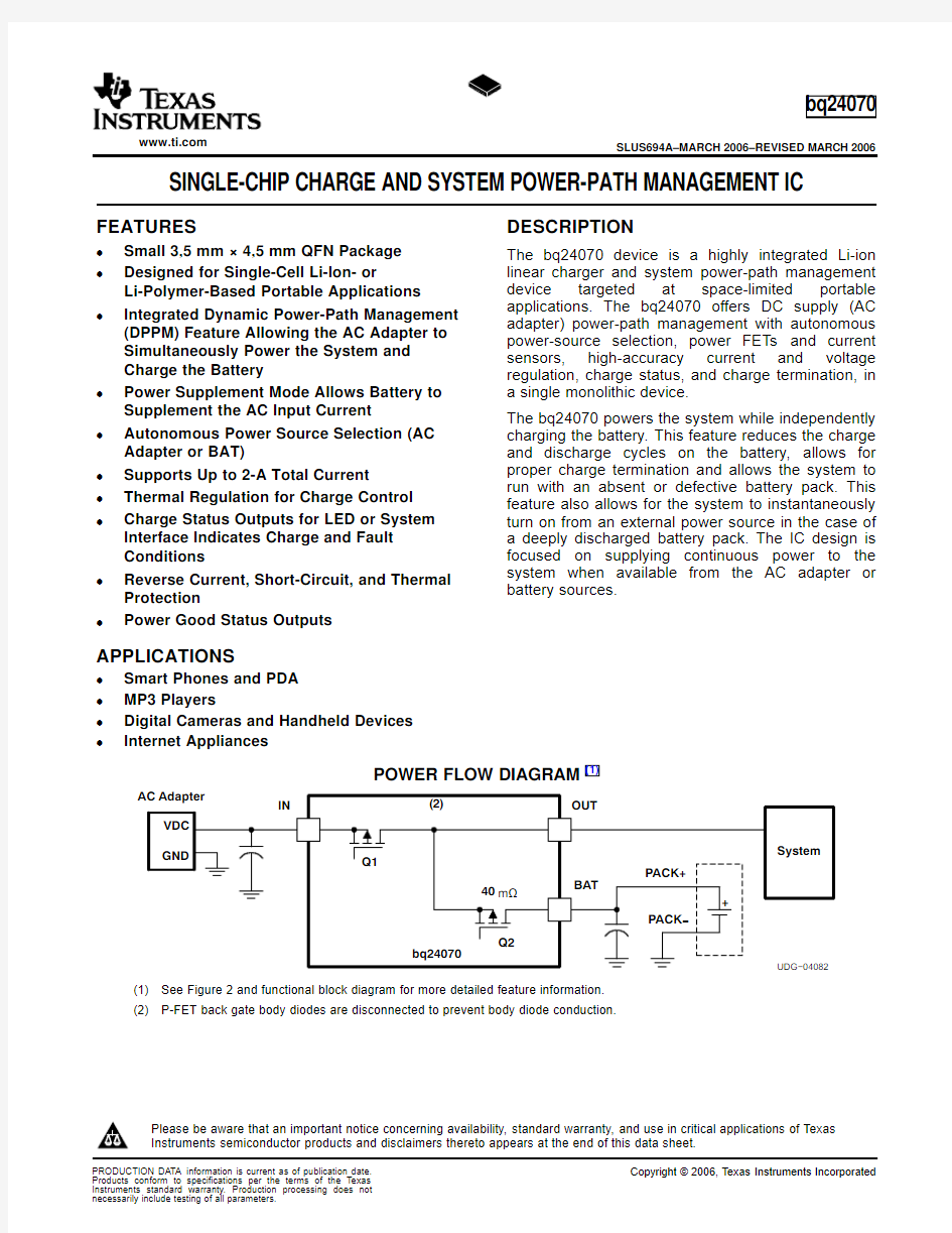
POWER FLOW DIAGRAM
(1)
bq24070
SLUS694A–MARCH2006–REVISED MARCH2006 SINGLE-CHIP CHARGE AND SYSTEM POWER-PATH MANAGEMENT IC
?Small3,5mm×4,5mm QFN Package The bq24070device is a highly integrated Li-ion
linear charger and system power-path management ?Designed for Single-Cell Li-Ion-or
device targeted at space-limited portable Li-Polymer-Based Portable Applications
applications.The bq24070offers DC supply(AC ?Integrated Dynamic Power-Path Management
adapter)power-path management with autonomous (DPPM)Feature Allowing the AC Adapter to power-source selection,power FETs and current Simultaneously Power the System and sensors,high-accuracy current and voltage Charge the Battery regulation,charge status,and charge termination,in
a single monolithic device.
?Power Supplement Mode Allows Battery to
Supplement the AC Input Current The bq24070powers the system while independently ?Autonomous Power Source Selection(AC charging the battery.This feature reduces the charge Adapter or BAT)and discharge cycles on the battery,allows for
proper charge termination and allows the system to ?Supports Up to2-A Total Current
run with an absent or defective battery pack.This ?Thermal Regulation for Charge Control feature also allows for the system to instantaneously
?Charge Status Outputs for LED or System turn on from an external power source in the case of
a deeply discharged battery pack.The IC design is
Interface Indicates Charge and Fault
focused on supplying continuous power to the Conditions
system when available from the AC adapter or ?Reverse Current,Short-Circuit,and Thermal
battery sources.
Protection
?Power Good Status Outputs
?Smart Phones and PDA
?MP3Players
?Digital Cameras and Handheld Devices
?Internet Appliances
(1)See Figure2and functional block diagram for more detailed feature information.
(2)P-FET back gate body diodes are disconnected to prevent body diode conduction.
Please be aware that an important notice concerning availability,standard warranty,and use in critical applications of Texas
Instruments semiconductor products and disclaimers thereto appears at the end of this data sheet.
PRODUCTION DATA information is current as of publication date.Copyright?2006,Texas Instruments Incorporated Products conform to specifications per the terms of the Texas
Instruments standard warranty.Production processing does not
necessarily include testing of all parameters.
https://www.doczj.com/doc/3011762318.html, bq24070
SLUS694A–MARCH2006–REVISED MARCH2006
These devices have limited built-in ESD protection.The leads should be shorted together or the device placed in conductive foam during storage or handling to prevent electrostatic damage to the MOSFET gates.
The MODE pin selects the priority of the input sources.If an input source is not available,then the battery is selected as the source.With the MODE pin high,the bq24070attempts to charge from the input at the charge rate set by ISET1pin.With the MODE pin low,the bq24070defaults to USB charging at the charge rate.This feature allows the use of a single connector(mini-USB cable),where the host programs the MODE pin according to the source that is connected(AC adaptor or USB port).Table1summarizes the MODE pin function.
Table1.Power Source Selection Function Summary
MODE STATE AC MAXIMUM SYSTEM USB BOOT-UP
ADAPTER CHARGE RATE(1)POWER FEATURE
SOURCE Low Present ISET2USB Enabled
Absent N/A Battery Disabled High Present ISET1AC Disabled
Absent N/A Battery Disabled (1)Battery charge rate is always set by ISET1,but may be reduced by a limited input source(ISET2USB mode)and I OUT system load.
ORDERING INFORMATION(1)
BATTERY PART PACKAGE T A OUT PIN STATUS
VOLTAGE(V)NUMBER(2)(3)MARKING
4.2Regulated to4.4V(4)bq24070RHLR Production BRQ
–40°C to125°C
4.2Regulated to4.4V(4)bq24070RHLT Production BRQ
(1)For the most current package and ordering information,see the Package Option Addendum at the end of this document,or see the TI
Web site at https://www.doczj.com/doc/3011762318.html,.
(2)The RHL package is available in the following options:
R-taped and reeled in quantities of3,000devices per reel.
T-taped and reeled in quantities of250devices per reel.
(3)This product is RoHS compatible,including a lead concentration that does not exceed0.1%of total product weight,and is suitable for
use in specified lead-free soldering processes.In addition,this product uses package materials that do not contain halogens,including bromine(Br)or antimony(Sb)above0.1%of total product weight.
(4)If AC 2Submit Documentation Feedback https://www.doczj.com/doc/3011762318.html, ABSOLUTE MAXIMUM RATINGS(1) RECOMMENDED OPERATING CONDITIONS DISSIPATION RATINGS bq24070 SLUS694A–MARCH2006–REVISED MARCH2006 over operating free-air temperature range(unless otherwise noted) bq24070 Input voltage IN(DC voltage wrt(with respect to)VSS)–0.3V to18V BAT,CE,DPPM,PG,Mode,OUT,ISET1,ISET2,STAT1, –0.3V to7V STAT2,TS,(all DC voltages wrt VSS) Input voltage V REF(DC voltage wrt VSS)–0.3V to V O(OUT)+0.3V TMR–0.3V to V O+0.3V Input current 3.5A OUT4A Output current BAT(2)–4A to3.5A Output sink current PG,STAT1,STAT2, 1.5mA Storage temperature range,T stg–65°C to150°C Junction temperature range,T J–40°C to150°C Lead temperature(soldering,10seconds)300°C (1)Stresses beyond those listed under absolute maximum ratings may cause permanent damage to the device.These are stress ratings only,and functional operation of the device at these or any other conditions beyond those indicated under recommended operating conditions is not implied.Exposure to absolute-maximum-rated conditions for extended periods may affect device reliability.All voltage values are with respect to the network ground terminal unless otherwise noted. (2)Negative current is defined as current flowing into the BAT pin. MIN MAX UNIT V CC Supply voltage(V IN)(1) 4.3516V I AC Input current2A T J Operating junction temperature range–40125°C (1)Verify that power dissipation and junction temperatures are within limits at maximum V CC. T A≤40°C DERATING FACTOR PACKAGEθJA POWER RATING T A>40°C 20-pin RHL(1) 1.81W21mW/°C46.87°C/W (1)This data is based on using the JEDEC High-K board and the exposed die pad is connected to a Cu pad on the board.This is connected to the ground plane by a2×3via matrix. 3 Submit Documentation Feedback https://www.doczj.com/doc/3011762318.html, ELECTRICAL CHARACTERISTICS bq24070SLUS694A–MARCH 2006–REVISED MARCH 2006over junction temperature range (0°C ≤T J ≤125°C)and the recommended supply voltage range (unless otherwise noted) PARAMETER TEST CONDITIONS MIN TYP MAX UNIT INPUT BIAS CURRENTS I CC(SPLY) Active supply current,VCC V VCC >V VCC(min)12mA V IN Excludes load on OUT pin V I(AC)≤6V,Total current into IN pin with I CC(IN-STDBY)Input standby current chip disabled,Excludes all loads, 200CE=LOW,after t (CE-HOLDOFF)delay μA Total current into BAT pin with input present and chip disabled; I CC(BAT-STDBY)BAT standby current Excludes all loads,CE=LOW, 4565after t (CE-HOLDOFF)delay, 0°C ≤T J ≤85°C I IB(BAT)Charge done current,BAT Charge DONE,input supplying the load 15OUT PIN-VOLTAGE REGULATION Output regulation V O(OUT-REG)V I(AC)≥4.4V+V DO 4.4 4.5V voltage OUT PIN –DPPM REGULATION V (DPPM-SET)DPPM set point (1) V DPPM-SET Input present 95100105μA SF DPPM scale factor V (DPPM-REG)=V (DPPM-SET)×SF 1.139 1.150 1.162OUT PIN –FET (Q1,Q2)DROP-OUT VOLTAGE ?DS(on))V I(AC)≥V CC(min),Mode =High, V (ACDO)AC to OUT dropout voltage (2)300475I I(AC)=1A,(I O(OUT)+I O(BAT)),or no input mV BAT to OUT dropout voltage V (BATDO)V I (BAT)≥3V,I i(BAT)=1.0A,V CC OUT PIN -BATTERY SUPPLEMENT MODE Enter battery supplement mode V I(OUT)V BSUP1(battery supplements OUT current V I(BAT)>2V ≤V I(BAT)in the presence of input source –60mV V V I(OUT)V BSUP2Exit battery supplement mode V I(BAT)>2V ≥V I(BAT)–20mV OUT PIN -SHORT CIRCUIT Current source between BAT to OUT for I OSH1 BAT to OUT short-circuit recovery short-circuit recovery to 10mA V I(OUT)≤V I(BAT)–200mV R SHAC AC to OUT short-circuit limit V I(OUT)≤1V 500?BAT PIN CHARGING –PRECHARGE Precharge to fast-charge transition V (LOWV)Voltage on BAT 2.93 3.1V threshold Deglitch time for fast-charge to t FALL =100ns,10mV overdrive,T DGL(F)22.5ms precharge transition (3) V I(BAT)decreasing below threshold 1V 10150mA I O(PRECHG)=(K (SET)×V (PRECHG))/R SET V (PRECHG)Precharge set voltage 1V 225250275mV BAT PIN CHARGING -CURRENT REGULATION V i (BAT)>V (LOWV),Mode =High I O(BAT)Battery charge current range (4)I OUT(BAT)=(K (SET)×V (SET)/R SET ), 10010001500mA V I (OUT)>V O (OUT-REG)+V (DO-MAX) R PBAT BAT to OUT pullup V i (BAT)<1V 1000?(1) V (DPPM-SET)is scaled up by the scale factor for controlling the output voltage V (DPPM-REG).(2) V DO(max),dropout voltage is a function of the FET,R DS(on),and drain current.The dropout voltage increases proportionally to the increase in current.(3) All deglitch periods are a function of the timer setting and is modified in DPPM or thermal regulation modes by the percentages that the program current is reduced.(4) When input current remains below 2A,the battery charging current may be raised until the thermal regulation limits the charge current.4Submit Documentation Feedback https://www.doczj.com/doc/3011762318.html, bq24070 SLUS694A–MARCH2006–REVISED MARCH2006 ELECTRICAL CHARACTERISTICS(continued) over junction temperature range(0°C≤T J≤125°C)and the recommended supply voltage range(unless otherwise noted) PARAMETER TEST CONDITIONS MIN TYP MAX UNIT Voltage on ISET1,V VCC≥4.35V, Battery charge current set V(SET)V I(OUT)-V I(BAT)>V(DO-MAX), 2.47 2.50 2.53V voltage(5) V I(BAT)>V(LOWV) 100mA≤I O(BAT)≤1.5A375425450 K(SET)Charge current set factor,BAT 10mA≤I O(BAT)≤100mA(6)300450600 USB MODE INPUT CURRENT LIMIT ISET2=Low8090100 I(USB)USB input port current range mA ISET2=High400500 BAT PIN CHARGING VOLTAGE REGULATION,V O(BAT-REG)+V(DO-MAX) Battery charge voltage 4.2V V O(BAT-REG)T A=25°C–0.5%0.5% Battery charge voltage regulation accuracy–1%1% CHARGE TERMINATION DETECTION Charge termination detection V I(BAT)>V(RCH), I(TERM)10150mA range I(TERM)=(K(SET)×V(TERM))/R SET V I(BAT)>V(RCH),Mode=High230250270 Charge termination set voltage, V(TERM)mV measured on ISET1V I(BAT) >V(RCH),Mode=Low95100130 t FALL=100ns,10mV overdrive, Deglitch time for termination T DGL(TERM)I CHG increasing above or decreasing22.5ms detection below threshold TEMPERATURE SENSE COMPARATORS V LTF High voltage threshold Temp fault at V(TS)>V LTF 2.465 2.500 2.535V V HTF Low voltage threshold Temp fault at V(TS) I TS Temperature sense current source94100106μA R(TMR)=50k?,V I(BAT)increasing or Deglitch time for temperature fault T DGL(TF)decreasing above and below;22.5ms detection(7) 100-ns fall time,10-mv overdrive BATTERY RECHARGE THRESHOLD V O(BAT-REG)V O(BAT-REG)V O(BAT-REG) V RCH Recharge threshold voltage V –0.075–0.100–0.125 R(TMR)=50k?,V I(BAT)increasing Deglitch time for recharge T DGL(RCH)or decreasing below threshold,22.5ms detection(7) 100-ns fall time,10-mv overdrive STAT1,STAT2,AND PG,OPEN DRAIN(OD)OUTPUTS(8) I OL=5mA,An external pullup V OL Low-level output saturation voltage0.25V resistor≥1K required. I LKG Input leakage current15μA ISET2,CE INPUTS V IL Low-level input voltage00.4 V V IH High-level input voltage 1.4 I IL Low-level input current,CE–1 I IH High-level input current,CE1 μA I IL Low-level input current,ISET2V ISET2=0.4V–20 I IH High-level input current,ISET2V ISET2=V CC40 t(CE-HLDOFF)Holdoff time,CE CE going low only46ms MODE INPUT Falling Hi→Low;280K±10%applied V IL Low-level input voltage0.9751 1.025V when low. V IH High-level input voltage Input R Mode sets external hysteresis V IL+.01V IL+.024V I IL Low-level input current,Mode–1μA (5)For half-charge rate,V(SET)is1.25V±25mV. (6)Specification is for monitoring charge current via the ISET1pin during voltage regulation mode,not for a reduced fast-charge level. (7)All deglitch periods are a function of the timer setting and is modified in DPPM or thermal regulation modes by the percentages that the program current is reduced. (8)See Charger Sleep mode for PG(V CC=V IN)specifications. 5 Submit Documentation Feedback https://www.doczj.com/doc/3011762318.html, bq24070SLUS694A–MARCH 2006–REVISED MARCH 2006ELECTRICAL CHARACTERISTICS (continued) over junction temperature range (0°C ≤T J ≤125°C)and the recommended supply voltage range (unless otherwise noted) PARAMETER TEST CONDITIONS MIN TYP MAX UNIT TIMERS K (TMR) Timer set factor t (CHG)=K (TMR)×R (TMR)0.3130.3600.414s/?R (TMR)(9) External resistor limits 30100k ?t (PRECHG) Precharge timer 0.09×t (CHG)0.10×t (CHG)0.11×t (CHG)s Timer fault recovery pullup from I (FAULT)1k ?OUT to BAT CHARGER SLEEP THRESHOLDS (PG THRESHOLDS,LOW →POWER GOOD) V VCC ≤V (UVLO)≤V I(BAT)≤V O(BAT-REG), V (SLPENT)(10)Sleep-mode entry threshold V I(BAT)No t (BOOT-UP)delay +125mV V V VCC ≥V (UVLO)≤V I(BAT)≤V O(BAT-REG), V (SLPEXIT)(10)Sleep-mode exit threshold V I(BAT)No t (BOOT-UP)delay +190mV R (TMR)=50k ?, t (DEGL)Deglitch time for sleep mode (11)V (IN)decreasing below threshold,100-ns 22.5ms fall time,10-mv overdrive START-UP CONTROL BOOT-UP On the first application of input with t (BOOT-UP)Boot-up time 120150180ms Mode Low SWITCHING POWER SOURCE TIMING When input applied.Measure from: Switching power source from input [PG:Lo →Hi to I (IN)>5mA], t SW-BAT 50μs to battery I (OUT)=100mA, R TRM =50K THERMAL SHUTDOWN REGULATION (12)T (SHTDWN)Temperature trip T J (Q1and Q3only) 155Thermal hysteresis T J (Q1and Q3only) 30°C T J(REG)Temperature regulation limit T J (Q2) 115135UVLO V (UVLO)Undervoltage lockout Decreasing V CC 2.45 2.50 2.65V Hysteresis 27mV (9)To disable the safety timer and charge termination,tie TMR to the V REF pin. (10)The IC is considered in sleep mode when IN is absent (PG =OPEN DRAIN). (11)Does not declare sleep mode until after the deglitch time and implement the needed power transfer immediately according to the switching specification. (12)Reaching thermal regulation reduces the charging current.Battery supplement current is not restricted by either thermal regulation or shutdown.Input power FETs turn off during thermal shutdown.The battery FET is only protected by a short-circuit limit which typically does not cause a thermal shutdown (input FETs turning off)by itself. 6Submit Documentation Feedback https://www.doczj.com/doc/3011762318.html, DEVICE INFORMATION STAT2 IN BA T BA T ISET2 MODE CE bq24070RHL RHL P ACKAGE (T OP VIEW) PG OUT OUT OUT TMR DPPM TS N D R E F V S S I S E T STAT1GND bq24070 SLUS694A–MARCH2006–REVISED MARCH2006 TERMINAL FUNCTIONS TERMINAL I/O DESCRIPTION NAME NO. IN4I Charge input voltage PG18O Power-good status output(open-drain) BAT5,6I/O Battery input and output. CE9I Chip enable input(active high) DPPM13I Dynamic power-path management set point(account for scale factor) ISET110I/O Charge current set point and precharge and termination set point Charge current set point for USB port.(High=500mA,Low=100mA)For bq24070,see half-charge ISET27I current mode using ISET2. OUT15,16,17O Output terminal to the system MODE8I Power source selection input(Low for USB mode current limit) STAT12O Charge status output1(open-drain) STAT23O Charge status output2(open-drain) TMR14I/O Timer program input programmed by resistor.Disable safety timer and termination by tying TMR to V REF. TS12I/O Temperature sense input GND19,20I Ground input VREF1O Internal reference signal Ground input(the thermal pad on the underside of the package)There is an internal electrical connection between the exposed thermal pad and VSS pin of the device.The exposed thermal pad must be VSS11– connected to the same potential as the VSS pin on the printed-circuit board.Do not use the thermal pad as the primary ground input for the device.VSS pin must be connected to ground at all times. 7 Submit Documentation Feedback https://www.doczj.com/doc/3011762318.html, IN ISET2 ST A T1ST A T2VSS TS DPPM ISET1 BA T GND CE PG GND ?04084 TMR OUT V REF bq24070 SLUS694A–MARCH 2006–REVISED MARCH 2006FUNCTIONAL BLOCK DIAGRAM 8Submit Documentation Feedback https://www.doczj.com/doc/3011762318.html, FUNCTIONAL DESCRIPTIONS CHARGE CONTROL Pre-Conditioning Regulation Voltage Regulation Current Minimum Charge Voltage Pre? Conditioning and Term Detect UDG?04087 bq24070SLUS694A–MARCH 2006–REVISED MARCH 2006 The bq24070supports a precision Li-ion or Li-polymer charging system suitable for single-cell portable devices.See a typical charge profile,application circuit,and an operational flow chart in Figure 1through Figure 3,respectively. Figure 1.Charge Profile 9 Submit Documentation Feedback https://www.doczj.com/doc/3011762318.html, UDG ?04083 Control and Status Signals bq24070 bq24070 SLUS694A–MARCH 2006–REVISED MARCH 2006FUNCTIONAL DESCRIPTIONS (continued) Figure 2.Typical Application Circuit 10Submit Documentation Feedback https://www.doczj.com/doc/3011762318.html, bq24070 SLUS694A–MARCH2006–REVISED MARCH2006 FUNCTIONAL DESCRIPTIONS(continued) Figure3.Charge Control Operational Flow Chart 11 Submit Documentation Feedback https://www.doczj.com/doc/3011762318.html, Autonomous Power Source Selection,Mode Control Pin Boot-Up Sequence Power-Path Management Case 1:AC Mode (Mode =High)bq24070SLUS694A–MARCH 2006–REVISED MARCH 2006FUNCTIONAL DESCRIPTIONS (continued) With the MODE input low,the bq24070defaults to USB-mode charging,and the supply current is limited by the ISET2pin (100mA for ISET2=Low,500mA for ISET2=High).If an input source is not available,then the battery is selected as the source. In order to facilitate the system start-up and USB enumeration,the bq24070offers a proprietary boot-up sequence.On the first application of power to the bq24070,this feature enables the 100-mA USB charge rate for a period of approximately 150ms,(t (BOOT-UP)),ignoring the ISET2and CE inputs setting.At the end of this period,the bq24070implements CE and ISET2inputs settings.Table 1indicates when this feature is enabled.See Figure 8. The bq24070powers the system while independently charging the battery.This features reduces the charge and discharge cycles on the battery,allows for proper charge termination,and allows the system to run with an absent or defective battery pack.This feature gives the system priority on input power,allowing the system to power up with a deeply discharged battery pack.This feature works as follows. Figure 4.Power-Path Management System Power In this case,the system load is powered directly from the AC adapter through the internal transistor Q1(see Figure 4).The output is regulated at 4.4V.If the system load exceeds the capacity of the supply,the output down to the battery's voltage. Charge Control When in AC mode the battery is charged through switch Q2based on the charge rate set on the ISET1input.Dynamic Power-Path Management (DPPM) This feature monitors the output voltage (system voltage)for input power loss due to brown outs,current limiting,or removal of the input supply.If the voltage on the OUT pin drops to a preset value,V (DPPM)×SF,due to a limited amount of input current,then the battery charging current is reduced until the output voltage stops dropping.The DPPM control tries to reach a steady-state condition where the system gets its needed current and the battery is charged with the remaining current.No active control limits the current to the system;therefore,if the system demands more current than the input can provide,the output voltage drops just below the battery voltage and Q2turns on which supplements the input current to the system.DPPM has three main advantages. 12Submit Documentation Feedback https://www.doczj.com/doc/3011762318.html, V (DPPM?REG)+I (DPPM) R (DPPM) SF (1) Case 2:USB Mode (Mode =L)bq24070SLUS694A–MARCH 2006–REVISED MARCH 2006 FUNCTIONAL DESCRIPTIONS (continued) 1.This feature allows the designer to select a lower power wall adapter,if the average system load is moderate compared to its peak power.For example,if the peak system load is 1.75A,average system load is 0.5A and battery fast-charge current is 1.25A,the total peak demand could be 3A.With DPPM,a 2-A adaptor could be selected instead of a 3.25-A supply.During the system peak load of 1.75A and charge load of 1.25A,the smaller adaptor’s voltage drops until the output voltage reaches the DPPM regulation voltage threshold.The charge current is reduced until there is no further drop on the output voltage.The system gets its 1.75-A charge and the battery charge current is reduced from 1.25A to 0.25A.When the peak system load drops to 0.5A,the charge current returns to 1A and the output voltage returns to its normal value. https://www.doczj.com/doc/3011762318.html,ing DPPM provides a power savings compared to configurations without DPPM.Without DPPM,if the system current plus charge current exceed the supply’s current limit,then the output is pulled down to the battery.Linear chargers dissipate the unused power (V IN -V OUT )×I LOAD .The current remains high (at current limit)and the voltage drop is large for maximum power dissipation.With DPPM,the voltage drop is less (V IN -V (DPPM-REG))to the system which means better efficiency.The efficiency for charging the battery is the same for both cases.The advantages include less power dissipation,lower system temperature,and better overall efficiency. 3.The DPPM sustains the system voltage no matter what causes it to drop,if at all possible.It does this by reducing the noncritical charging load while maintaining the maximum power output of the adaptor. Note that the DPPM voltage,V (DPPM),is programmed as follows: where R (DPPM)is the external resistor connected between the DPPM and VSS pins. I (DPPM)is the internal current source. SF is the scale factor as specified in the specification table. The safety timer is dynamically adjusted while in DPPM mode.The voltage on the ISET1pin is directly proportional to the programmed charging current.When the programmed charging current is reduced,due to DPPM,the ISET1and TMR voltages are reduced and the timer’s clock is proportionally slowed,extending the safety time.In normal operation V(TMR)=2.5V;and,when the clock is slowed,V(TMR)is reduced.When V(TMR)=1.25V,the safety timer has a value close to 2times the normal operation timer value.See Figure 5through Figure 6. System Power In this case,the system load is powered from a USB port through the internal switch Q1(see Figure 4).Note that in this case,Q1regulates the total current to the 100-mA or 500-mA level,as selected on input.The output,V OUT ,is regulated to 4.4V.The system's power management is responsible for keeping its system load below the USB current level selected (if the battery is critically low or missing).Otherwise,the output drops to the battey voltage;therefore,the system should have a low-power mode for USB power application.The DPPM feature keeps the output from dropping below its programmed threshold,due to the battery charging current,by reducing the charging current. Charge Control When in USB mode,Q1regulates the input current to the value selected by the ISET2pin (0.1/0.5A).The charge current to the battery is set by the ISET1resistor (typically >0.5A).Because the charge current typically is programmed for more current than the USB current limit allows,the output voltage drops to the battery voltage or DPPM voltage,whichever is higher.If the DPPM threshold is reached first,the charge current is reduced until V OUT stops dropping.If V OUT drops to the battery voltage,the battery is able to supplement the input current to the system.13 Submit Documentation Feedback https://www.doczj.com/doc/3011762318.html, V (DPPM?REG)+I (DPPM) R (DPPM) SF (2) Feature Plots T = 4.26 V , DPPM Mode Reg. @ 4.4 V (bq24070)V O U T V A C I C H G I O U T O U T D P P M ?O U V OUT ≈V ,OUT BAT Supplement Mode bq24070SLUS694A–MARCH 2006–REVISED MARCH 2006FUNCTIONAL DESCRIPTIONS (continued) Dynamic Power-Path Management (DPPM) The theory of operation is the same as described in CASE 1,except that Q1is restricted to the USB current level selected by the ISET2pin. Note that the DPPM voltage,V (DPPM),is programmed as follows: where R (DPPM)is the external resistor connected between the DPPM and VSS pins. I (DPPM)is the internal current source. SF is the scale factor as specified in the specification table. Figure 5illustrates DPPM and battery supplement modes as the output current (I OUT )is increased;channel 1=5.4V;channel 2(CH2)V OUT ;channel 3(CH3)I OUT =0to 2.2A to 0A;channel 4(CH4)V BAT = 3.5V;I (PGM-CHG)=1A.In typical operation,bq24070(V OUT = 4.4V reg ),through an AC adaptor overload condition and recovery.The AC input is set for ~ 5.1V (1.5A current limit),I (CHG)=1A,V (DPPM-SET)=3.7V,V (DPPM-OUT)= 1.15×V (DPPM-SET)=4.26V,V BAT =3.5V,Mode =H,and USB input is not connected.The output load is increased from 0A to ~ 2.2A and back to 0A as shown in the bottom waveform.As the I OUT load reaches 0.5A,along with the 1-A charge current,the adaptor starts to current limit,the output voltage drops to the DPPM-OUT threshold of 4.26V.This is DPPM mode.The AC input tracks the output voltage by the dropout voltage of the AC FET.The battery charge current is then adjusted back as necessary to keep the output voltage from falling any further.Once the output load current exceeds the input current,the battery has to supplement the excess current and the output voltage falls just below the battery voltage by the dropout voltage of the battery FET.This is the battery supplement mode.When the output load current is reduced,the operation described is reversed as shown.If the DPPM-OUT voltage was set below the battery voltage,during input current limiting,the output falls directly to the battery's voltage. Under USB operation,when the loads exceeds the programmed input current thresholds a similar pattern is observed.If the output load exceeds the available USB current,the output instantly goes into the battery supplement mode.Figure 5.DPPM and Battery Supplement Modes Figure 6illustrates when Mode is toggled low for 500μs.Power transfers from AC to USB to AC;channel 114Submit Documentation Feedback https://www.doczj.com/doc/3011762318.html, V AC V USB V OUT V BAT Break Before Make System Capacitance Powering System USB is Charging System Capacitance DPPM Mode Hi Low PSEL bq24070SLUS694A–MARCH 2006–REVISED MARCH 2006 FUNCTIONAL DESCRIPTIONS (continued) (CH1)VAC =5.4V;channel 2(CH2)V (USB)=5V;channel 3(CH3)V OUT ;output current,I OUT =0.25A;channel 4(CH4)V BAT =3.5V;and I (PGM-CHG)=1A.When the Mode went low (1st div),the AC FET opened,and the output fell until the USB FET turned on.Turning off the active source before turning on the replacement source is referred to as break-before-make switching.The rate of discharge on the output is a function of system capacitance and load.Note the cable IR drop in the AC and USB inputs when they are under load.At the 4th division,the output has reached steady-state operation at the DPPM voltage level (charge current has been reduced due to the limited USB input current).At the 6th division,the Mode goes high and the USB FET turns off followed by the AC FET turning on.The output returns to its regulated value,and the battery returns to its programmed current level. Figure 6.Toggle Mode Low Figure 7illustrates when a battery is inserted for power up;channel 1(CH1)VAC =0V;channel 2(CH2)V USB =3(CH3)V OUT ;output current,I OUT =0.25A for V OUT >2V;channel 4(CH4)V BAT =3.5V;C (DPPM)=0pF.When there are no power sources and the battery is inserted,the output tracks the battery voltage if there is no load (<10mA of load)on the output,as shown.If a load is present that keeps the output more than 200mV below the battery,a short-circuit condition is declared.At this time,the load has to be removed to recover.A capacitor can be placed on the DPPM pin to delay implementing the short-circuit mode and get unrestricted (not limited)current. 15 Submit Documentation Feedback https://www.doczj.com/doc/3011762318.html, V BAT V OUT V AC I U S B Battery Temperature Monitoring bq24070SLUS694A–MARCH 2006–REVISED MARCH 2006FUNCTIONAL DESCRIPTIONS (continued) Figure 7.Insert Battery –Power-Up Output via BAT Figure 8illustrates USB boot up and power-up via USB;channel 1(CH1)V (USH)=0to 5V;channel 2(CH2)current (0.2A/div);Mode =Low;CE =High;ISET2=High;V BAT =3.85V;V (DPPM)=3.0V (V (DPPM)× 1.15 Figure https://www.doczj.com/doc/3011762318.html,B Boot-Up Power-Up The bq24070continuously monitors battery temperature by measuring the voltage between the TS and VSS 16Submit Documentation Feedback https://www.doczj.com/doc/3011762318.html, Battery Pre-Conditioning I O(PRECHG)+V(PRECHG)K(SET) R SET(3) Battery Charge Current I O(OUT)+V(SET)K(SET) R SET(4) bq24070 SLUS694A–MARCH2006–REVISED MARCH2006 FUNCTIONAL DESCRIPTIONS(continued) pins.An internal current source provides the bias for most-common10k?negative-temperature coefficient thermistors(NTC)(see Figure9).The device compares the voltage on the TS pin against the internal V(LTF)and V(HTF)thresholds to charging is allowed.Once a temperature outside the V(LTF)and V(HTF)thresholds is detected,the device immediately suspends the charge.The device suspends charge by turning off the power FET and holding the timer value(i.e.,timers are not reset).Charge is resumed when the temperature returns to the normal range.The allowed temperature range for103AT-type thermistor is0°C to45°C.However,the user may increase the range by adding two external resistors.See Figure10. Figure9.TS Pin Configuration Figure10.TS Pin Thresholds During a charge cycle,if the battery voltage is below the V(LOWV)threshold,the bq24070applies a precharge current,I O(PRECHG),to the battery.This feature revives deeply discharged cells.The resistor connected between the ISET1and VSS,R SET,determines the precharge rate.The V(PRECHG)and K(SET)parameters are specified in the specifications table.Note that this applies to both AC-mode and USB-mode charging. The bq24070activates a safety timer,t(PRECHG),during the conditioning phase.If V(LOWV)threshold is not reached within the timer period,the bq24070turns off the charger and enunciates FAULT on the STAT1and STAT2pins.The timeout is extended if the charge current is reduced by DPPM or thermal regulation.See the Timer Fault Recovery section for additional details. The bq24070offers on-chip current regulation with programmable set point.The resistor connected between the ISET1and VSS,R SET,determines the charge level.The charge level may be reduced to give the system priority on input current(see DPPM).The V(SET)and K(SET)parameters are specified in the specifications table. When powered from a USB port,the input current available(0.1A/0.5A)is typically less than the programmed (ISET1)charging current,and therefore,the DPPM feature attempts to keep the output from being pulled down by reducing the charging current. The charge level,during AC mode operation only(Mode=High),can be changed by a factor of2by setting the ISET2pin high(full charge)or low(half charge).The voltage on the ISET1pin,VSET1,is divided by2when in the half constant current charge mode.Note that with Mode low,the ISET2pin controls only the0.1A/0.5A USB current level. See the section titled Power-Path Management for additional details. 17 Submit Documentation Feedback https://www.doczj.com/doc/3011762318.html, Battery Voltage Regulation Temperature Regulation and Thermal Protection Charge Timer Operation t(CHG)+K(TMR)R(TMR) (5) t(CHG?TREG)+t(CHG)V(SET) V(SET*REG) (6) bq24070 SLUS694A–MARCH2006–REVISED MARCH2006 FUNCTIONAL DESCRIPTIONS(continued) The voltage regulation feedback is through the BAT pin.This input is tied directly to the positive side of the battery pack.The bq24070monitors the battery-pack voltage between the BAT and VSS pins.When the battery voltage rises to the V O(REG)threshold,the voltage regulation phase begins and the charging current begins to taper down. If the battery is absent,the BAT pin cycles between charge done(V O(REG))and charging(battery recharge threshold,~4.1V). See Figure7for power up by battery insertion. As a safety backup,the bq24070also monitors the charge time in the charge mode.If charge is not terminated within this time period,t(CHG),the bq24070turns off the charger and enunciates FAULT on the STAT1and STAT2pins.See the DPPM operation under Case1for information on extending the safety timer during DPPM operation.See the Timer Fault Recovery section for additional details. In order to maximize charge rate,the bq24070features a junction temperature regulation loop.If the power dissipation of the IC results in a junction temperature greater than the T J(REG)threshold,the bq24070throttles back on the charge current in order to maintain a junction temperature around the T J(REG)threshold.To avoid false termination,the termination detect function is disabled while in this mode. The bq24070also monitors the junction temperature,T J,of the die and disconnects the OUT pin from the IN input if T J exceeds T(SHTDWN).This operation continues until T J falls below T(SHTDWN)by the hysteresis level specified in the specification table. The battery supplement mode has no thermal protection.The Q2FET continues to connect the battery to the output(system),if input power is not sufficient;however,a short-circuit protection circuit limits the battery discharge current such that the maximum power dissipation of the part is not exceeded under typical design conditions. As a safety backup,the bq24070monitors the charge time in the charge mode.If the termination threshold is not detected within the time period,t(CHG),the bq24070turns off the charger and enunciates FAULT on the STAT1and STAT2pins.The resistor connected between the TMR and VSS,R TMR,determines the timer period. The K(TMR)parameter is specified in the specifications table.In order to disable the charge timer,eliminate R TMR, connect the TMR pin directly to the V REF pin.Note that this action eliminates all safety timers,and also clears any timer fault.TMR pin should not be left floating. While in the thermal regulation mode or DPPM mode,the bq24070dynamically adjusts the timer period in order to provide the additional time needed to fully charge the battery.This proprietary feature is designed to prevent against early or false termination.The maximum charge time in this mode,t(CHG-TREG),is calculated by Equation6. Note that because this adjustment is dynamic and changes as the ambient temperature changes and the charge level changes,the timer clock is adjusted.It is difficult to estimate a total safety time without integrating the above equation over the charge cycle.Therefore,understanding the theory that the safety time is adjusted inversely proportionately with the charge current and the battery is a current-hour rating,the safety time dynamically adjusts appropriately. The V(SET)parameter is specified in the specifications table.V(SET-TREG)is the voltage on the ISET pin during the thermal regulation or DPPM mode and is a function of charge current.(Note that charge current is dynamically adjusted during the thermal regulation or DPPM mode.) 18Submit Documentation Feedback https://www.doczj.com/doc/3011762318.html, V(SET?TREG)+I(OUT)R(SET) K(SET) (7) Charge Termination and Recharge I(TERM)+V(TERM)K(SET) R SET(8) Sleep and Standby Modes Charge Status Outputs PG,Outputs(Power Good) CE Input(Chip Enable) bq24070 SLUS694A–MARCH2006–REVISED MARCH2006 FUNCTIONAL DESCRIPTIONS(continued) All deglitch times also adjusted proportionally to t(CHG-TREG). The bq24070monitors the voltage on the ISET1pin,during voltage regulation,to determine when termination should occur?/10–250mV).Once the termination threshold,I(TERM),is detected the bq24070terminates charge.The resistor connected between the ISET1and VSS,R SET,programs the fast charge current level?level,V ISET1= 2.5V)and thus the C/10and C/25current termination threshold level.The V(TERM)and K(SET)parameters are specified in the specifications table.Note that this applies to both AC and USB charging. After charge termination,the bq24070re-starts the charge once the voltage on the BAT pin falls below the V(RCH) threshold.This feature keeps the battery at full capacity at all times. The bq24070charger circuitry enters the low-power sleep mode if the input is removed from the circuit.This feature prevents draining the battery into the bq24070during the absence of input supply.Note that in sleep mode,Q2remains on(i.e.,battery connected to the OUT pin)in order for the battery to continue supplying power to the system. The bq24070enters the low-power standby mode if while input power is present,the CE input is low.In this suspend mode,internal power FET Q1(see Figure4)is turned off,the BAT input is used to power the system through the OUT pin.This feature is the power drawn from the input supply(such as USB suspend mode). The open-drain(OD)STAT1and STAT2outputs indicate various charger operations as shown in Table2. These status pins can be used to drive LEDs or communicate to the host processor.Note that OFF open-drain transistor is turned off.Note that this assumes CE=High. Table2.Status Pins Summary CHARGE STATE STAT1STAT2 Precharge in progress ON ON Fast charge in progress ON OFF Charge done OFF ON Charge suspend(temperature),timer fault,and sleep mode OFF OFF The open-drain pin,PG,indicates when input power is present,and above the battery voltage.The corresponding output turns ON(low)when exiting sleep mode(input voltage above battery voltage).This output is turned off in the sleep mode(open drain).The PG pin can be used to drive an LED or communicate to the host processor.Note that OFF indicates the open-drain transistor is turned off. The CE(chip enable)digital input is used to disable or enable the IC.A high-level signal on this pin enables the chip,and a low-level signal disables the device and initiates the standby mode.The bq24070enters the low-power standby mode when the CE input is low with input present.In this suspend mode,internal power FET Q1(see block diagram)is turned off;the battery(BAT pin)is used to power the system via Q2and the OUT pin. This feature is designed to limit the power drawn from the input supply(such as USB suspend mode). 19 Submit Documentation Feedback https://www.doczj.com/doc/3011762318.html, Charge Disable Functions Timer Fault Recovery Short-Circuit Recovery V REF bq24070SLUS694A–MARCH 2006–REVISED MARCH 2006The DPPM input can be used to disable the charge process.This can be accomplished by floating the DPPM pin. As shown in Figure 3,bq24070provides a recovery method to deal with timer fault conditions.The following summarizes Condition 1:Charge voltage above recharge threshold (V (RCH))and timeout fault occurs. Recovery Method:bq24070waits for the battery voltage to fall below the recharge threshold.This could happen as a result of a load on the battery,self-discharge,or battery removal.Once the battery falls below the recharge threshold,the bq24070clears the fault and starts a new charge cycle.A POR or CE toggle also clears the fault. Condition 2:Charge voltage below recharge threshold (V (RCH))and timeout fault occurs. Recovery Method:Under this scenario,the bq24070applies the I (FAULT)current.This small current is used to detect a battery removal condition and remains on as long as the battery voltage stays below the recharge threshold.If the battery voltage goes above the recharge threshold,then the bq24070disables the I (FAULT)current and executes the recovery method described for condition 1.Once the battery falls below the recharge threshold,the bq24070clears the fault and starts a new charge cycle.A POR or CE toggle also clears the fault.The output can experience two types of short-circuit protection,one associated with the input and one with the battery. If the output drops below ~1V,an input short-circuit condition is declared and the input FET,Q1is turned off.To recover from this state,a 500-?pullup resistor from the input is applied (switched)to the output.To recover,the load on the output has to be reduced {Rload >1V ×500?/(Vin–Vout)}such that the pullup resistor is able to lift the output voltage above 1V,for the input FET to be turned back on. If the output drops 200mV below the battery voltage,the battery FET,Q2is considered in short circuit and the battery FET turns off.To recover from this state,there is a 10-mA current source from the battery to the output.Once the output load is reduced,such that the 10-mA current source can pick up the output within 200mV of the battery,the FET turns back on. If the short is removed,and the minimum system load is still too large [R<(VBat-200mV)/10mA],the short-circuit protection can be temporarily defeated.The battery short-circuit protection can be disabled (recommended only for a short time)if the voltage on the DPPM pin is less than 1V.Pulsing this pin below 1V,for a few microseconds,should be enough to recover. This short-circuit disable feature was implemented mainly for power up when inserting a battery.Because the BAT input voltage rises much faster than the OUT voltage (Vout The V REF is used for internal reference and compensation (3.3V typ).Additionally,it can be used to disable the safety timer and termination by connecting the TMR to the V REF pin.For internal compensation,the V REF pin requires a minimum 0.1-μF ceramic capacitor.The V REF capacitor should not exceed 1μF. 20Submit Documentation Feedback bq24072,bq24073 bq24074,bq24075,bq24079 https://www.doczj.com/doc/3011762318.html, SLUS810E–SEPTEMBER2008–REVISED JULY2010 1.5A USB-FRIENDLY Li-Ion BATTERY CHARGER AND POWER-PATH MANAGEMENT IC Check for Samples:bq24072,bq24073,bq24074,bq24075,bq24079 FEATURES DESCRIPTION ?Fully Compliant USB Charger –Selectable100mA and500mA Maximum The bq2407x series of devices are integrated Li-ion linear chargers and system power path management Input Current devices targeted at space-limited portable –100mA Maximum Current Limit Ensures applications.The devices operate from either a USB Compliance to USB-IF Standard port or AC adapter and support charge currents up to –Input based Dynamic Power Management 1.5A.The input voltage range with input overvoltage (V IN-DPM)for Protection Against Poor USB protection supports unregulated adapters.The USB Sources input current limit accuracy and start up sequence allow the bq2407x to meet USB-IF inrush current ?28V Input Rating with Overvoltage Protection specification.Additionally,the input dynamic power ?Integrated Dynamic Power Path Management management(V IN -DPM)prevents the charger from (DPPM)Function Simultaneously and crashing incorrectly configured USB sources. Independently Powers the System and The bq2407x features dynamic power path Charges the Battery management(DPPM)that powers the system while ?Supports up to1.5A Charge Current with simultaneously and independently charging the Current Monitoring Output(ISET)battery.The DPPM circuit reduces the charge current when the input current limit causes the system output ?Programmable Input Current Limit up to1.5A to fall to the DPPM threshold;thus,supplying the for Wall Adapters system load at all times while monitoring the charge ?System Output Tracks Battery Voltage current separately.This feature reduces the number (bq24072) of charge and discharge cycles on the battery,allows ?Programmable Termination Current(bq24074)for proper charge termination and enables the system to run with a defective or absent battery pack.?Battery Disconnect Function with SYSOFF Input(bq24075,bq24079) Typical Application Circuit ?Programmable Pre-Charge and Fast-Charge Safety Timers ?Reverse Current,Short-Circuit and Thermal Protection ?NTC Thermistor Input ?Proprietary Start Up Sequence Limits Inrush Current ?Status Indication–Charging/Done,Power Good ?Small3mm×3mm16Lead QFN Package APPLICATIONS ?Smart Phones ?Portable Media Players ?Portable Navigation Devices ?Low-Power Handheld Devices Please be aware that an important notice concerning availability,standard warranty,and use in critical applications of Texas Instruments semiconductor products and disclaimers thereto appears at the end of this data sheet. Copyright?2008–2010,Texas Instruments Incorporated Products conform to specifications per the terms of the Texas 目前,智能手机的功能越来越多了,不仅允许浏览网页、发送电子邮件、拍照片、播放视频流、玩游戏,甚至还集成了具有高容量存储能力的微型硬盘驱动器作为MP3播放器使用。不过,将这些功能塞进一个外形尺寸受限的产品中,同时还需要获得更长的工作时间,智能手机制造商无疑面临越来越大的压力。 从图1可以看出,功能越多,在不同功率级上就需要越多的低压输出轨。手机中的主电源轨过去通常是3.3V,而较新的手机设计则越来越常采用1.5V的主电源轨,原因是大多数数字大规模集成的IC工作在1.5V或更低的电压上。以下两个例子可以说明这一点,它们都需要1.375V电压的基带芯片组和1.2V电压的应用DSP用于视频处理。 图1: 智能手机方框图 由于受到空间、效率和成本的制约,用负载点(POL)DC/DC转换直接把3.6V的锂电池标称输出电压降至上述较低的电压是不现实的。因此,设计师们采用两步转换的方法。他们先用高效率降压型转换器将锂电池电压降至1.5V,然后从这个1.5V主电源轨,他们可以简单地用非常低压差(VLDO)稳压器为低压数字LSI集成电路供电。由于标称工作电流较低且低压轨之间的转换效率可达80%至90%,因此两步转换方法在很大程度上可能实现,例如从1.5V 降至1.375V以便为基带芯片组内核供电时,效率为91.7%。另一个采用VLDO的理由是,很多需要供电的低压集成电路都是噪声敏感的,因此这些稳压器的输出纹波可能需要低于 1mVP-P。你可以将VLDO作为一个降压型开关稳压器的后稳压器,这样就容易地确保低纹波。 有人可能会说,上述做法没有必要,因为一个毫安小时容量较高的电池就可以解决问题。但消费者喜欢电池又小又轻的手机,这就是大多数手机制造商提供电池标称容量为600mAH 的产品,然后再提供一个较大容量的电池作为附件的原因。同时,外形尺寸受限的手机没有任何散热途径,而且其高功能含量也导致功率预算紧缺,因此高效率DC/DC转换成为优先 随着手持设备业务的不断发展,对电池充电器的要求也不断增加。要为完成这项工作而选择正确的集成电路 (IC),我们必须权衡几个因素。在开始设计以前,我们必须考虑诸如解决方案尺寸、USB标准、充电速率和成本等因素。必须将这些因素按照重要程度依次排列,然后选择相应的充电器IC。本文中,我们将介绍不同的充电拓扑结构,并研究电池充电器IC的一些特性。此外,我们还将探讨一个应用和现有的解决方案。 锂离子电池充电周期 锂离子电池要求专门的充电周期,以实现安全充电并最大化电池使用时间。电池充电分两个阶段:恒定电流 (CC) 和恒定电压 (CV)。电池位于完全充满电压以下时,电流经过稳压进入电池。在CC模式下,电流经过稳压达到两个值之一。如果电池电压非常低,则充电电流降低至预充电电平,以适应电池并防止电池损坏。该阈值因电池化学属性而不同,一般取决于电池制造厂商。一旦电池电压升至预充电阈值以上,充电便升至快速充电电流电平。典型电池的最大建议快速充电电流为1C(C=1 小时内耗尽电池所需的电流),但该电流也取决地电池制造厂商。典型充电电流为~0.8C,目的是最大化电池使用时间。对电池充电时,电压上升。一旦电池电压升至稳压电压(一般为4.2V),充电电流逐渐减少,同时对电池电压进行稳压以防止过充电。在这种模式下,电池充电时电流逐渐减少,同时电池阻抗降低。如果电流降至预定电平(一般为快速充电电流的10%),则终止充电。我们一般不对电池浮充电,因为这样会缩短电池使用寿命。图1 以图形方式说明了典型的充电周期。 线性解决方案与开关模式解决方案对比 将适配器电压转降为电池电压并控制不同充电阶段的拓扑结构有两种:线性稳压器和电感开关。这两种拓扑结构在体积、效率、解决方案成本和电磁干扰(EMI) 辐射方面各有优缺点。我们下面介绍这两种拓扑结构的各种优点和一些折中方法。 一般来说,电感开关是获得最高效率的最佳选择。利用电阻器等检测组件,在输出端检测充电电流。充电器在CC 模式下时,电流反馈电路控制占空比。电池电压检测反馈电路控制CV 模式下的占空比。根据特性集的不同,可能会出现其他一些控制环路。我们将在后面详细讨论这些环路。电感开关电路要求开关组件、整流器、电感和输入及输出电容器。就许多应用而言,通过选择一种将开关 航天锂电池电源管理设计 随着人类科技的发展,航天已经成为当今世界最具挑战性的高科技领域之一。当前,电子器件产品的更新换代仍然跟随摩尔定律高速发展,飞行器的功能、性能不断多样化的同时,向航天电源产品提出了更高的要求,其中包括更大的能源储备、更强的瞬时功率输出、更长的使用时间。目前,第一代储能电池以镉镍蓄电池及镍氢电池作为航天电源中储能产品,而随着飞行器用电需求的增加,放电深度的不断增加,严重影响了电池产品的使用寿命。因此,我们开始寻求新的储能电池,在此大环境中,第二代电池产品锂电池开始进入航天电源产品,逐渐替代第一代电池产品作为航天器的电源储能产品,解决了航天电源中的能源短板,使得飞行器能具有更多的发展空间。 1.1航天电池 由于航天器需求的高速发展,要求储能电源具有很高的性能,即具有高能量密度、高功率密度、长寿命、宽工作温度范围、高安全性与可靠性等特征,现有的第一代电池很难在性能上取得更多的突破,而新一代储能电源锂离子电池相较于第一代储能电池相比,锂离子电池具有如下特点: (1)单体电池工作电压高达3.7V,是镉镍电池的3倍,镍氢电池的3倍; (2)比能量大,最高可达150Wh/Kg,镍氢电池的2倍。 (3)体积小,能量密度高,可达到400Wh/L。 (4)循环寿命长,循环次数可达1000次以上,在均衡充放电的情况下,使用年限可达5~10年,寿命约为镉镍电池的2倍。 (5)自放电率低。 (6)无记忆效应,可以随时随地的进行充电,并且电池充放电深度对电池的寿命影响不大,可以全充全放。 2.航天器锂电池管理控制系统 2.1航天电池管理需求 根据卫星用电需求、轨道环境等要求对锂电池的串并联数进行设计,因此对多个串并联组合的锂电池均衡管理成为一个设计难题。电池管理系统主要负责控制电池组的充放电电流,电池组系统的基本功能主要有: (1)电池数据采集; (2)电池状态监控; (3)电池安全管理; (4)电池均衡管理; (5)通信功能; 因此,通过硬件对蓄电池数据进行采集后,由软件实现逻辑管理的方法在设计上能使得产品设计更为简化和可靠。 2.2航天电池均衡管理软件设计 2.2.1电池管理软件介绍 数据采集与均衡控制任务是电池管理系统中优先级最高的任务,也是系统中运行频率最高的任务,正确的数据采集是电池管理系统正常运行的前提和基础。由于电压、电流和温度的数据采样频率都不同,為了同时进行电压、电流和温度的采集,程序中设计了一个全局的计数器,每采样一次电流值该计数器的值加1,当计数值达到电压采样周期时进行一次电压采样,达到温度采样周期时进行一次温度采样。这里所指的达到采样周期指的是计数值满足采样周期的整数倍,例如对于周期为50us的电流采样和周期就为lms的电压采样,计数值取20的整数倍。通过采集所得单体电压、单体电流及电池块温度数据,对各单体SOC值进行计算,获得各单体SOC值,然后通过各单体SOC值进行比较处理,送出相应的控制信号控制均衡执行电路对各单体电池进行SOC均衡。 由于航天产品中对产品可靠性的要求,因此在管理系统中需要设置安全保护电路,通过对安全数据参数的判断,控制单体充放电回路,从而避免电池过充或过放,起到保护电池单体延长电池使用寿命的作 电源管理芯片工作原理和应用 本文主要是关于电源管理芯片的相关介绍,并着重对电源管理芯片进行了详尽的阐述。 电源管理芯片电源管理芯片(Power Management Integrated Circuits),是在电子设备系统中担负起对电能的变换、分配、检测及其他电能管理的职责的芯片。主要负责识别CPU供电幅值,产生相应的短矩波,推动后级电路进行功率输出。常用电源管理芯片有HIP6301、IS6537、RT9237、ADP3168、KA7500、TL494等。 基本类型 主要电源管理芯片有的是双列直插芯片,而有的是表面贴装式封装,其中HIP630x系列芯片是比较经典的电源管理芯片,由著名芯片设计公司Intersil设计。它支持两/三/四相供电,支持VRM9.0规范,电压输出范围是1.1V-1.85V,能为0.025V的间隔调整输出,开关频率高达80KHz,具有电源大、纹波小、内阻小等特点,能精密调整CPU供电电压。 应用范围 电源管理芯片的应用范围十分广泛,发展电源管理芯片对于提高整机性能具有重要意义,对电源管理芯片的选择与系统的需求直接相关,而数字电源管理芯片的发展还需跨越成本难关。 当今世界,人们的生活已是片刻也离不开电子设备。电源管理芯片在电子设备系统中担负起对电能的变换、分配、检测及其它电能管理的职责。电源管理芯片对电子系统而言是不可或缺的,其性能的优劣对整机的性能有着直接的影响。 提高性能 所有电子设备都有电源,但是不同的系统对电源的要求不同。为了发挥电子系统的最佳性能,需要选择最适合的电源管理方式。 首先,电子设备的核心是半导体芯片。而为了提高电路的密度,芯片的特征尺寸始终朝着减小的趋势发展,电场强度随距离的减小而线性增加,如果电源电压还是原来的5V,产生的电场强度足以把芯片击穿。所以,这样,电子系统对电源电压的要求就发生了变化, 龙源期刊网 https://www.doczj.com/doc/3011762318.html, 智能手机电源管理模块的设计 作者:芦昱昊 来源:《电子技术与软件工程》2017年第04期 摘要随着国民生活质量的不断提高,电子产品更新换代的速度也越来越快。通讯产品中的电源动力系统一直是开发者关注的重点,也是用户选择智能手机的关键选项,因此对智能手机电源管理模块的设计分析是十分必要的。 【关键词】智能手机电源模块设计管理 手机行业的发展变化可谓是日新月异,近年来肉眼可见的黑白屏到彩色屏、仅有通话功能到目前的各种实用应用,都是智能手机功能进步的体现。然而这些复杂功能的实现都是需要稳定的电源系统作为支持的,因此开展电源模块的电压以及效率设计管理是为智能手机的良好发展前景奠定基础。 1 智能手机电源管理模块的设计原则 智能手机的设计过程是设计师明确消费者对设备要求下进行的,因此需要从体积、重量、续航时间上等多方面进行详细考虑。智能手机体积的缩小处理是针对系统集中功能和元件封装技术的体现,因此需要考虑到减小PCB板后产生的各种影响。在体积和重量都有限制的情况下,提高电池的容量和密度是最佳的创新选择,同时注重电源系统在工作状态下的转化频率,也是处理续航时间的主要方案。由此可知,电源管理模块的转化率和能耗是手机改革重点,手机厂家需要从电能转化的效率和电源的使用效率两方面提高设备的科技含量,制造出具备高性价比和满足消费者需求的优势产品。 2 智能手机电源管理模块的设计分析 2.1 PMU 市面上很多电子产品需要根据实际功能调节出不同电压的电源,也就意味着电池在供电的同时还需要根据芯片迅速转换电压,转换期间的功率损耗也应当保持在规定范围之内,同时该电源模块还需要维持电源的充电安全。这样的新型电源模块电路被称作是电源管理单元,英文缩写为PMU,是为提高电源转化效率和降低能耗的电源管理方案。PMU的构架分为集中式和分布式,但是二者共同存在的几率很小,设计者需要在系统划分之初决定好使用哪种方案。集中式是仅执行PMU附近的单一处理器进行电压调节和电源切换工作,而分布式系统则是作用于每一个电源子系统上。二者的选择重点是从智能手机应用的数量和响应速度的要求,同时还要考虑到电源模块管理过程中的间隔距离。通过比较来看,PMU分布式的方案较集中式的灵活一些,只需要在系统之间加入一根电源轨,作为所有外围的电源连接线,那么每一个外围电 屏南县供电有限公司双电源(自备电源)管理办法 (试行) 第一条本办法对双回路供电、客户自备电源的安装以及投入运行的管理进行规定,适用于营业、用电检查受理客户申请双回路供电、安装自备电源以及投入运行的管理。 第二条供电所营业窗口负责受理客户双回路供电、安装自备电源的申请,营销部负责客户双回路供电、安装自备电源投入运行的管理。 第三条供电营业窗口按客户负荷重要性、用电容量和供电可能性,受理下列客户的双回路供电申请: (一)中断供电将会造成人身伤亡;造成环境严重污染;造成重要设备损坏,连续性生产企业长期不能恢复;造成重大的政治和社会影响的单位。 (二)重要科研单位、军工企业、医疗单位,电气化生活小区。 第四条因受电网供电条件限制,暂不可能向上列客户提供双回路供电,客户可以自备发电机组作为备用电源。 第五条营业窗口受理双回路供电或者自备发电机组 申请后,应在规定时限内通知勘测人员或用电检查人员现场勘测,双回路供电应由营销部会同生技、调度共同审查,经公司领导审批后方可实施。 第六条客户的保安电源由客户自行解决。 第七条公司应就双回路供电、自备发电机组投入运行的安全事项与用电客户签订双电源(自备电源)协议书,明确责任。协议书、副本由供电企业和用电客户各执一份。 第八条双电源(自备电源)的切换装置和接线要求。 (一)常、备用电源切换操作装置,原则上应安装于同一变电室内; (二)高压双电源供电的,电源侧的刀闸应尽量采用机械联锁装置。 (三)供电可靠性有特殊要求的,可采用电气闭锁,保证在任何情况下,只有一路电源投放运行而无误并列的可能。 (四)低压双电源供电的,应在双电源进线端(包括零线),装设四极双投刀闸,由此转换电源。如双电源的进户点距离过远,四极双投刀闸前的电源进线,应采用电缆,防止误接用电设备而造成电源倒送。 (五)自备发电机作为备用电源的,不得同时使用电网电源和自备发电机电源。如发电机装设地点较远,应采用电缆布线,严禁在双投刀闸前接用任何电器设备。如是高压供电客户,因受发电机容量限制,只能供给一部分车间或保安设备的,其线路应与由电网供电的线路严格分开架设,不得同杆架设或混接。两电源间应装设双投刀闸,由此转换电源。 第九条双电源(自备电源)的运行要求 摘要 锂离子电池的众多优点使其在小型便携设备中获得了广泛应用,但与镍铬、镍氢电池不同的是锂离子电池需要更安全高效的充电控制,并随着智能化程度的进一步发展,迫切需要一个高精度的锂电池监测电路以全面掌握电池状态,决定控制策略,从而提高系统运行可靠性。鉴于此,本文在分析锂离子电池充电技术的发展趋势和充电过程性能特点的基础上,提出了一种电源管理系统控制单元设计。这种控制单元主要由基于DS2741的监测电路、基于MAX1898的充电电路和基于AT89C51控制单元构成。本文具体的内容包括锂电池充电技术、充电电路设计以及监测电路设计等。最后总结了本次研究的工作目标,研究进展和发展前景。关键词:锂离子电池;电源管理;充电电路;监测电路 Abstract Numerous advantages of the lithium-ion battery make it acquire the extensive application in Small portable devices, but different from chrome of nickel , the nickel hydrogen battery is the lithium-ion battery to need the safety to refresh the control efficiently, and along with the further development that the intelligence turns the degree, need a lithium battery of high accuracy monitor electric circuit urgently to control the battery appearance completely, decide to control the strategy, thus raise the system movement credibility.Owing to this, this text on the basis of the analysis of lithium-ion battery charging technology trends and charging process performance , put forward a kind of power management system control unit design.The control unit by the monitoring circuit based on the DS2741, MAX1898-based charging circuit and control unit based on AT89C51 composition.the concrete contents include Li-ion battery charging technology, charging circuit design and testing of circuit design etc..Tallied up a work target for study finally, the research makes progress and development prospects. Keyword: The lithium-ion battery;Power Management;Refresh the electric circuit; https://www.doczj.com/doc/3011762318.html, FEATURES DESCRIPTION APPLICATIONS POWER FLOW DIAGRAM (1) bq24070 SLUS694A–MARCH2006–REVISED MARCH2006 SINGLE-CHIP CHARGE AND SYSTEM POWER-PATH MANAGEMENT IC ?Small3,5mm×4,5mm QFN Package The bq24070device is a highly integrated Li-ion linear charger and system power-path management ?Designed for Single-Cell Li-Ion-or device targeted at space-limited portable Li-Polymer-Based Portable Applications applications.The bq24070offers DC supply(AC ?Integrated Dynamic Power-Path Management adapter)power-path management with autonomous (DPPM)Feature Allowing the AC Adapter to power-source selection,power FETs and current Simultaneously Power the System and sensors,high-accuracy current and voltage Charge the Battery regulation,charge status,and charge termination,in a single monolithic device. ?Power Supplement Mode Allows Battery to Supplement the AC Input Current The bq24070powers the system while independently ?Autonomous Power Source Selection(AC charging the battery.This feature reduces the charge Adapter or BAT)and discharge cycles on the battery,allows for proper charge termination and allows the system to ?Supports Up to2-A Total Current run with an absent or defective battery pack.This ?Thermal Regulation for Charge Control feature also allows for the system to instantaneously ?Charge Status Outputs for LED or System turn on from an external power source in the case of a deeply discharged battery pack.The IC design is Interface Indicates Charge and Fault focused on supplying continuous power to the Conditions system when available from the AC adapter or ?Reverse Current,Short-Circuit,and Thermal battery sources. Protection ?Power Good Status Outputs ?Smart Phones and PDA ?MP3Players ?Digital Cameras and Handheld Devices ?Internet Appliances (1)See Figure2and functional block diagram for more detailed feature information. (2)P-FET back gate body diodes are disconnected to prevent body diode conduction. Please be aware that an important notice concerning availability,standard warranty,and use in critical applications of Texas Instruments semiconductor products and disclaimers thereto appears at the end of this data sheet. PRODUCTION DATA information is current as of publication date.Copyright?2006,Texas Instruments Incorporated Products conform to specifications per the terms of the Texas Instruments standard warranty.Production processing does not necessarily include testing of all parameters. 先进的锂电池线性充电管理芯片BQ2057及其应用 北京理工大学机电工程学院魏维伟李杰 摘要:本文介绍美国TI公司生产的先进锂电池充电管理芯片BQ2057,利用BQ2057系列芯片及简单外围电路可设计低成本的单/双节锂电池充电器,非常适用于便携式电子仪器的紧凑设计。本文将在介绍BQ2057芯片的特点、功能的基础上,给出典型充电电路的设计方法及应用该充电芯片设计便携式仪器的体会。 关键词:锂电池充电器BQ2057 1 引言 BQ2057系列是美国TI公司生产的先进锂电池充电管理芯片,BQ2057系列芯片适合单节(4.1V或4.2V)或双节(8.2V或8.4V)锂离子(Li-Ion)和锂聚合物(Li-Pol)电池的充电需要,同时根据不同的应用提供了MSOP、TSSOP和SOIC的可选封装形式,利用该芯片设计的充电器外围电路及其简单,非常适合便携式电子产品的紧凑设计需要。BQ2057可以动态补偿锂电池组的内阻以减少充电时间,带有可选的电池温度监测,利用电池组温度传感器连续检测电池温度,当电池温度超出设定范围时BQ2057关闭对电池充电。内部集成的恒压恒流器带有高/低边电流感测和可编程充电电流,充电状态识别可由输出的LED指示灯或与主控器接口实现,具有自动重新充电、最小电流终止充电、低功耗睡眠等特性。 2.功能及特性 2.1 器件封装及型号选择 BQ2057系列充电芯片为满足设计需要,提供了多种可选封装及型号,其封装形式如图2-1所示,有MSOP、TSSOP和SOIC三种封装形式。其型号如表2-1所示,有BQ2057、BQ2057C、BQ2057T和BQ2057W四种信号,分别适合4.1V、4.2V、8.2V和8.4V的充电需要。 元件型号充电电压 BQ2057 4.1V BQ2057C 4.2V BQ2057T 8.2V BQ2057W 8.4V BQ2057的引脚功能描述如下: ?VCC (引脚1):工作电源输入; ?TS (引脚2):温度感测输入,用于检测电池组的温度; ?STA T(引脚3):充电状态输出,包括:充电中、充电完成和温度故障三个状态; ?VSS (引脚4):工作电源地输入; ?CC (引脚5):充电控制输出; ?COMP(引脚6):充电速率补偿输入; ?SNS (引脚7):充电电流感测输入; ?BA T (引脚8):锂电池电压输入; 第一章 第一节T18机型逻辑电路原理 T18是一款支持双卡单待,实现G网双号转换待机,可以自由选用号码拨打电话,电路采用MTK 6226方案平台。(图1) (图1) 由于T18是采用MTK方案,在电路上原理有很多是与前期MTK电路相似,在这里不再一一讲解,具体介绍一下双卡待机电路的原理。 1、双卡电路工作原理电路 T18的双卡待机是指由用户选择性进行手动进行切换两张不同的SIM卡,其与前期A280双卡双待不同的,T18只有一个射频一个基带电路,其双卡转换主要是由软件和SIM转换控制器来完成,具体电路见图2 (图2) 其工作原理: 当手动切换时,控制中心会发出一个SIM-SWITCH的转换开关指令给到U505转换芯片,经内部的电子开关把VSIM与VSIM1、VSIM2,IO-SIM与SIMDA1、SIMDA2,CLK-SIM与SIMCLK1、SIMCLK2,RST-SIM与SIMRST1、SIMRST2进行转换连接,实现控制SIM卡的数据总线来控制SIM卡的正常工作。 2、充电电路 当外部充电器接到DC 插孔时,CHANGE电源分三路提供,第一路经R12、R14分压取得ADC3-VCH充电检测信号,第二路提供给U400的第1脚,第三路提供给U401经R413到电池正极。 其工作原理:当CPU检测到连接充电模式时候,CPU会输送CHG-CNTL控制信号给电源管理模块U400,电源管理模块从2# GATEDRV输出控制信号,控制充电控制管的导通,充电电压将通过R413限流给电池正极充电,同时CPU通过提供的ADC0-、ADC1+电量反馈信号,经电源管理模块U400(4#)ISENSE检测实现对充电过程进行监控,经U400(6#)CHRDET送到CPU,当检测充电完成后,CPU 将撤销U400(5#)CHG-CNT的控制信号,从而导致充电管U401截止,停止充电。关机充电和开机充电原理相同,只是在关机状态下,CPU未执行其它程序,使手 机仍处于关机状态。如图3 双电源(自备电源)管理办法 (修订) 第一条本办法对双回路供电、客户自备电源的安装以及投入运行的管理进行规定,适用于营业、用电检查受理客户申请双回路供电、安装自备电源以及投入运行的管理。 第二条营销部客户服务中心营业窗口负责受理客户双回路供电、安装自备电源的申请,营销部客户服务中心负责客户双回路供电、安装自备电源投入运行的管理。 第三条营销部客户服务中心窗口按客户负荷重要性、用电容量和供电可能性,受理下列客户的双回路供电申请: (一)中断供电将会造成人身伤亡;造成环境严重污染;造成重要设备损坏,连续性生产企业长期不能恢复;造成重大的政治和社会影响的单位。 (二)重要科研单位、军工企业、医疗单位,电气化生活小区。 第四条因受电网供电条件限制,暂不可能向上列客户提供双回路供电,客户可以自备发电机组作为备用电源。 第五条营业窗口受理双回路供电或者自备发电机组申请后,应在规定时限内通知勘测人员或用电检查人员现场勘测,双回路供电应由营销部客户服务中心会同生技、调度共同审查,经公司领导审批后方可实施。 第六条客户的保安电源由客户自行解决。 第七条公司营销部应就双回路供电、自备发电机组投入运行的安全事项与用电客户签订双电源(自备电源)协议 书,明确责任。协议书正、副本由公司和用电客户各执一份。 第八条双电源(自备电源)的切换装置和接线要求。 (一)常、备用电源切换操作装置,原则上应安装于同一变电室内; (二)高压双电源供电的,电源侧的刀闸应尽量采用机械闭锁装置。 (三)供电可靠性有特殊要求的,可采用电气联锁,保证在任何情况下,只有一路电源投入运行而无误并列的可能。 (四)低压双电源供电的,应在双电源进线端(包括零线),装设四极双投刀闸,由此转换电源。如双电源的进户点距离过远,四极双投刀闸前的电源进线,应采用电缆,防止误接用电设备而造成电源倒送。 (五)自备发电机作为备用电源的,不得同时使用电网电源和自备发电机电源。如发电机装设地点较远,应采用电缆布线,严禁在四极双投刀闸前接用任何电器设备。如是高压供电客户,因受发电机容量限制,只能供给一部分车间或保安设备的,其线路应与由电网供电的线路严格分开架设,不得同杆架设或混接。两电源间应装设双投刀闸,由此转换电源。 第九条双电源(自备电源)的运行要求 (一)双电源的客户应制订相应的规章制度,确保转换电源的操作在高压电源总刀闸断开的情况下进行。 (二)双回路供电的客户,其常、备用电源的转电操作, Tesla Model S电池组设计全面解析 对Tesla来说最近可谓是祸不单行:连续发生了3起起火事故,市值狂跌40亿,刚刚又有3名工人受伤送医。Elon Musk就一直忙着到处“灭火”,时而还跟公开表示对Tesla “不感冒”的乔治·克鲁尼隔空喊话。在经历了首次盈利、电池更换技术、穿越美国、水陆两栖车等头条新闻后,Elon Musk最近总以各种负面消息重返头条。这位“钢铁侠”CEO在2013年真是遭遇各种大起大落。 其中最为人关注的莫过于Model S的起火事故,而在起火事故中最核心的问题就是电池技术。可以说,牵动Tesla股价起起落落的核心元素就是它的电池技术,这是投资者最关心的问题。在美国发生的两起起火事故有着相似的情节:Model S撞击到金属物体后,导致电池起火,但火势都被很好地控制在车头部分。在墨西哥的事故中,主要的燃烧体也是电池。而且在3起事故中,如何把着火的电池扑灭对消防员来说都是个难题。 这让很多人产生一个疑问:Model S的电池就这么不禁撞吗?在之前的一篇文章中我跟大家简单讨论了一下这个问题,但只是停留在表面。读者现在都了解的是:Model S的电池位于车辆底部,采用的是松下提供的18650钴酸锂电池,整个电池组包含约8000块电池单元;钴酸锂电池能量密度大,但稳定性较差,为此Tesla研发了3级电源管理体系来确保电池组正常运作。现在,我们找到了Tesla的一份电池技术专利,借此来透彻地了解下Model S电池的结构设计和技术特征。 电池的布局与形体 如专利图所示,Model S的电池组位于车辆的底盘,与轮距同宽,长度略短于轴距。电池组的实际物理尺寸是:长2.7m,宽1.5m,厚度为0.1m至0.18m。其中0.18m较厚的部分是由于2个电池模块叠加造成的。这个物理尺寸指的是电池组整体的大小,包括上下、左右、前后的包裹面板。这个电池组的结构是一个通用设计,除了18650电池外,其他符合条件的电池也可以安装。此外,电池组采用密封设计,与空气隔绝,大部分用料为铝或铝合金。可以说,电池不仅是一个能源中心,同时也是Model S底盘的一部分,其坚固的外壳能对车辆起到很好的支撑作用。 由于与轮距等宽,电池组的两侧分别与车辆两侧的车门槛板对接,用螺丝固定。电池组的横断面低于车门槛板。从正面看,相当于车门槛板“挂着”电池组。其连接部分如下图所示。 电池内部结构 Model S电池组在内部被划分为7个区域(605),每个区域安装两个电池模块(701),每个模块内置370块电池单元。在电池组头部还有一个突出部分(607),其厚度也较高,这就是上文提到的0.18m的部分,安装了两个电池模块,堆叠排放。这样计算下来一共有5920块电池单元。同时这7个区域(包括突出部分一共是8个空间)相互之间是完全隔绝 凯宏矿业二选厂备用电源管理办法 负责人:刘立刚张亚年日常负责人:李童 一、概述 我公司二选厂装备了400V事故发电机二台,发电机额定功率为1200KW,由康明斯发动机(北京)有限公司出品,机组型号:DY1340A。输入/输出:10000V/400V。经升压变压器升压至10KV后接入高压供电系统。在市电中断供电的情况下,保证全厂及生活区用电。 二、管理规定 1、发电机房严禁非工作人员入内,严禁堆放杂物。应在机组和配电装置周围装设围栏并悬挂显著的标示牌。 2、管理人员和值班人员必须熟悉发电机的基本性能及操作,应由日常负责人进行例行性检查。 3、平时应检查电瓶电压,发电机的机油油位及冷却水水位是否正常,储备的柴油油量是否足够运行八小时。 4、发电机应每周空载试运行一次,每次10-15分钟。 5、柴油发电机组不可以低于25%的负荷运行超过30分钟,否则对柴油机的使用会造成不利的影响。 6、由电气负责人监督确定执行发电机保养工作,并保存完整的运行记录及保养记录。 7、保持发电机房的清洁,如有漏水、漏油现象应立即处理。 三、发电机启动的原则和流程 1、原则:当市电供电中断后,为保证车间生产系统安全、顺利停车,检修以及生活区用电,应立即启动发电机。 2、流程: 接到上级通知停电或事故停电后,立刻检查电瓶电压、水温、机油是否满足启动要求(电瓶电压一般在27-30V,水温15℃左右)并对发电机进行盘车不少于两圈,满足要求后启动发电机,但不可送电。 与35KV变电所联系停电后,记录高压总电量,分断所有负荷,包括高压进线柜,并对高压进线柜电源侧进行验电、放电、装设接地线等安全技术措施。 做完安全技术措施后,确认无任何安全隐患时,对发电机变压器一次侧与高压进线柜电源侧连接(电缆不可带力)。 连接完成后,检查进线柜内是否有遗漏工具或其它东西,确认无任何异常时,通知35KV变电所人员做送电准备。 在35KV工作人员允许的情况下,发电机并机送电。待车间一切正常后。通知35KV工作人员并合上35KV联络电源,方可对生活区送电。 四、发电机启动前应注意事项和规定 1、机组外观检查,查看机组有无漏油、漏水。周围有没有影响发电机组安全运行的杂物。 超低功耗的锂电池管理系统电路设计 为了满足某微功耗仪表的应用,提高安全性能,提出了一种超低功耗锂电池管理系统的设计方案。该方案采用双向高端微电流检测电路,结合开路电压和电荷积分算法实现电量检测。采用纽扣电池代替DC/DC降压电路最大程度降低功耗。系统实现了基本保护、剩余电量检测、故障记录等功能。该锂电池管理系统在仪表上进行验证,结果表明具有良好的稳定性和可靠性,平均工作电流仅145μA。 随着电子技术的快速发展,仪器仪表的应用领域不断拓宽,电池供电成为了重要的选择。电池管理系统是电池使用安全性的有效保障。目前的电池管理系统大多为大容量电池组、短续航时间的应用而设计,这种管理系统服务的设备功耗大,电池的循环时间短,管理系统自身的功耗也不低,不适合在低功耗仪表场上使用。某燃气远程监控仪表,平均系统电流仅为几毫安,要求在低温下连续运行6个月以上,为了满足该工程的应用,本文介绍了一种低温智能锂电池管理系统的设计方案,对20Ah4串8并的32节单体电芯进行管理。具有基本保护、电量计量、充电均衡和故障记录功能。实验验证该系统各项功能性能良好,达到了设计要求。 1系统的总体结构 低温锂电池管理系统主要由基本保护电路、电量计、均衡电路、二级保护等几个部分组成,如图1所示。 图1低温锂电池管理系统结构 基于低功耗的考虑,设计中采用了许多低功耗器件,如处理器采用 MSP430FG439低功耗单片机;电压基准采用REF3325,该基准电源的功耗极低仅3.9μA;运放用了工作电流仅1.5μA的LT1495;数字电位器采用了静态电流低至 50nA的AD5165等。对工作电流较大的间歇性工作电路增加了电源管理电路,以降低能耗。 低温电池组的额定电压为14.8V,由4组电芯串联而成,每组电芯包含8节单体电芯,正常的工作电压为2.5~4.2V。每个采集周期采集各组电芯的电压,处理器根据电压大小给保护执行电路发出指令,执行相应的保护动作。均衡电路用单片机和三极管实现,代替了均衡专用芯片。系统会把电压电流和温度的最值、电BQ24072 TI 锂电池 电源管理芯片
智能手机电源管理趋势
了解一下锂电池充电IC的选择方案
航天锂电池电源管理设计
电源管理芯片工作原理和应用
智能手机电源管理模块的设计
双电源管理办法
锂电池电源管理系统控制单元设计
双电池方案 电源管理芯片(手机)
bq2057锂电池充电芯片应用
手机基本电路工作原理
双电源自备电源管理办法.doc
Tesla Model S电池组设计全面解析
备用电源管理办法
超低功耗的锂电池管理系统电路设计
相关主题
文本预览